SERVICE MANUAL
French Model
SLV-SE610B/SE710B/SE810B/
SX710B/X9B
German Model
SLV-SE710D/SE810D/SX710D/
SX717D/SX810D/X9D
Italian Model
SLV-SE610A
East European Model
Russian Model
SLV-SE610K/SE610N/SE710K/SE710N/
SE810K/SE810N/SX710K/SX710N/X9N
North European Model
SLV-SE610E/SE710E/SE810E/
SX710E/SX717E/X9E
UK Model
SLV-SE610G/SE710G/
SE710I/SE810G/X9G
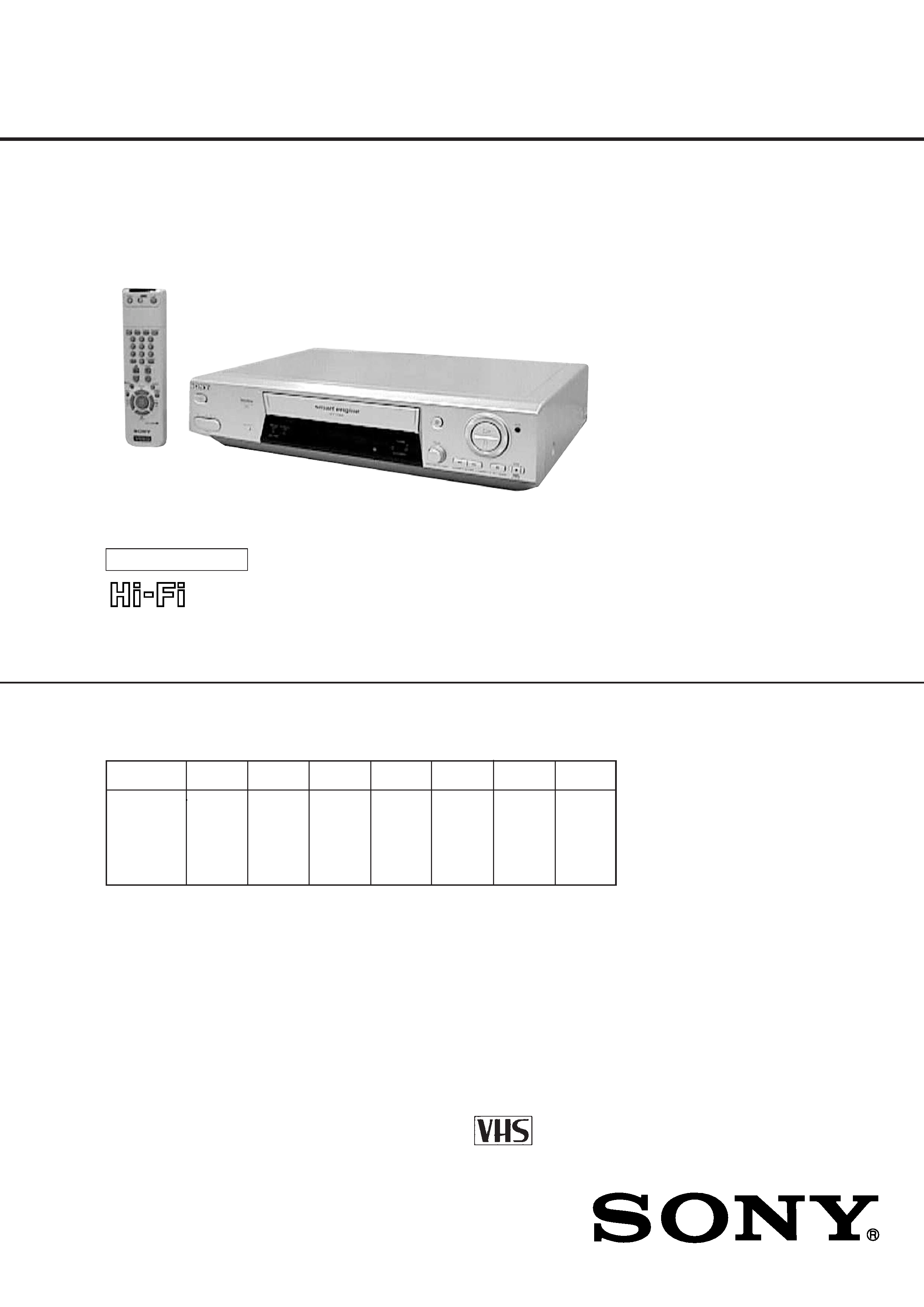
VIDEO CASSETTE RECORDER
· Refer to the SERVICE MANUAL of VHS MECHANICAL
ADJUSTMENTS VI for MECHANICAL ADJUSTMENTS.
(9-921-647-11)
* The abbreviations of SE610, SE710, SE810, SX710, SX717, SX810 and
X9 contained in this service manual are indicated when these models are
common to all their corresponding models as given below.
RMT-V259/V259B/V259K/V259L/V259R/V259S/V288/V288A/V288B/V288C
SLV-SE610/SE710/SE810/SX710/SX717/SX810/X9
Photo: SLV-SE810
SR MECHANISM
Abbreviated
SE610
SE710
SE810
SX710
SX717
SX810
X9
model name
SE610A
SE710B
SE810B
SX710B
SX717D
SX810D
X9B
All model
SE610B
SE710D
SE810D
SX710D
SX717E
X9D
names
SE610E
SE710E
SE810E
SX710E
X9E
SE610G
SE710G
SE810G
SX710K
X9G
SLV-
SE610K
SE710I
SE810K
SX710N
X9N
SE610N
SE710K
SE810N
SE710N

2
SAFETY CHECK-OUT
1. Check the area of your repair for unsoldered or poorly-sol-
dered connections. Check the entire board surface for solder
splashes and bridges.
2. Check the interboard wiring to ensure that no wires are
"pinched" or contact high-wattage resistors.
3. Look for unauthorized replacement parts, particularly transis-
tors, that were installed during a previous repair. Point them
out to the customer and recommend their replacement.
After correcting the original service problem, perform the following
safety checks before releasing the set to the customer:
4. Look for parts which, though functioning, show obvious signs
of deterioration. Point them out to the customer and recom-
mend their replacement.
5. Check the B+ voltage to see it is at the values specified.
SAFETY-RELATED COMPONENT WARNING!!
COMPONENTS IDENTIFIED BY MARK 0 OR DOTTED
LINE WITH MARK 0 ON THE SCHEMATIC DIAGRAMS
AND IN THE PARTS LIST ARE CRITICAL TO SAFE
OPERATION. REPLACE THESE COMPONENTS WITH
SONY PARTS WHOSE PART NUMBERS APPEAR AS
SHOWN IN THIS MANUAL OR IN SUPPLEMENTS PUB-
LISHED BY SONY.
SPECIFICATIONS
System
Channel coverage
SLV-SE610N/K, SE710N/K, SE810N/K, SX710N/K, X9N
PAL (B/G, D/K)
VHF E2E12, R1R12
UHF E21E69, R21R69
CATV S1S41, S01S05
SLV-SE610B, SE710B, SE810B, SX710B, X9B
SECAM (L):
VHF F2 to F10
UHF F21 to F69
CATV B to Q
HYPER S21 to S41
PAL (B/G):
VHF E2 to E12
VHF Italian channel A to H
UHF E21 to E69
CATV S01 to S05, S1 to S20
HYPER S21 to S41
RF output signal
SLV-SE610A/E, SE710D/E, SE810D/E, X9D/E,
SX710D/E, SX717D/E, SX810D/E
PAL (B/ G)
VHF E2 to E12
VHF Italian channel A to H
UHF E21 to E69
CATV S01 to S05,S1toS20
HYPER S21 to S41
SLVSE610G, SE710G/I, SE810G, X9G
PAL (I)
VHF IA to IJ, SA10 to SA13 (SLV-SE710I)
UHF B21 to B69
CATV S01 to S05, S1 to S20 (SLV-SE710I)
HYPER S21 to S41 (SLV-SE710I)
RF output signal
UHF channels 2169
Aerial out
75-ohm asymmetrical aerial socket
Tape speed
SLV-SE610N/K, SE710N/K, SE810N/K, SX710N/K, X9N
SP: PAL/MESECAM
23.39 mm/s (recording/playback)
NTSC
33.35 mm/s (playback only)
LP: PAL/MESECAM
11.70 mm/s (recording/playback)
NTSC
16.67 mm/s (playback only)
EP: NTSC
11.12 mm/s (playback only)
SLV-SE610B, SE710B, SE810B, SX710B, X9B
SP: PAL 23.39 mm/s (recording/playback)
NTSC 33.35 mm/s (playbackonly)
SECAM 23.39 mm/s (recording/playback)
MESECAM 23.39 mm/s (playback only)
LP: PAL 11.70 mm/s (recording/playback)
NTSC 16.67 mm/s (playback only)
SECAM 11.70 mm/s (recording/playback)
MESECAM 1.70 mm/s (playback only)
EP: NTSC 11.12 mm/s (playback only)
SLV-SE610A/E/G, SE710D/E/G/I, SE810D/E/G, X9D/E/G,
SX710D/E, SX717D/G, SX810D,
SP: PAL23.39 mm/s (recording/playback)
NTSC33.35 mm/s (playback only)
LP: PAL11.70 mm/s (recording/playback)
NTSC16.67 mm/s (playback only)
EP: NTSC11.12 mm/s (playback only)
Maximum recording/playback time
10 hrs. in LP mode (with E300 tape)
Fast-forward and rewind time
Approx. 1 min. (with E180 tape)

3
Inputs and outputs
i LINE-1 (TV)
21-pin
Video input: pin 20
Audio input: pins 2 and 6
Video output: pin 19
Audio output: pins 1 and 3
SLV-SE610E, SE710D/E/N/K, SX710D/E/N/K, SX717D/E
DECODER/t LINE-2 IN
21-pin
Video input: pin 20
Audio input: pins 2 and 6
SLV-SE810D/E/N/K, SX810D, X9E/N
DECODER/t LINE-3 IN
21-pin
Video input: pin 20
Audio input: pins 2 and 6
SLV-SE810D/E/N/K, SX810D, X9E/N
t LINE-2 L o R
VIDEO IN, phono jack (1)
Input signal: 1 Vp-p, 75 ohms,
unbalanced, sync negative
AUDIO IN, phono jack (2)
Input level: 327 mVrms
Input impedance: more than 47 kilohms
SLV-SE610B, SE710B, SX710B
DECODEUR/t ENTREE LIGNE-2
21-pin
Video input: pin 20
Audio input: pins 2 and 6
SLV-SE810B, X9B
DECODEUR/t ENTREE LIGNE-3
21-pin
Video input: pin 20
Audio input: pins 2 and 6
SLV-SE810B, X9B
t LIGNE-2 G o D
ENTREE VIDEO, phono jack (1)
Input signal: 1 Vp-p, 75 ohms,
unbalanced, sync negative
ENTREE AUDIO, phono jack (2)
Input level: 327 mVrms
Input impedance: more than 47 kilohms
SLV-SE710G, SE710I
t LINE-2 IN
21-pin
Video input: pin 20
Audio input: pins 2 and 6
SLV-SE810G,X9G
t LINE-3 IN
21-pin
Video input: pin 20
Audio input: pins 2 and 6
SLV-SE810G, X9G
t LINE-2 IN L o R
VIDEO IN, phono jack (1)
Input signal: 1 Vp-p, 75 ohms,
unbalanced, sync negative
AUDIO IN, phono jack (2)
Input level: 327 mVrms
Input impedance: more than 47 kilohms
o R/D L/G
Phono jack (2)
Rated output level: 327 mVrms
Load impedance: 47 kilohms
Output impedance: less than 10 kilohms
General
Power requirements
220 240 V AC, 50 Hz
Power consumption
20 W
SLV-610A/E, SE710D/E/N/K, SE810D/E/N/K, X9D/E/N,
SX710D/E/N/K, SX717D/E, SX810D
1.2 W (POWER SAVE is set to FULL/ON, minimum)
SLV-SE610G, SE710G/I, SE810G
1.2 W (POWER SAVE is set to ON, minimum)
SLV-SE610B, SE710B, SE810B, SX710B, X9B
1.2 W (VEILLE ECO is set to TOTAL, minimum)
Operating temperature
5°C to 40°C
Storage temperature
20°C to 60°C
Dimensions including projecting parts and controls
SLV-610A/E/B/N/K/G, SE710B/D/E/N/K/G/I,
SX710B/D/E/N/K, SX710D/E
Approx. 430
× 98 × 283 mm (w/h/d)
SLV-SE810B/D/E/N/K/G, SX810D
Approx. 430
× 98 × 289 mm (w/h/d)
SLV-X9
Approx. 430
× 110 × 285 mm (w/h/d)
Mass
EXCEPT SLV-X9
Approx. 4.1 kg
SLV-X9
Approx. 4.3 kg
Supplied accessories
Remote commander (1)
R6 (size AA) batteries (2)
Aerial cable (1)
Design and specifications are subject to change without notice.
4
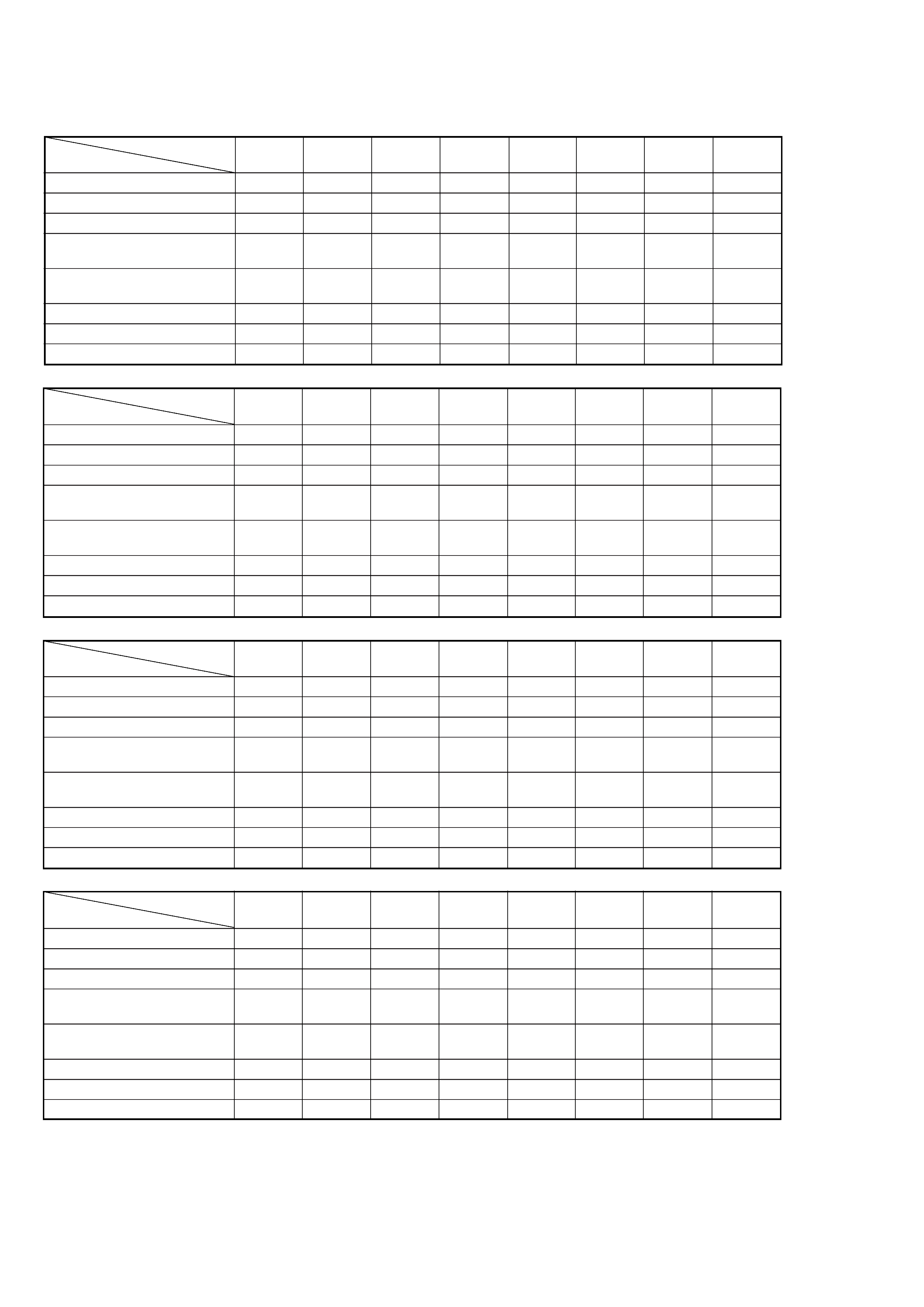
SLV-
SE610A
SE610B
SE610E
SE610G
SE610K
SE610N
SE710B
SE710D
FEATURE
SECAM (REC/PB)
×/×
a/a
×/××/××/××/×
a/a
×/×
ME-SECAM (REC/PB)
×/××/a
×/××/×
a/aa/a
×/a
×/×
EURO INPUT
21pin
21pin
× 2
21pin
× 2
21pin
21pin
21pin
21pin
× 2 21pin × 2
RCA FRONT LINE INPUT
×
×
××
×
×
××
ADDITIONAL REAR OUTPUT
××
×
×
×
×
2pin
2pin
(AUDIO OUT)
(R.W)
(R.W)
MODULATOR SYSTEM
G
L/G
G
I
G/K
G/K
L/G
G
STB CONTROL
×
×
××
×
×
××
REMOTE COMMANDER RMT-
V288B
V288C
V288B
V288B
V288B
V288B
V288C
V228B
SLV-
SE710E
SE710G
SE710I
SE710K
SE710N
SE810B
SE810D
SE810E
FEATURE
SECAM (REC/PB)
×/××/××/××/××/×
a/a
×/××/×
ME-SECAM (REC/PB)
×/××/××/×
a/aa/a
×/a
×/××/×
EURO INPUT
21pin
× 2 21pin × 2
21pin
× 2 21pin × 2
21pin
× 2 21pin × 2
21pin
× 2 21pin × 2
RCA FRONT LINE INPUT
××
×
×
×
3pin
3pin
3pin
(R.W.Y)
(R.W.Y)
(R.W.Y)
ADDITIONAL REAR OUTPUT
2pin
2pin
2pin
2pin
2pin
2pin
2pin
2pin
(AUDIO OUT)
(R.W)
(R.W)
(R.W)
(R.W)
(R.W)
(R.W)
(R.W)
(R.W)
MODULATOR SYSTEM
G
I
I
G/K
G/K
L/G
G
G
STB CONTROL
×
×
××
×
×
××
REMOTE COMMANDER RMT-
V288B
V288B
V288B
V288B
V288B
V259L
V259K
V259K
SLV-
SE810G
SE810K
SE810N
SX710B
SX710D
SX710E
SX710K
SX710N
FEATURE
SECAM (REC/PB)
×/××/××/×
a/a
×/××/××/××/×
ME-SECAM (REC/PB)
×/×
a/aa/a
×/a
×/××/×
a/aa/a
EURO INPUT
21pin
× 2 21pin × 2
21pin
× 2 21pin × 2
21pin
× 2 21pin × 2
21pin
× 2 21pin × 2
RCA FRONT LINE INPUT
3pin
3pin
3pin
××
×
×
×
(R.W.Y)
(R.W.Y)
(R.W.Y)
ADDITIONAL REAR OUTPUT
2pin
2pin
2pin
2pin
2pin
2pin
2pin
2pin
(AUDIO OUT)
(R.W)
(R.W)
(R.W)
(R.W)
(R.W)
(R.W)
(R.W)
(R.W)
MODULATOR SYSTEM
I
G/K
G/K
L/G
G
G
G/K
G/K
STB CONTROL
×
×
××
×
×
××
REMOTE COMMANDER RMT-
V259K
V259K
V259K
V288A
V288
V288
V288
V288
SLV-
SX717D
SX717E
SX810D
X9B
X9D
X9E
X9G
X9N
FEATURE
SECAM (REC/PB)
×/××/××/×
a/a
×/××/××/××/×
ME-SECAM (REC/PB)
×/××/××/××/a
×/××/××/×
a/a
EURO INPUT
21pin
× 2 21pin × 2
21pin
× 2 21pin × 2
21pin
× 2 21pin × 2
21pin
× 2 21pin × 2
RCA FRONT LINE INPUT
××
3pin
3pin
3pin
3pin
3pin
3pin
(R.W.Y)
(R.W.Y)
(R.W.Y)
(R.W.Y)
(R.W.Y)
(R.W.Y)
ADDITIONAL REAR OUTPUT
2pin
2pin
2pin
2pin
2pin
2pin
2pin
2pin
(AUDIO OUT)
(R.W)
(R.W)
(R.W)
(R.W)
(R.W)
(R.W)
(R.W)
(R.W)
MODULATOR SYSTEM
G
G
G
L/G
G
G
I
G/K
STB CONTROL
××
×
a
aaa
×
REMOTE COMMANDER RMT-
V259
V259
V259
V259S
V259R
V259R
V259R
V259B
· Feature Difference

5
TABLE OF CONTENTS
Section
Title
Page
Section
Title
Page
Feature Difference ................................................................... 4
SERVICE NOTE ...................................................................... 6
1.
GENERAL
Getting Started .............................................................. 1-1
Basic Operations ........................................................... 1-11
Additional Operations .................................................... 1-15
Editing ............................................................................ 1-21
2.
DISASSEMBLY
2-1.
Upper Case Removal .................................................... 2-1
2-2.
Rear Panel Removal ..................................................... 2-1
2-3.
Power Block (SRV938EK) Removal .............................. 2-1
2-4.
Front Panel Section Removal ........................................ 2-1
2-5.
Mechanism Deck Removal ............................................ 2-2
2-6.
MA-400 Board Removal ................................................ 2-2
2-7.
Internal Views ................................................................ 2-3
2-8.
Circuit Boards Location ................................................. 2-4
3.
BLOCK DIAGRAMS
3-1.
Overall Block Diagram ................................................... 3-1
3-2.
Video Block Diagram ..................................................... 3-3
3-3.
Servo/System Control Block Diagram .......................... 3-5
3-4.
Audio Block Diagram ..................................................... 3-7
3-5.
Tuner Block Diagram ..................................................... 3-9
3-6.
Mode Control Block Diagram ........................................ 3-11
3-7.
Power Block Diagram .................................................... 3-13
4.
PRINTED WIRING BOARDS AND
SCHEMATIC DIAGRAMS
4-1.
Frame Schematic Diagram ............................................ 4-3
4-2.
Printed Wiring Boards and Schematic Diagrams ......... 4-5
MA-400 Printed Wiring Board ....................................... 4-5
MA-400 (Video, Audio) Schematic Diagram ................. 4-9
MA-400 (SECAM) Schematic Diagram ......................... 4-11
MA-400 (Servo/System Control)
Schematic Diagram ....................................................... 4-13
MA-400 (Hi-Fi Audio) Schematic Diagram .................... 4-17
MA-400 (I/O) Schematic Diagram ................................. 4-19
MA-400 (Tuner) Schematic Diagram ............................ 4-21
MA-400 (Mode Control) Schematic Diagram ................ 4-23
MA-400 (Power Supply) Schematic Diagram ............... 4-25
DS-95 Schematic Diagram ............................................ 4-27
JK-201 Schematic Diagram .......................................... 4-27
DS-95 Printed Wiring Board .......................................... 4-29
JK-201 Printed Wiring Board ........................................ 4-29
SRV938EK Printed Wiring Board .................................. 4-31
SRV938EK Schematic Diagram .................................... 4-33
5.
INTERFACE, IC PIN FUNCTION DESCRIPTION
5-1.
System Control-Video Block Interface
(MA-400 BOARD IC162) ............................................... 5-1
5-2.
System Control-Servo Peripheral Circuit Interface
(MA-400 BOARD IC162) ............................................... 5-1
5-3.
System Control-Mechanism Block Interface
(MA-400 BOARD IC162) ............................................... 5-2
5-4.
System Control-System Control Peripheral Circuit
Interface (MA-400 BOARD IC162) ................................ 5-3
5-5.
System Control-Audio Block Interface
(MA-400 BOARD IC162) ............................................... 5-3
5-6.
Servo/System Control Microprocessor Pin Function
(MA-400 BOARD IC162) ............................................... 5-4
5-7.
Mode Control Pin Function
(MA-400 BOARD IC420) ............................................... 5-5
6.
ERROR CODES ....................................................... 6-1
7.
ADJUSTMENTS
7-1.
Mechanical Adjustments ............................................... 7-1
7-2.
Electrical Adjustments ................................................... 7-1
2-1.
Pre-Adjustment Preparations ........................................ 7-1
2-1-1. Instruments to be Used ............................................ 7-1
2-1-2. Connection ............................................................... 7-1
2-1-3. Set-up of Adjustment ............................................... 7-1
2-1-4. Alignment Tapes ....................................................... 7-1
2-1-5. Specified I/O Level and Impedance ......................... 7-1
2-1-6. Adjusting Sequence ................................................. 7-2
2-2.
Power Supply Adjustments ........................................... 7-2
2-2-1. Power Supply Check ................................................ 7-2
2-2-2. +6 V Adjustment ....................................................... 7-2
2-3.
Servo System Adjustment ............................................. 7-2
2-3-1. RF Switching Position Adjustment ........................... 7-2
2-4.
Audio System Adjustments ........................................... 7-3
2-4-1. Hi-Fi Audio System Adjustment ............................... 7-3
1.
AF Switching Position Adjustment ........................... 7-3
2.
Frequency Response Check .................................... 7-3
3.
Overall Level Characteristic and
Distortion Factor Check ........................................... 7-4
4.
Overall S/N Check .................................................... 7-4
2-4-2. Normal Audio System Adjustment ........................... 7-4
1.
ACE Head Adjustment ............................................. 7-4
2.
E-E Output Level Check ........................................... 7-4
3.
Frequency Response Check .................................... 7-4
4.
Overall Level Characteristic and Distortion
Factor Check ............................................................ 7-5
5.
Overall S/N Check .................................................... 7-5
2-5.
Parts Arrangement Diagram for Adjustments ............... 7-6
8.
REPAIR PARTS LIST
8-1.
Exploded Views ............................................................. 8-1
8-1-1. Front Panel and Cabinet Assemblies ....................... 8-1
8-1-2. Chassis Assembly .................................................... 8-3
8-1-3. Mechanism Chassis Assembly (1) ........................... 8-4
8-1-4. Mechanism Chassis Assembly (2) ........................... 8-5
8-1-5. Mechanism Chassis Assembly (3) ........................... 8-6
8-2.
Electrical Parts List ....................................................... 8-7