MICROFILM
SERVICE MANUAL
Australian Model
SLV-EZ8AS/EZ9AS
E Model
SLV-ED8ML
ME Model
SLV-ED8ME
NewZealand Model
SLV-EZ8NZ
RMT-V243/V245
VIDEO CASSETTE RECORDER
SLV-ED8ME/ED8ML/EZ8AS/
EZ8NZ/EZ9AS
G
· Refer to the SERVICE MANUAL of VHS MECHANICAL
ADJUSTMENTS VI for MECHANICAL ADJUSTMENTS.
(9-921-647-11)
* The abbreviations of ED8, EZ8 and EZ9 contained in this service manual are
indicated when these models are common to all their corresponding models
as given below.
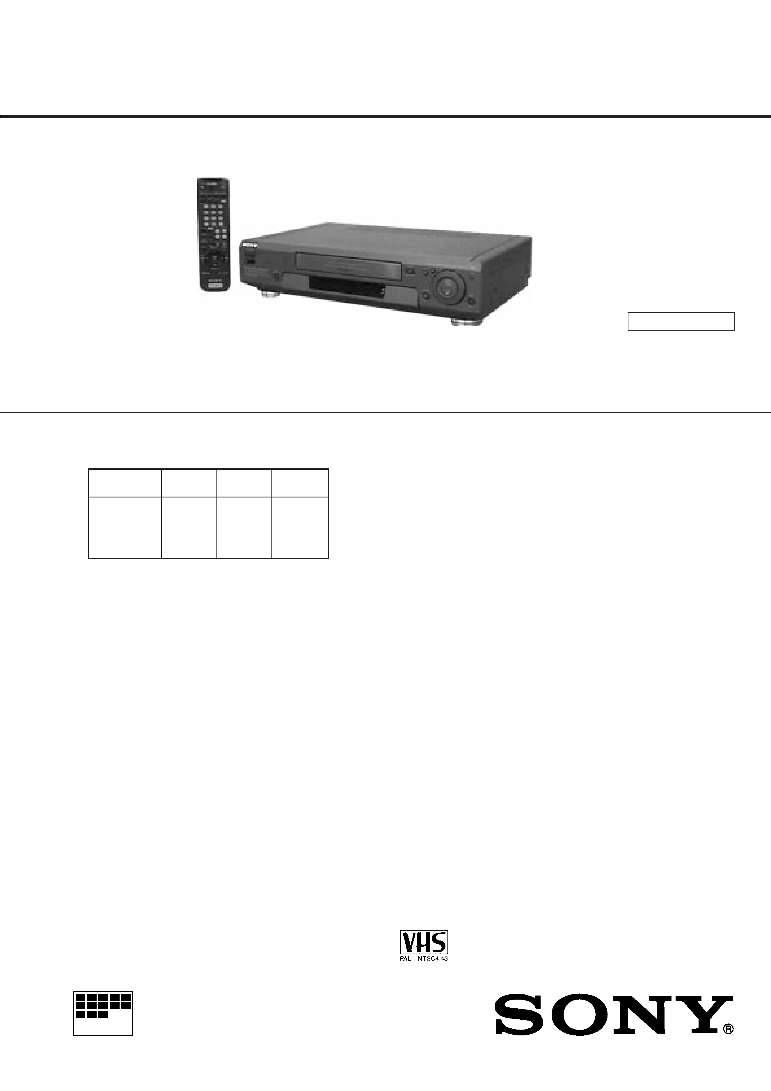
Photo: SLV-ED8ML
S MECHANISM
ED8ME
ED8ML
ED8
Abbreviated
model name
All model
names
SLV-
EZ8AS
EZ8NZ
EZ8
EZ9AS
EZ9
System
Color system
ED8:
PAL, MESECAM, NTSC 3.58,
NTSC 4.43
EZ8/EZ9:
PAL, NTSC 4.43
TV system
ED8:
B/G, D/K, I
EZ8/EZ9
B/G
Channel coverage
ED8:
B/G: VHF E2 to E12/UHF E21 to E69/
CATV S01 to S05, S1 to S41
D/K: VHF R1 to R12, UHF R21 to R69
I: VHF SA4 to SA13/UHF B21 to B69/
CATV S01 to S05, S1 to S41
M: VHF A2 to A13/UHF A14 to A69/
CATV A-8 to A1, A to W, W+1 to W+84
EZ8AS/EZ9AS:
VHF AS0 to AS12, AS5A, AS9A
UHF AS28 to AS69
CATV S01 to S05, S1 to S41
SPECIFICATIONS
EZ8NZ:
VHF NZ1 to NZ11
UHF E21 to E69
CATV S01 to S05, S1 to S41
Stereo system
ED8/EZ8NZ:
NICAM STEREO: B/G, I
ZWEITON German stereo: B/G
ED8AS/EZ9AS:
ZWEITON German stereo: B/G
RF output signal
ED8/EZ8NZ:
UHF channels 21 to 69
EZ8AS/EZ9AS:
UHF channels 28 to 69
Aerial out
75-ohm asymmetrical aerial socket
Inputs and outputs
LINE-1, 2-IN
VIDEO IN, phono jack (1)
Input signal: 1 Vp-p, 75 ohms, unbalanced,
sync negative
AUDIO IN, phono jack (2)
Input level: 327 mVrms
Input impedance: more than 47 kilohms
LINE-3 IN (SAT IN) (ED8, EZ9)
VIDEO IN, phono jack (1)
Input signal: 1Vp-p, 75 ohms, unbalanced,
sync negative
AUDIO IN, phono jack (2)
Input level: 327mVrms
Input impedance: more than 47 kilohms
Continued on next page
2
SAFETY CHECK-OUT
1. Check the area of your repair for unsoldered or poorly-sol-
dered connections. Check the entire board surface for solder
splashes and bridges.
2. Check the interboard wiring to ensure that no wires are
"pinched" or contact high-wattage resistors.
3. Look for unauthorized replacement parts, particularly transis-
tors, that were installed during a previous repair. Point them
out to the customer and recommend their replacement.
After correcting the original service problem, perform the following
safety checks before releasing the set to the customer:
4. Look for parts which, though functioning, show obvious signs
of deterioration. Point them out to the customer and recom-
mend their replacement.
5. Check the B+ voltage to see it is at the values specified.
SAFETY-RELATED COMPONENT WARNING!!
COMPONENTS IDENTIFIED BY MARK
! OR DOTTED
LINE WITH MARK
! ON THE SCHEMATIC DIAGRAMS
AND IN THE PARTS LIST ARE CRITICAL TO SAFE
OPERATION. REPLACE THESE COMPONENTS WITH
SONY PARTS WHOSE PART NUMBERS APPEAR AS
SHOWN IN THIS MANUAL OR IN SUPPLEMENTS PUB-
LISHED BY SONY.
LINE 1 OUT
VIDEO OUT, phono jack (1)
Output signal: 1 Vp-p, 75 ohms, unbal-
anced, sync negative
AUDIO OUT, phono jack (2)
Standard output: 327 mVrms
Load impedance; 47 kilohms
Output impedance: less than 10 kilohms
LINE 2 OUT (AUDIO)
AUDIO OUT, phono jack (2)
Standard output: 327 mVrms
Load impedance; 47 kilohms
Output impedance: less than 10 kilohms
SKY TV DECODER (EZ8NZ)
VIDEO IN, phono jack (1)
Input signal: 1 Vp-p, 75 ohms, unbalanced,
sync negative
VIDEO OUT, phono jack (1)
Output signal: 1 Vp-p, 75 ohms,
unbalanced, sync negative
General
Power requirements
110 240 V AC, 50/60 Hz (ED8)
220-240 V AC, 50 Hz (EZ8/EZ9)
Power consumption
22W (ED8)
23W (EZ8/EZ9)
Operating temperature
5 °C to 40 °C
Storage temperature
20 °C to 60 °C
Dimensions
Approx. 430
× 100 × 286 mm (w/h/d):
including projecting parts and controls
Mass
Approx. 5.7 kg: (ED8)
Approx. 5.9 kg: (EZ8/EZ9)
Supplied accessories
Remote commander (1)
R6 (size AA) batteries (2)
Aerial cable (1)
Plug adaptor (1) (ED8)
Audio/Video cable (3-phono to 3-phono) (1)
Design and specifications are subject to change
without notice.
SLV-
ED8
EZ8
EZ8
EZ9
FEATURE
AS
NZ
AS
ME-SECAM
(REC/PB)
®/®G/GG/GG/G
ADDITIONAL REAR INPUT (SAT IN)
®G
G®
SKY TV DECODER IN/OUT
G/GG/G®/®G/G
MODULATOR SYSTEM
G,K,I,M
G
G
G
CLICK/JOG SHUTTLE (REMOTE COMMANDER)
G/GG/GG/G®/®
REMOTE COMMANDER
RMT-
V245
V245
V245
V243
· Feature Difference

3
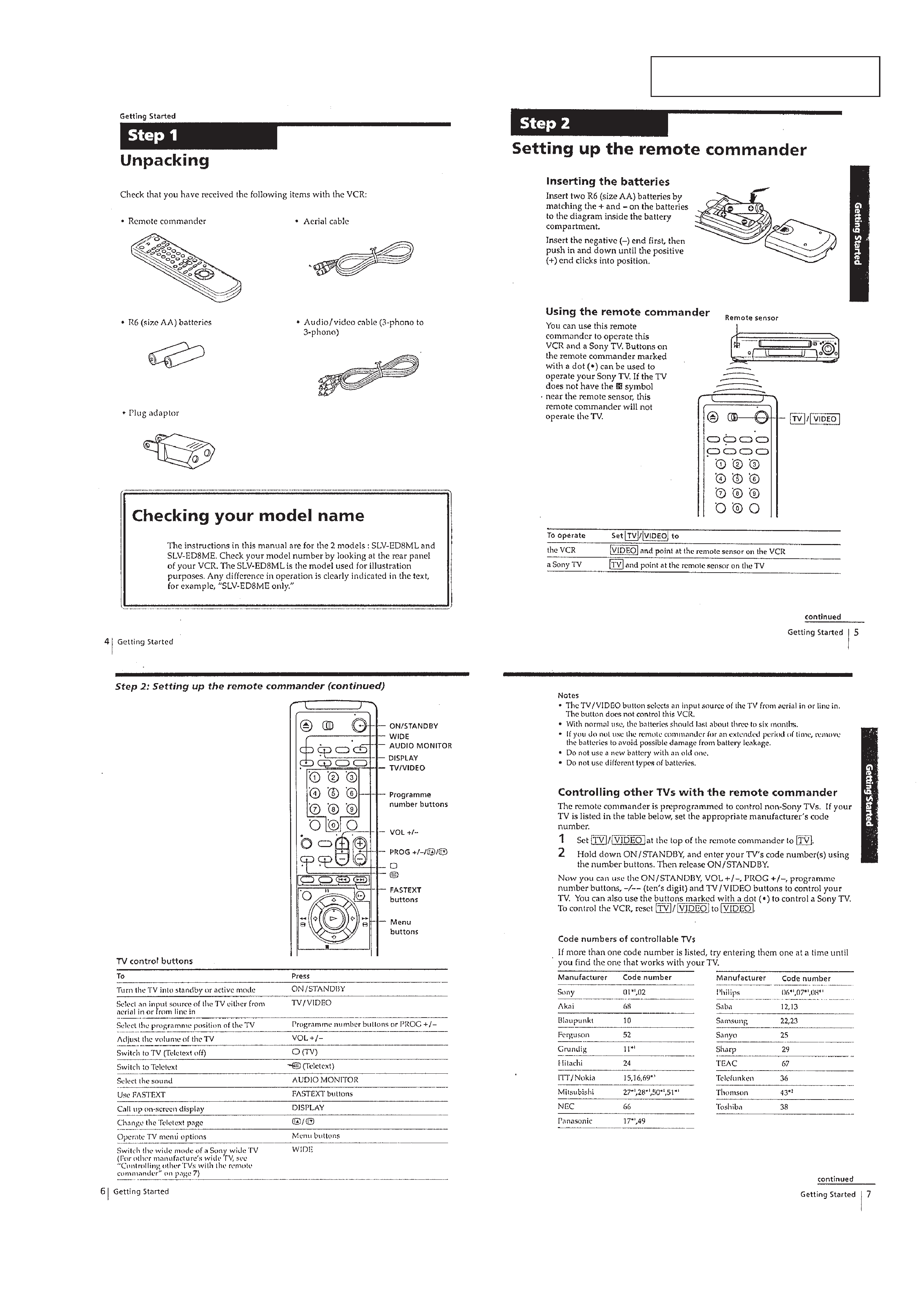
TABLE OF CONTENTS
Section
Title
Page
Section
Title
Page
Feature Difference ................................................................... 2
SERVICE NOTE ...................................................................... 4
1.
GENERAL
Getting Started .............................................................. 1-1
Basic Operations ........................................................... 1-9
Additional Operations .................................................... 1-13
Editing ............................................................................ 1-15
Additional Information ................................................... 1-16
2.
DISASSEMBLY
2-1.
Upper Case Removal .................................................... 2-1
2-2.
RJ-79, NK-11 Board Removal ....................................... 2-1
2-3.
Rear Panel Removal ..................................................... 2-1
2-4.
Front Panel Section Removal ....................................... 2-1
2-5.
FR-137, DM-77, SW-307, IO-64 Board
Removal (EZ9) .............................................................. 2-2
2-6.
Control Switch Block Removal (EZ9) ........................... 2-2
2-7.
FR-137, DM-77, IO-64 Board Removal (ED8/EZ8) ...... 2-2
2-8.
Mechanism Deck Removal ........................................... 2-2
2-9.
Power Block Removal ................................................... 2-3
2-10. PS-414, MA-325 board Removal .................................. 2-3
2-11. Internal Views ................................................................ 2-4
2-12. Circuit Boards Location ................................................. 2-5
3.
BLOCK DIAGRAMS
3-1.
Overall Block Diagram .................................................. 3-1
3-2.
Video1 Block Diagram ................................................... 3-4
3-3.
Video2 Block Diagram ................................................... 3-5
3-4.
Servo/System control Block Diagram ........................... 3-7
3-5.
Audio Block Diagram ..................................................... 3-9
3-6.
Tuner Block Diagram ..................................................... 3-11
3-7.
Mode Control Block Diagram ........................................ 3-13
3-8.
Power Block Diagram .................................................... 3-15
4.
PRINTED WIRING BOARDS AND
SCHEMATIC DIAGRAMS
4-1.
Frame Schematic Diagram ........................................... 4-3
4-2.
Printed Wiring Boards and Schematic Diagrams ......... 4-5
MA-325 (Head Amp) Schematic Diagram .................... 4-5
MA-325 Printed Wiring Board ....................................... 4-9
MA-325 (Video, Audio) Schematic Diagram ................. 4-11
MA-325 (System Control) Schematic Diagram ............ 4-15
MA-325 (Servo Control) Schematic Diagram ............... 4-17
MA-325 (Bias, CTL) Schematic Diagram ..................... 4-19
MA-325 (Hi-Fi Audio) Schematic Diagram .................... 4-21
MA-325 (OSD) Schematic Diagram .............................. 4-23
MA-325 (IO) Schematic Diagram .................................. 4-25
MA-325 (Tuner) Schematic Diagram ............................ 4-27
IO-64 Printed Wiring Board and
Schematic Diagram ....................................................... 4-30
RJ-79 Printed Wiring Board and Schematic Diagram .. 4-31
NK-11 Printed Wiring Board and
Schematic Diagram ....................................................... 4-33
DM-77 Printed Wiring Board and
Schematic Diagram ....................................................... 4-35
FR-137, SW-307 Printed Wiring Boards ....................... 4-37
FR-137, SW-307 Schematic Diagram .......................... 4-39
PS-414 Printed Wiring Board ........................................ 4-41
PS-414 Schematic Diagram .......................................... 4-43
SR-718 Printed Wiring Board ....................................... 4-45
SR-718 Schematic Diagram ......................................... 4-47
5.
INTERFACE, IC PIN FUNCTION DESCRIPTION
5-1.
System Control-Video Block Interface
(MA-325 board IC161) .................................................. 5-1
5-2.
System Control-Servo Peripheral Circuit Interface
(MA-325 board IC161) .................................................. 5-1
5-3.
System Control-Mechanism Interface
(MA-325 board IC161) .................................................. 5-2
5-4.
System Control-System Control Peripheral Circuit
Interface (MA-325 board IC161) ................................... 5-3
5-5.
System Control-Hi-Fi Audio Block Interface
(MA-325 board IC161) .................................................. 5-3
5-6.
Servo/System Control Microprocessor Pin Function
(MA-325 board IC161) .................................................. 5-4
5-7.
Timer/Tuner Control Microprocessor Pin Function
(FR-137 board IC301) ................................................... 5-5
5-8.
Nicam Processor Pin Function
(NK-11 board IC1) ......................................................... 5-6
6.
ERROR CODE .......................................................... 6-1
7.
ADJUSTMENTS
7-1.
Mechanical Adjustments ............................................... 7-1
7-2.
Electrical Adjustments ................................................... 7-1
2-1.
Pre-Adjustment Preparations ........................................ 7-1
2-1-1. Instruments to be Used ............................................ 7-1
2-1-2. Connection ............................................................... 7-1
2-1-3. Set-up of Adjustment ................................................ 7-1
2-1-4. Alignment Tape ......................................................... 7-1
2-1-5. Specified I/O Level and Impedance ......................... 7-1
2-1-6. Adjusting Sequence ................................................. 7-2
2-2.
Power Supply Adjustment ............................................. 7-2
2-2-1. Power Supply Check ................................................ 7-2
2-2-2. +6V Adjustment ........................................................ 7-2
2-3.
Servo System Adjustment ............................................. 7-2
2-3-1. RF Switching Position Adjustment ........................... 7-2
2-4.
Audio System Adjustments ........................................... 7-3
2-4-1. Hi-Fi Audio System Adjustment ............................... 7-3
1.
AF Switching Position Adjustment ........................... 7-3
2.
Frequency Response Check .................................... 7-3
3.
Overall Level Characteristic and
Distortion Factor Check ........................................... 7-4
4.
Overall S/N Check .................................................... 7-4
2-4-2. Normal Audio System Adjustment ........................... 7-4
1.
ACE Head Adjustment ............................................. 7-4
2.
E-E Output Level Check .......................................... 7-4
3.
Frequency Responce Check .................................... 7-4
4.
Overall Level Characteristic and Distortion
Factor Check ............................................................ 7-5
5.
Overall S/N Check .................................................... 7-5
2-5.
Video System Adjustment ............................................. 7-5
2-5-1. VCO Oscillation Frequency Adjustment .................. 7-5
2-6.
Parts Arrangement Diagram for Adjustments ............... 7-6
8.
REPAIR PARTS LIST
8-1.
Exploded Views ............................................................. 8-1
8-1-1. Front Panel and Cabinet Assemblies
(ED8/EZ8) ................................................................ 8-1
8-1-2. Front panel and Cabinet Assemblies
(EZ9) ......................................................................... 8-2
8-1-3. Chassis Assembly .................................................... 8-3
8-1-4. Mechanism Chassis Assembly (1) ........................... 8-4
8-1-5. Mechanism Chassis Assembly (2) ........................... 8-5
8-1-6. Mechanism Chassis Assembly (3) ........................... 8-6
8-2.
Electrical Parts List ........................................................ 8-7
4
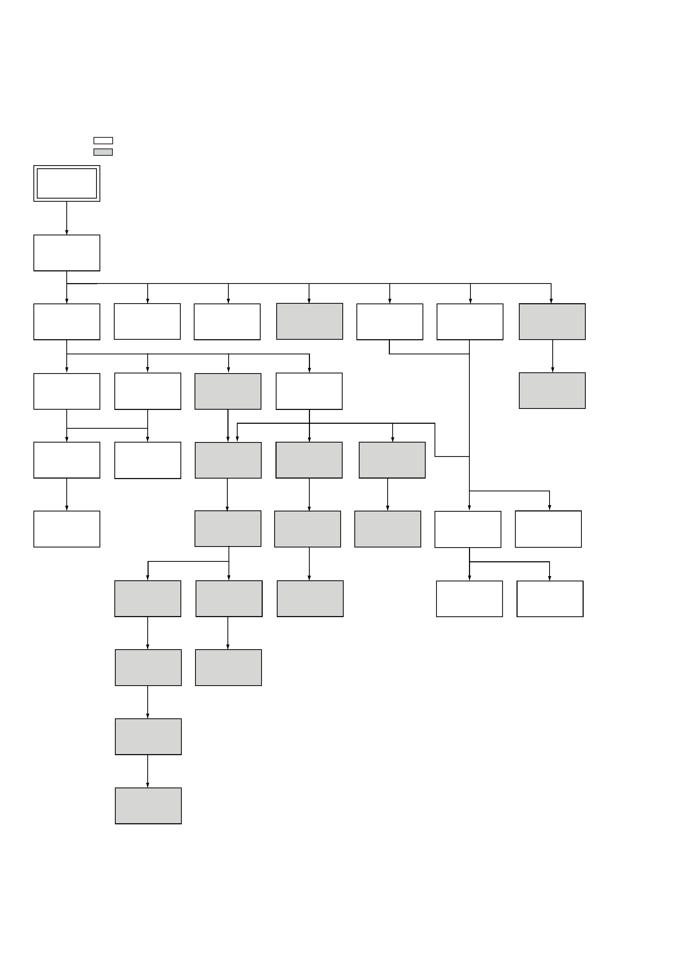
SERVICE NOTE
1. DISASSEMBLY
· This set can be disassembled in the order shown below.
Note: Pages in
indicated pages in the SERVICE MANUAL.
Pages in
indicated pages in the VHS MECHANICAL ADJUSTMENT MANUAL VI.
NK-11 Board
(ED8/EZ8NZ)
(Page 2-1)
Set
Upper case
(Page 2-1)
Front Panel
Section
(Page 2-1)
Power
Block
(Page 2-3)
Rear Panel
(Page 2-1)
Pinch Press
Block Ass'y
(Page 14)
Ground Shaft
Ass'y
(Page 13)
Drum Ass'y
(Page 13)
RJ-79 Board
(Page 2-1)
Mechanism
Deck
(Page 2-2)
FR-137 Board
(Page 2-2)
FL complete
Ass'y
(Page 13)
FL Slider
Block Ass'y
(Page 22)
DM-77 Board
(Page 2-2)
SW-307 Board
(EZ9)
(Page 2-2)
Rubber
Belt
(Page 15)
IO-64 Board
(Page 2-2)
Retainer
Plate
(Page 22)
Rubber
Belt
(Page 15)
Capstan
Motor
(Page 15)
Control Switch
Block (EZ9)
(Page 2-2)
Rotary
Switch
(Page 2-2)
Tuner
Unit
Pully Gear
Ass'y
(Page 29)
Cam Gear
(Page 23)
Cam Motor
Retainer
(Page 31)
Rubber
Belt
(Page 15)
Reel Direct
Ass'y
(Page 30)
Slider
(Page 26)
Loading
Gear (T, S)
(Page 28)
Cam Motor
(Page 31)
MA-325 Board
(Page 2-3)
PS-414 Board
(Page 2-3)
1-1
SECTION 1
GENERAL
This section is extracted from SLV-
ED8ME/ML instruction manual.
SLV-ED8/EZ8/EZ9