ORDER NO.
PIONEER CORPORATION 4-1, Meguro 1-chome, Meguro-ku, Tokyo 153-8654, Japan
PIONEER ELECTRONICS (USA) INC. P.O. Box 1760, Long Beach, CA 90801-1760, U.S.A.
PIONEER EUROPE NV Haven 1087, Keetberglaan 1, 9120 Melsele, Belgium
PIONEER ELECTRONICS ASIACENTRE PTE. LTD. 253 Alexandra Road, #04-01, Singapore 159936
PIONEER CORPORATION 2008
2008 Printed in Japan
MASTER
VOLUME
VSX-518
STANDBY/ON
PHONES
DVD
TV
DVD 5.1
DVR
CD
CD-R
FM
AM
MIDNIGHT/
LOUDNESS
VSB MODE
SIGNAL
SELECT
SOUND
RETRIEVER
PORTABLE
PORTABLE
SLEEP
PHASE
CONTROL
INPUT
SELECTOR
ADVANCED
SURROUND
STEREO /
A.L.C.
STANDARD
AUDIO/VIDEO MULTI-CHANNEL RECEIVER
DIALOGUE
ENHANCEMENT
PHASE
CONTROL
AUTO SURR /
STREAM DIRECT
VSX-518-K
RRV3707
AUDIO/VIDEO MULTI-CHANNEL RECEIVER
VSX-518-K
VSX-518-S
THIS MANUAL IS APPLICABLE TO THE FOLLOWING MODEL(S) AND TYPE(S).
Model
Type
Power Requirement
Remarks
VSX-518-K
KUCXJ
AC 120 V
VSX-518-S
KUCXJ
AC 120 V
For details, refer to "Important Check Points for good servicing".
T-ZZK JAN.
2
VSX-518-K
1
2
3
4
A
B
C
D
E
F
1
2
3
4
SAFETY INFORMATION
This service manual is intended for qualified service technicians; it is not meant for the casual
do-it-yourselfer. Qualified technicians have the necessary test equipment and tools, and have been
trained to properly and safely repair complex products such as those covered by this manual.
Improperly performed repairs can adversely affect the safety and reliability of the product and may
void the warranty. If you are not qualified to perform the repair of this product properly and safely, you
should not risk trying to do so and refer the repair to a qualified service technician.
WARNING
This product contains lead in solder and cer tain electrical par ts contain chemicals which are known to the state of California to
cause cancer, bir th defects or other reproductive harm.
Health & Safety Code Section 25249.6 Ð Proposition 65
NOTICE
(FOR CANADIAN MODEL ONLY)
Fuse symbols
(fast operating fuse)
and/or
(slow operating fuse) on PCB indicate that replacement
parts must be of identical designation.
REMARQUE
(POUR MODÈLE CANADIEN SEULEMENT)
Les symboles de fusible
(fusible de type rapide)
et/ou
(fusible de type lent) sur CCI indiquent que
les pièces de remplacement doivent avoir la même désignation.
ANY MEASUREMENTS NOT WITHIN THE
LIMITS OUTLINED ABOVE ARE INDICATIVE
OF A POTENTIAL SHOCK HAZARD AND
MUST BE CORRECTED BEFORE RETURN-
ING THE APPLIANCE TO THE CUSTOMER.
2. PRODUCT SAFETY NOTICE
Many electrical and mechanical parts in the appliance
have special safety related characteristics. These are
often not evident from visual inspection nor the
protection afforded by them necessarily can be obtained
by using replacement components rated for voltage,
wattage, etc. Replacement par ts which have these
special safety character istics are identified in this
Service Manual.
Electr ical components having such features are
identified by marking with a
on the schematics and
on the parts list in this Service Manual.
The use of a substitute replacement component which
does not have the same safety characteristics as the
PIONEER recommended replacement one, shown in the
parts list in this Service Manual, may create shock, fire,
or other hazards.
Product Safety is continuously under review and new
instructions are issued from time to time. For the latest
infor mation, always consult the current PIONEER
Service Manual. A subscription to, or
additional copies
of, PIONEER Ser vice Manual may be obtained at a
nominal charge from PIONEER.
(FOR USA MODEL ONLY)
1. SAFETY PRECAUTIONS
The following check should be perfor med for the
continued protection of the customer and ser vice
technician.
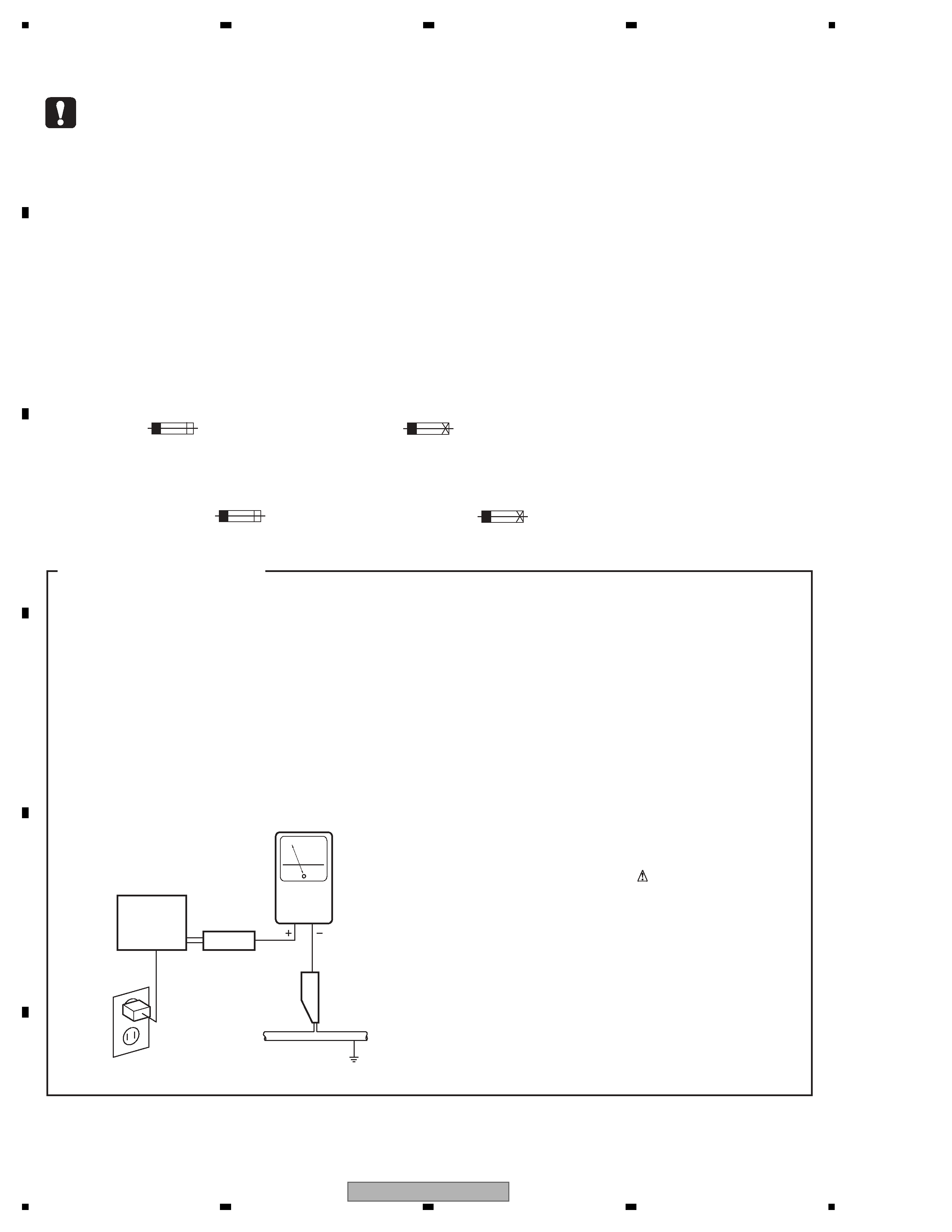
LEAKAGE CURRENT CHECK
Measure leakage current to a known ear th ground
(water pipe, conduit, etc.) by connecting a leakage
current tester such as Simpson Model 229-2 or
equivalent between the ear th ground and all exposed
metal par ts of the appliance (input/output ter minals,
screwheads, metal overlays, control shaft, etc.). Plug
the AC line cord of the appliance directly into a 120V
AC 60 Hz outlet and turn the AC power switch on. Any
current measured must not exceed 0.5 mA.
Device
under
test
Leakage
current
tester
Earth
ground
Reading should
not be above
0.5 mA
Also test with
plug reversed
(Using AC adapter
plug as required)
Test all
exposed metal
surfaces
AC Leakage Test
3
VSX-518-K
5
6
7
8
5
6
7
8
A
B
C
D
E
F

4
VSX-518-K
1
2
3
4
A
B
C
D
E
F
1
2
3
4
CONTENTS
SAFETY INFORMATION ..........................................................................................................................................................2
1. SERVICE PRECAUTIONS ....................................................................................................................................................5
1.1 NOTES ON SOLDERING ...............................................................................................................................................5
1.2 AMPLIFIER FAILURE DIAGNOSIS FLOW CHART........................................................................................................5
2. SPECIFICATIONS .................................................................................................................................................................6
2.1 SPECIFICATIONS...........................................................................................................................................................6
2.2 PANEL FACILITIES .........................................................................................................................................................7
3. BASIC ITEMS FOR SERVICE.............................................................................................................................................12
3.1 CHECK POINTS AFTER SERVICING..........................................................................................................................12
3.2 PCB LOCATIONS .........................................................................................................................................................13
4. BLOCK BIAGRAM ...............................................................................................................................................................14
4.1 OVERALL WIRING CONNECTION DIAGRAM ............................................................................................................14
4.2 BLOCK DIAGRAM ........................................................................................................................................................16
4.3 DSP BLOCK DIAGRAM................................................................................................................................................18
5. DIAGNOSIS.........................................................................................................................................................................19
5.1 DIAGNOSIS FLOWCHART (DSP ASSY) .....................................................................................................................19
5.2 DETECTION CIRCUIT..................................................................................................................................................23
5.3 AMPLIFIER SYSTEM PROTECTION OPERATION SPECIFICATION .........................................................................25
6. SERVICE MODE .................................................................................................................................................................26
7. DISASSEMBLY....................................................................................................................................................................27
8. EACH SETTING AND ADJUSTMENT ................................................................................................................................29
9. EXPLODED VIEWS AND PARTS LIST...............................................................................................................................30
9.1 PACKING ......................................................................................................................................................................30
9.2 EXTERIOR SECTION...................................................................................................................................................32
9.3 REAR PANEL SECTION...............................................................................................................................................34
9.4 FRONT PANEL SECTION ............................................................................................................................................36
10. SCHEMATIC DIAGRAM ....................................................................................................................................................38
10.1 MAIN ASSY (1/3) ........................................................................................................................................................38
10.2 MAIN ASSY (2/3) ........................................................................................................................................................40
10.3 MAIN ASSY (3/3) ........................................................................................................................................................42
10.4 DSP ASSY (1/2)..........................................................................................................................................................44
10.5 DSP ASSY (2/2)..........................................................................................................................................................46
10.6 POWER PACK (1/2) and TRANS2 ASSY ...................................................................................................................48
10.7 POWER PACK ASSY (2/2) .........................................................................................................................................50
10.8 COMPONENT VIDEO, 5.1CH INPUT and TRANS3 ASSYS .....................................................................................52
10.9 FRONT DISPLAY, ROTARY ENCODER, POWER KEY and JOG ASSYS .................................................................54
10.10 FRONT MINI JACK, DIGITAL INPUT, REGULATOR and HEAD PHONE ASSYS....................................................56
10.11 VIDEO, PRIMARY and TRANS1 ASSYS..................................................................................................................58
11. PCB CONNECTION DIAGRAM ........................................................................................................................................60
11.1 DSP ASSY ..................................................................................................................................................................61
11.2 MAIN ASSY ................................................................................................................................................................62
11.3 POWER PACK ASSY..................................................................................................................................................66
11.4 TRANS2 and TRANS3 ASSYS...................................................................................................................................70
11.5 COMPONENT VIDEO ASSY ......................................................................................................................................72
11.6 5.1CH INPUT and HEAD PHONE ASSYS .................................................................................................................73
11.7 FRONT DISPLAY, ROTARY ENCODER, POWER KEY and JOG ASSYS .................................................................74
11.8 DIGITAL INPUT ASSY ................................................................................................................................................78
11.9 REGULATOR ASSY....................................................................................................................................................79
11.10 VIDEO ASSY ............................................................................................................................................................80
11.11 FRONT MINI JACK ASSY.........................................................................................................................................81
11.12 TRANS1 and PRIMARY ASSYS...............................................................................................................................82
12. ELECTRICAL PARTS LIST ...............................................................................................................................................84

5
VSX-518-K
5
6
7
8
5
6
7
8
A
B
C
D
E
F
1. SERVICE PRECAUTIONS
1.1 NOTES ON SOLDERING
1.2 AMPLIFIER FAILURE DIAGNOSIS FLOW CHART
· For environmental protection, lead-free solder is used on the printed circuit boards mounted in this unit.
Be sure to use lead-free solder and a soldering iron that can meet specifications for use with lead-free solders for repairs
accompanied by reworking of soldering.
· Compared with conventional eutectic solders, lead-free solders have higher melting points, by approximately 40
°C.
Therefore, for lead-free soldering, the tip temperature of a soldering iron must be set to around 373
°C in general, although
the temperature depends on the heat capacity of the PC board on which reworking is required and the weight of the tip of
the soldering iron.
Do NOT use a soldering iron whose tip temperature cannot be controlled.
Compared with eutectic solders, lead-free solders have higher bond strengths but slower wetting times and higher melting
temperatures (hard to melt/easy to harden).
The following lead-free solders are available as service parts:
· Parts numbers of lead-free solder:
GYP1006 1.0 in dia.
GYP1007 0.6 in dia.
GYP1008 0.3 in dia.
Amplifier failure diagnosis flow chart
When DC detection is activated ("AMP_ERR" flashes on the display), failure (damage) of the power amplifier
section is considered.
Caution:
When releasing the lock state of power key before repair, please be careful because there is the
possibility that more damages will occur when turning on the power once again!
· According to a symptom, perform the following confirmation beforehand.
1) Are there any Fuses and IC protectors open?
2) After turn on the power, confirm that the supply voltage of the point that can be measured is appropriate.
(Particularly the supply voltage of the power Tr and drive step)
3) Whether the voltage of pin2 and pin5 of IC601 or IC603 is equal to (VL-0.7V). If not (eg, equal to VH),
then change the corresponding power pack IC601 or IC603.
4) Furthermore, check the output DC voltage of each channel of power pack IC601 and IC603
to limit the failure channel and identify the defect power pack.
· After identify the failure channel, check that each part is not damaged (resistor, diode... etc. value / open /
short)