
CAUTION:
Before servicing this chassis, it is important that the service technician read the "Safety
Precautions" and "Product Safety Notices" in this service manual.
ATTENTION:
Avant d'effectuer l'entretien du châassis, le technicien doit lire les «Précautions de sécurité»
et les «Notices de sécurité du produit» présentés dans le présent manuel.
VORSICHT:
Vor Öffnen des Gehäuses hat der Service-Ingenieur die ,,Sicherheitshinweise" und ,,Hinweise
zur Produktsicherheit" in diesem Wartungshandbuch zu lesen.
SERVICE MANUAL
MANUEL D'ENTRETIEN
WARTUNGSHANDBUCH
Data
contained
within
this
Service
manual is subject to alteration for
improvement.
Les données fournies dans le présent
manuel d'entretien peuvent faire l'objet
de modifications en vue de perfectionner
le produit.
Die
in
diesem
Wartungshandbuch
enthaltenen Spezifikationen können sich
zwecks Verbesserungen ändern.
SPECIFICATIONS AND PARTS ARE SUBJECT TO CHANGE FOR IMPROVEMENT
Colour Television
September 2004
No. 0206
26LD6200
26LD6200IT
32LD6200

i
TABLE OF CONTENTS
1.
INTRODUCTION ...................................................................................................................................... 1
2.
TUNER...................................................................................................................................................... 1
3.
IF PART (TDA9886) ................................................................................................................................. 1
4.
MULTI STANDARD SOUND PROCESSOR............................................................................................ 2
5.
4.VIDEO SWITCH TEA6415 .................................................................................................................... 2
6.
AUDIO AMPLIFIER STAGE WITH TPA3002D2 ...................................................................................... 2
7.
MAIN POWER SUPPLY (SMPS) AND POWER INTERFACE BOARD .................................................. 3
8.
MICROCONTROLLER ............................................................................................................................. 3
9.
SERIAL ACCESS CMOS 4K x 8 (32K bit) EEPROM 24C32A................................................................. 3
10.
CLASS AB STEREO HEADPHONE DRIVER TDA1308 ......................................................................... 3
11.
SAW FILTERS.......................................................................................................................................... 3
12.
IC DESCRIPTIONS AND INTERNAL BLOCK DIAGRAM ....................................................................... 4
12.1.
TDA9886 ........................................................................................................................................... 5
12.1.1.
General Description
................................................................................................................. 5
12.1.2.
Features
.................................................................................................................................... 5
12.1.3.
Pinning
...................................................................................................................................... 5
12.2.
TEA6415C ......................................................................................................................................... 6
12.2.1.
General Description
................................................................................................................. 6
12.2.2.
Features
.................................................................................................................................... 6
12.2.3.
Pinning
...................................................................................................................................... 6
12.3.
24C32A.............................................................................................................................................. 7
12.3.1.
Features
.................................................................................................................................... 7
12.3.2.
Description
................................................................................................................................7
12.3.3.
Pin Function table
.................................................................................................................... 7
12.3.4.
Functional Descriptions
.......................................................................................................... 8
12.4.
SAA5264 ........................................................................................................................................... 8
12.4.1.
Features
.................................................................................................................................... 8
12.4.2.
General Description
................................................................................................................. 8
12.4.3.
Pin Connections and Short Descriptions
.............................................................................. 8
12.5.
LM317.............................................................................................................................................. 10
12.5.1.
General Description
............................................................................................................... 10
12.5.2.
Features
.................................................................................................................................. 10
12.6.
ST24LC21 ....................................................................................................................................... 10
12.6.1.
Description
.............................................................................................................................. 10
12.6.2.
Features
.................................................................................................................................. 10
12.6.3.
Pin connections
...................................................................................................................... 11
12.7.
TLC7733.......................................................................................................................................... 11
12.7.1.
Description
.............................................................................................................................. 11
12.8.
74LVC257A ..................................................................................................................................... 12
12.8.1.
Features
.................................................................................................................................. 12
12.8.2.
Description
.............................................................................................................................. 12
12.8.3.
Pin Description
....................................................................................................................... 12
12.9.
74LVC14A ....................................................................................................................................... 12
12.9.1.
Features
.................................................................................................................................. 12
12.9.2.
Applications
............................................................................................................................ 12
12.9.3.
Description
.............................................................................................................................. 12
12.9.4.
Pin Description
....................................................................................................................... 13
12.10.
LM1117............................................................................................................................................ 13
12.10.1.
General Description
............................................................................................................... 13
12.10.2.
Features
.................................................................................................................................. 13
12.10.3.
Applications
............................................................................................................................ 13
12.10.4.
Connection Diagrams
............................................................................................................ 13
12.11.
IRF7314- IRF7316........................................................................................................................... 14
12.12.
MC34063A....................................................................................................................................... 15
12.13.
LM2576- 52kHz Simple 3A Buck Regulator.................................................................................... 16
12.14.
DS90C385 ....................................................................................................................................... 17
12.14.1.
General Description ................................................................................................................. 17

ii
12.14.2.
Features ................................................................................................................................... 17
12.14.3.
Pin Description ......................................................................................................................... 18
12.15.
MSP34X1G...................................................................................................................................... 19
12.15.1.
Introduction............................................................................................................................... 19
12.15.2.
Features ................................................................................................................................... 20
12.15.3.
Pin connections........................................................................................................................ 20
12.16.
TPA3002D ....................................................................................................................................... 22
12.16.1.
Description ............................................................................................................................... 22
12.16.2.
Pin Connection......................................................................................................................... 22
12.17.
TDA1308 ......................................................................................................................................... 22
12.17.1.
General Description ................................................................................................................. 22
12.17.2.
Features ................................................................................................................................... 23
12.17.3.
Pinning ..................................................................................................................................... 23
12.18.
PI5V330........................................................................................................................................... 23
12.18.1.
General Description ................................................................................................................. 23
12.19.
AD9883A ......................................................................................................................................... 23
12.19.1.
General Description ................................................................................................................. 23
12.19.2.
Features ................................................................................................................................... 23
12.19.3.
Pin Descriptions ....................................................................................................................... 24
12.20.
SAA7118E ....................................................................................................................................... 27
12.20.1.
General Description ................................................................................................................. 27
12.20.2.
Features ................................................................................................................................... 27
12.20.3.
Pinning ..................................................................................................................................... 28
12.21.
TPS72501........................................................................................................................................ 32
12.21.1.
General Description ................................................................................................................. 32
12.21.2.
Features ................................................................................................................................... 33
12.22.
TSOP1136....................................................................................................................................... 34
12.23.
PCF8591 ......................................................................................................................................... 34
12.23.1.
General Description ................................................................................................................. 34
12.23.2.
Features ................................................................................................................................... 34
12.23.3.
Pinning ..................................................................................................................................... 35
12.24.
PW1231........................................................................................................................................... 35
12.24.1.
General Description ................................................................................................................. 35
12.24.2.
Features ................................................................................................................................... 35
12.24.3.
Applications .............................................................................................................................. 35
12.25.
PW181............................................................................................................................................. 36
12.25.1.
General Description ................................................................................................................. 36
12.25.2.
Features ................................................................................................................................... 36
12.25.3.
Applications .............................................................................................................................. 36
12.26.
SIL151B........................................................................................................................................... 37
12.26.1.
General Description ................................................................................................................. 37
12.26.2.
Features ................................................................................................................................... 37
12.27.
SDRAM 4M x 16 (MT48LC4M16A2TG-75)..................................................................................... 37
12.27.1.
General Description ................................................................................................................. 37
12.27.2.
Features ................................................................................................................................... 38
12.27.3.
Pin Descriptions ....................................................................................................................... 38
12.28.
FLASH 16MBit................................................................................................................................. 40
12.28.1.
Description ............................................................................................................................... 40
12.28.2.
FEATURES SUMMARY........................................................................................................... 40
13.
SERVICE MENU SETTINGS ................................................................................................................. 41
13.1.
display menu ................................................................................................................................... 41
13.2.
calibration menu .............................................................................................................................. 43
13.3.
deinterlacer menu............................................................................................................................ 45
13.4.
Service menu factory reset values .................................................................................................. 47
14.
BLOCK DIAGRAM.................................................................................................................................. 48
15.
CIRCUIT DIAGRAMS ............................................................................................................................. 56

1
1. INTRODUCTION
26" TFT TV is a progressive TV control system with built-in de-interlacer and scaler. It uses a
1280*768 panel with 16:9 aspect ratio.The TV is capable of operation in PAL, SECAM, NTSC
(playback) colour standards and multiple transmission standards as B/G, D/K, I/I', and L/L´ including
German and NICAM stereo. Sound system output is supplying 2x8W (10%THD) for stereo 8
speakers. The chassis is equipped with many inputs and outputs allowing it to be used as a center of a
media system.
It supports following peripherals:
2 SCART's with all of them supporting full SCART features including RGB input
1 AV input. (CVBS+ Stereo Audio)
1 SVHS iput
1 Stereo Headphone output
1 D-Sub 15 PC input
1 DVI input (Optional)
1 Audio line out
1 Stereo audio input for PC/DVI
Other features include, 10 pg Teletext, Picture-In-Picture (PIP) , Picture-And-Picture (PAP) , Picture-
And-Text (PAT) and Picture Zoom.
2.
TUNER
The tuners used in the design are combined VHF, UHF tuners suitable for CCIR systems B/G, H, L, L´,
I/I´, and D/K. The tuning is available through the digitally controlled I
2C bus (PLL). Below you will find
info on one of the Tuners in use.
General description of UV1316:
The UV1316 tuner belongs to the UV 1300 family of tuners, which are designed to meet a wide range of
applications. It is a combined VHF, UHF tuner suitable for CCIR systems B/G, H, L, L', I and I'. The low
IF output impedance has been designed for direct drive of a wide variety of SAW filters with sufficient
suppression of triple transient.
Features of UV1316:
1. Member of the UV1300 family small sized UHF/VHF tuners
2. Systems CCIR: B/G, H, L, L', I and I'; OIRT: D/K
3. Digitally controlled (PLL) tuning via I
2C-bus
4. Off-air channels, S-cable channels and Hyperband
5. World standardised mechanical dimensions and world standard pinning
6. Compact size
7. Complies to "CENELEC EN55020" and "EN55013"
Pinning:
1.
Gain control voltage (AGC)
:
4.0V, Max: 4.5V
2.
Tuning voltage
3.
I²C-bus address select
:
Max: 5.5V
4.
I²C-bus serial clock
:
Min:-0.3V, Max: 5.5V
5.
I²C-bus serial data
:
Min:-0.3V, Max: 5.5V
6.
Not connected
7.
PLL supply voltage
:
5.0V, Min: 4.75V, Max: 5.5V
8.
ADC input
9.
Tuner supply voltage
:
33V, Min: 30V, Max: 35V
10.
Symmetrical IF output 1
11.
Symmetrical IF output 2
3. IF PART (TDA9886)
The TDA9886 is an alignment-free multistandard (PAL, SECAM and NTSC) vision and sound IF signal PLL
Both devices can be used for TV, VTR, PC and set-top box applications.
The following figure shows the simplified block diagram of the integrated circuit.
The integrated circuit comprises the following functional blocks:
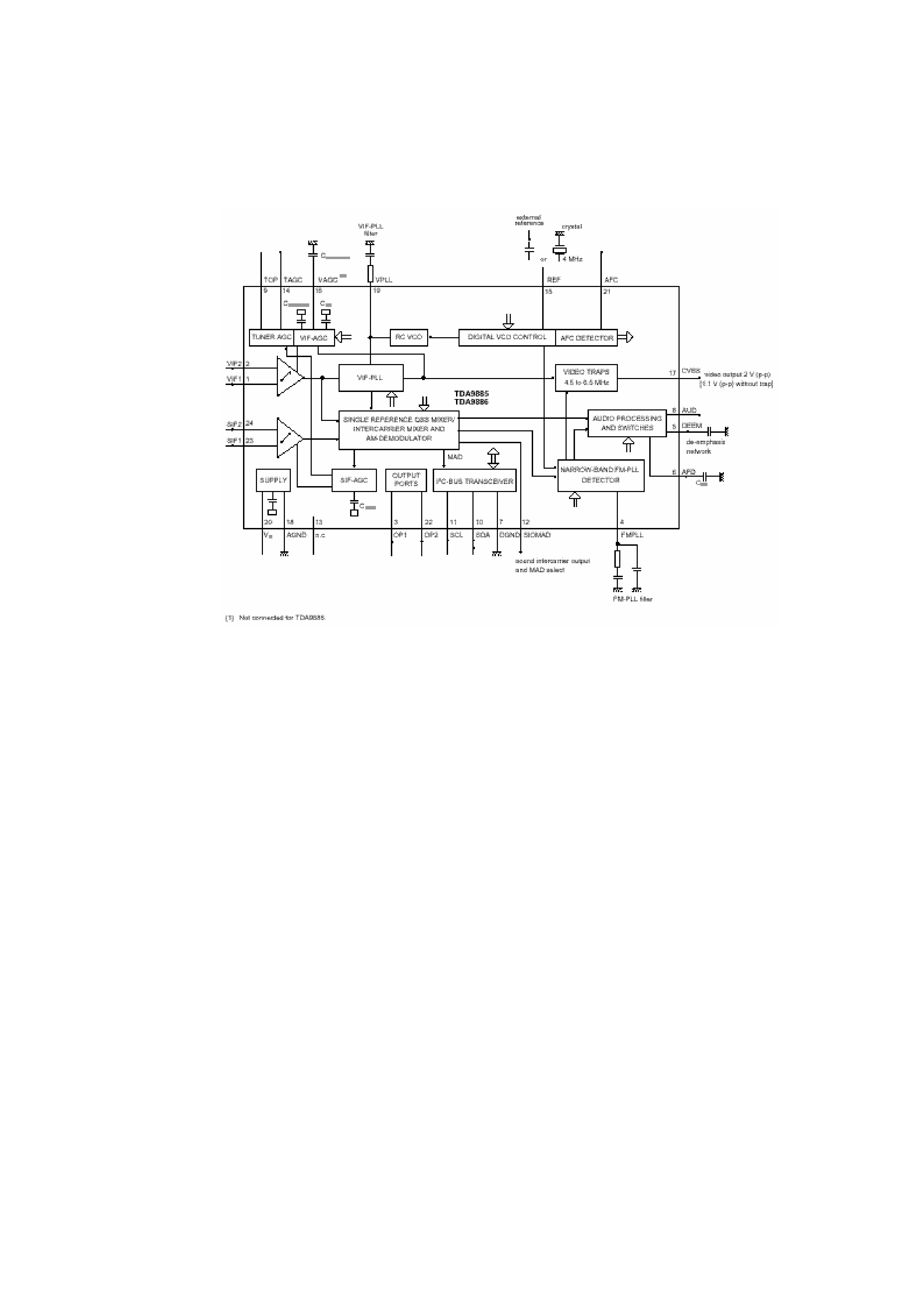
2
VIF amplifier, Tuner and VIF-AGC, VIF-AGC detector, Frequency Phase-Locked Loop (FPLL) detector, VCO
and divider, Digital acquisition help and AFC, Video demodulator and amplifier, Sound carrier trap, SIF
amplifier, SIF-AGC detector, Single reference QSS mixer, AM demodulator, FM demodulator and acquisition
help, Audio amplifier and mute time constant,
I²C-bus transceivers and MAD (module address), Internal
voltage stabilizer.
4. MULTI STANDARD SOUND PROCESSOR
The MSP34x1G family of single-chip Multistandard Sound Processors covers the sound processing of
all analog TV-Standards worldwide, as well as the NICAM digital sound standards. The full TV sound
processing, starting with analog sound IF signal-in, down to processed analog AF-out, is performed on
a single chip.
These TV sound processing ICs include versions for processing the multichannel television sound
(MTS) signal conforming to the standard recommended by the Broadcast Television Systems
Committee (BTSC). The DBX noise reduction, or alternatively, Micronas Noise Reduction (MNR) is
performed alignment free. Other processed standards are the Japanese FM-FM multiplex standard
(EIA-J) and the FM Stereo Radio standard.
Current ICs have to perform adjustment procedures in order to achieve good stereo separation for
BTSC and EIA-J. The MSP34x1G has optimum stereo performance without any adjustments.
5. 4.VIDEO SWITCH TEA6415
In case of three or more external sources are used, the video switch IC TEA6415 is used. The main
function of this device is to switch 8 video-input sources on the 6 outputs.
Each output can be switched on only one of each input. On each input an alignment of the lowest level
of the signal is made (bottom of sync. top for CVBS or black level for RGB signals).
Each nominal gain between any input and output is 6.5dB.For D2MAC or Chroma signal the alignment
is switched off by forcing, with an external resistor bridge, 5VDC on the input. Each input can be used
as a normal input or as a MAC or Chroma input (with external Resistor Bridge). All the switching
possibilities are changed through the BUS. Driving 75ohm load needs an external resistor. It is possible
to have the same input connected to several outputs.
6. AUDIO AMPLIFIER STAGE WITH TPA3002D2
The TPA3002D2 is a 9-W (per channel) efficient, Class-D audio amplifier for driving bridged-tied stereo
speakers. The TPA3002D2 can drive stereo speakersas low as 8
&. The high efficiency of the
TPA3002D2 eliminates the need for external heatsinks when playing music.