- 1 -
PP-2778L
Published by Service Dept.
Printed in Japan
Clarion Co., Ltd.
50 Kamitoda, Toda-shi, Saitama 335-8511 Japan
Service Dept.: 5-66 Azuma , Kitamoto-shi, Saitama 364-0007 Japan
Tel: +81-48-541-2335 / 2432 FAX: +81-48-541-2703
298-6307-00 Nov.2005
Service Manual
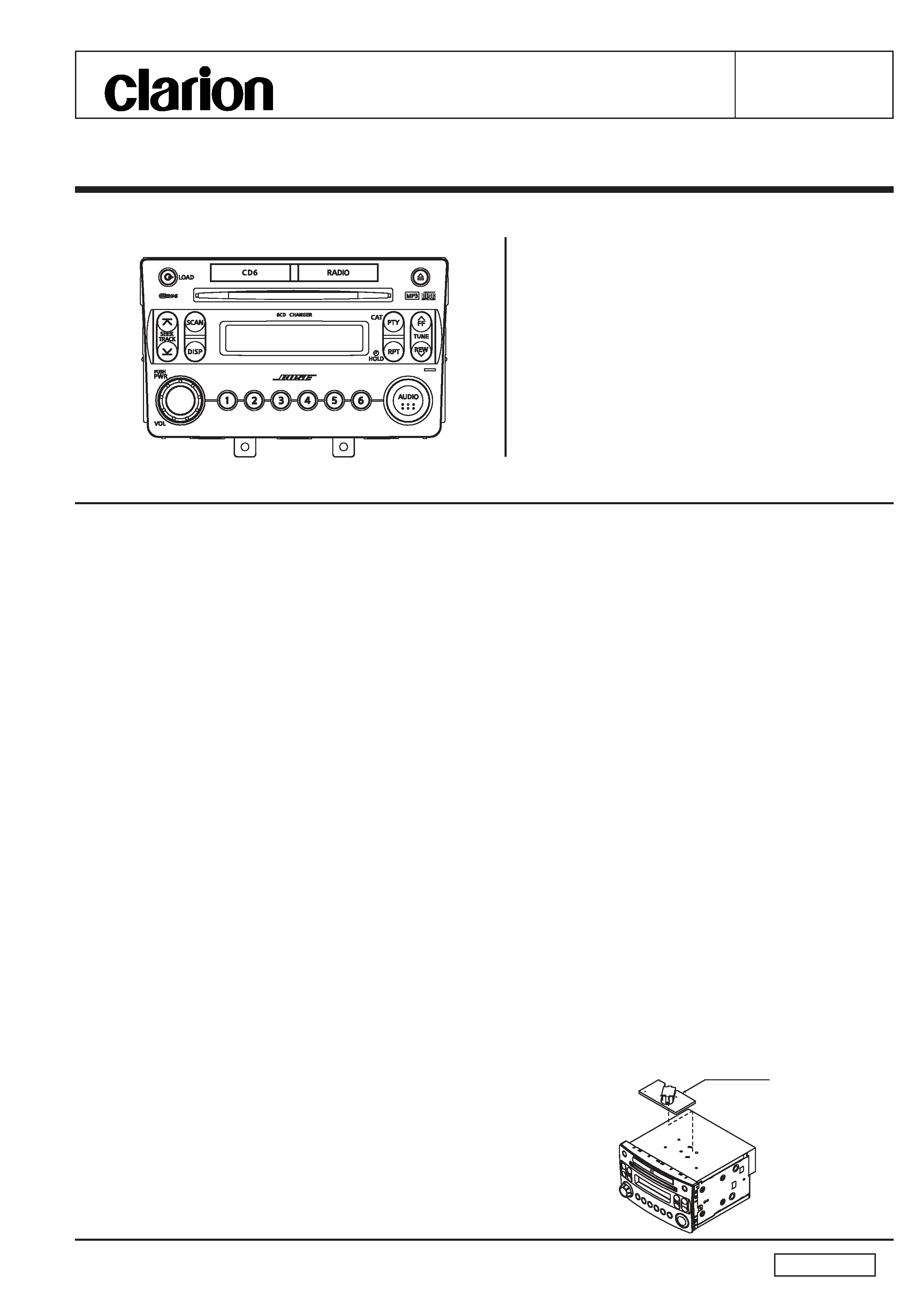
Model
NISSAN MOTOR Genuine
6-disc CD/MP3/WMA Autochanger
AM/FM Radio Stereo
PP-2778L
(Genuine No. 28185 CF50A)
(ID No. CY18B)
SPECIFICATIONS
Radio section
Tuning system:
PLL frequency synthesizer system
Receive range:
AM
530kHz to 1,710kHz
(10kHz STEP)
FM
87.75MHz(Display:87.7MHz)
to 107.9MHz
(200kHz STEP)
Intermediate frequency:
AM
450kHz
FM
10.7MHz
Quieting sensitivity:
AM
Less than 38dBu
FM
Less than 15dBu
Separation:
FM
22+5/-7dB(1kHz)
S/N ratio:
AM
More than 45dB
FM
More than 50dB
Auto tuning stop sensitivity:
AM
42+/-6dBu(600kHz)
39+/-6dBu(1,000/1,400kHz)
FM
32+/-6dBu
CD section
Mechanism:
6-disc CD autochanger
Disc:
12cm disc
Format:
CD-DA,MP3,WMA
Separation:
More than 60dB
(1kHz,20kHz L.P.F.)
S/N ratio:
More than 80dB(1kHz JIS-A)
Distortion:
Less than 0.1%(20kHz L.P.F.)
MP3/WMA operations: MP3 ; Sampling rate 8kHz - 48kHz
Bit rate : 8kbps - 320kbps / VBR
WMA;Bit rate;48kbps - 192kbps/VBR
Logical format(File system);
ISO9660 level 1, 2 or JOLIET or Romeo
General
Load impedance:
300 ohm/4ch
Power output:
6V x4
Power supply voltage: DC13.2V(10.8V to 15.6V)
Negative ground
Back-up consumption: Less than 1mA
Dimensions(mm):
180(W) x106.4(H) x167(D)
Weight:
Approx. 2.55kg
COMPONENT
PP-2778L-A
1.
Main unit
-----------
1
NOTES
*
Specifications and design are subject to change without
notice for further improvement.
*
We cannot supply PWB with component parts in prin-
ciple. When a circuit on PWB has failure, please repair it
by component parts base. Parts which are not mentioned
in service manual are not supplied.
*
This product includes technology owned by Microsoft
Corporation and cannot be used or distributed without a
license from MSLGP.
*
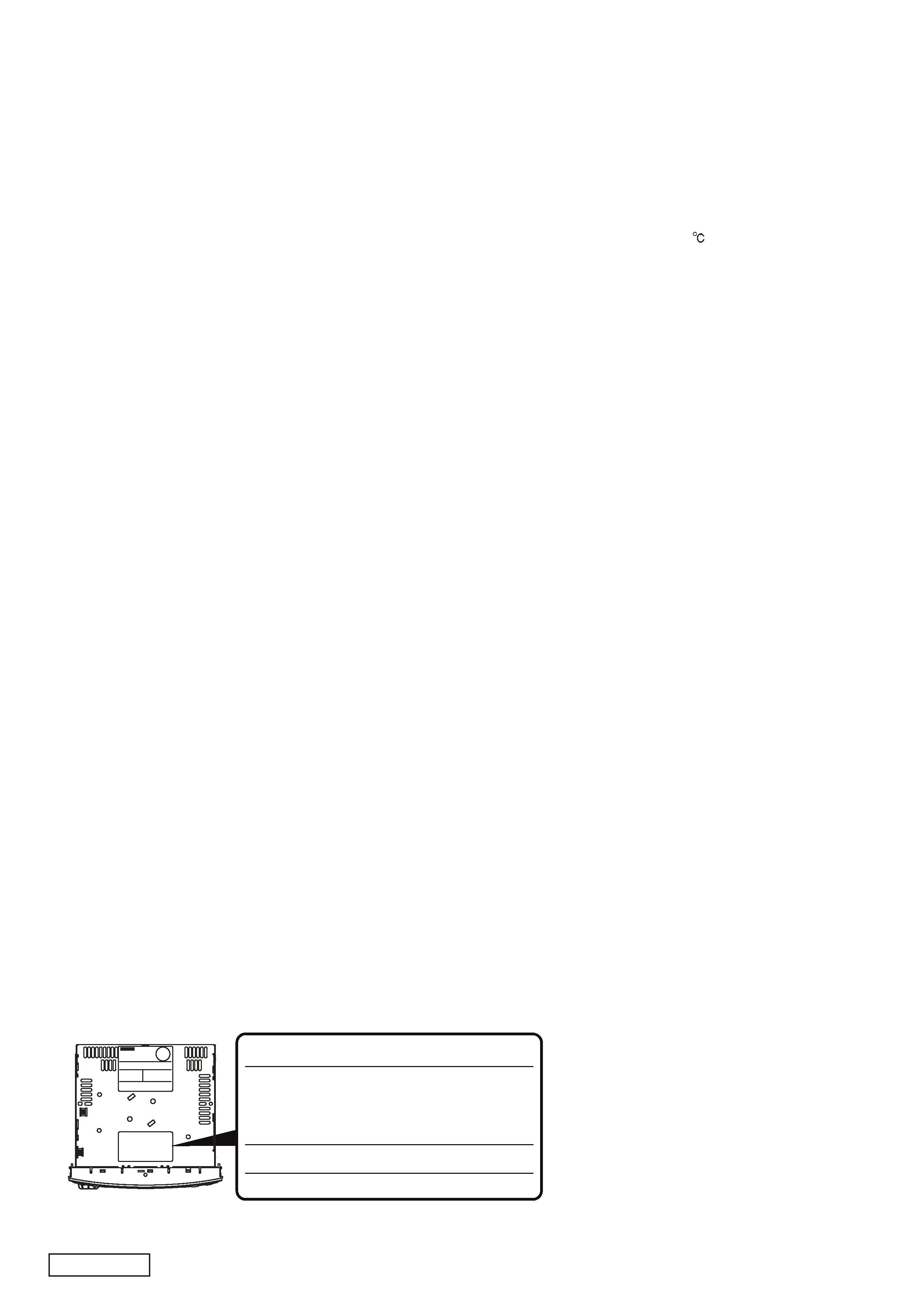
In case that the main unit or the CD changer mechanism
is transported for repair, the lock pin(966-0653-21) must
be set to fix the mechanism assy.
Lock pin
966-0653-21
- 2 -
PP-2778L
To engineers in charge of repair or
inspection of our products.
Before repair or inspection, make sure to follow the
instructions so that customers and Engineers in
charge of repair or inspection can avoid suffering
any risk or injury.
1. Use specified parts.
The system uses parts with special safety features against
fire and voltage. Use only parts with equivalent character-
istics when replacing them.
The use of unspecified parts shall be regarded as remod-
eling for which we shall not be liable. The onus of product
liability (PL) shall not be our responsibility in cases where
an accident or failure is as a result of unspecified parts
being used.
2. Place the parts and wiring back in their original positions
after replacement or re-wiring.
For proper circuit construction, use of insulation tubes,
bonding, gaps to PWB, etc, is involved. The wiring con-
nection and routing to the PWB are specially planned us-
ing clamps to keep away from heated and high voltage
parts. Ensure that they are placed back in their original
positions after repair or inspection.
If extended damage is caused due to negligence during
repair, the legal responsibility shall be with the repairing
company.
3. Check for safety after repair.
Check that the screws, parts and wires are put back se-
curely in their original position after repair. Ensure for safety
reasons there is no possibility of secondary ploblems
around the repaired spots.
If extended damage is caused due to negligence of repair,
the legal responsibility shall be with the repairing company.
4. Caution in removal and making wiring connection to the
parts for the automobile.
Disconnect the battery terminal after turning the ignition
key off. If wrong wiring connections are made with the bat-
tery connected, a short circuit and/or fire may occur. If ex-
tensive damage is caused due to negligence of repair, the
legal responsibility shall be with the repairing company.
5. Cautions regarding chips.
Do not reuse removed chips even when no abnormality is
observed in their appearance. Always replace them with
new ones. (The chip parts include resistors, capacitors,
diodes, transistors, etc). The negative pole of tantalum
capacitors is highly susceptible to heat, so use special care
when replacing them and check the operation afterwards.
6. Cautions in handling flexible PWB
Before working with a soldering iron, make sure that the
iron tip temperature is around 270 . Take care not to ap-
ply the iron tip repeatedly(more than three times)to the
same patterns. Also take care not to apply the tip with force.
7. Turn the unit OFF during disassembly and parts replace-
ment. Recheck all work before you apply power to the unit.
8. Cautions in checking that the optical pickup lights up.
The laser is focused on the disc reflection surface through
the lens of the optical pickup. When checking that the la-
ser optical diode lights up, keep your eyes more than 30cms
away from the lens. Prolonged viewing of the laser within
30cms may damage your eyesight.
9. Cautions in handling the optical pickup
The laser diode of the optical pickup can be damaged by
electrostatic charge caused by your clothes and body. Make
sure to avoid electrostatic charges on your clothes or body,
or discharge static electricity before handling the optical
pickup.
9-1. Laser diode
The laser diode terminals are shorted for transporta-
tion in order to prevent electrostatic damage. After
replacement, open the shorted circuit. When remov-
ing the pickup from the mechanism, short the termi-
nals by soldering them to prevent this damage.
9-2. Actuator
The actuator has a powerful magnetic circuit. If a
magnetic material is put close to it. Its characteris-
tics will change. Ensure that no foreign substances
enter through the ventilation slots in the cover.
9-3. Cleaning the lens
Dust on the optical lens affects performance. To
clean the lens, apply a small amount of isopropyl
alcohol to lens paper and wipe the lens gently.
CAUTION
Use of controls,adjustment,or performance of procedures
other than those specified herein,may result in hazardous
radiation exposure.
The compact disc player should not be adjusted or repaired
by anyone except properly qualified service personnel.
T H I S
P R ODUC T I O N
C O MP L I E S
W I T H
DHH S
R U L E S
2 1
C F R
S U B C H A P T E R
J
A P P L I CA B L E
A T
D A T E
O F
M AN UF ACTU RE .
I N T E RF ER EN C E
T H A T
M A Y
C AU SE
U N D E S I R E D
OP E R A T I O N .
TH I S
D E V I CE
C O M P L I ES
W I TH
P A RT
1 5
OF
TH E
F C C
RU L E S .
OP E R A T I O N
I S
S U B J E C T
T O
T H E
F O L L O W I N G
T W O
C O N D I T I O N S : ( 1 )
T H I S
D EV I C E
M AY
N O T
C A U SE
HA R M F U L
I N T E R F E RE N C E , A N D ( 2 )
T H I S
DE V I CE
M U S T
ACCE P T
AN Y
I N T E R F E RE N C E
R EC E I V E D , I N C L U D I N G
Th i s p r o d u c t
i nc l u de s t ec h n o l og y own ed by Mi c r os o f t Co r p o r a t i o n a nd
canno t b e u sed o r d i s t r i bu t ed w i t hou t a l i c e n s e f r om MSLGP .
Top view of the unit
Guide label
- 3 -
PP-2778L
ADJUSTMENTS
Item
Procedure
Measuring
instrument
Clock accuracy
1. Set a universal counter to TP101, adjust TC101 so that a reading of the counter
is 0+/-0.1 sec./day.
Universal counter
FM noise
convergence
1. Input the 98.1MHz/55dBu(1kHz,30% MOD)signal.(VOL MAX=0dB)
2. Adjust the outputs to -22dB by VR102 when the SG output is set -20dBu.
SSG
Milli-volt meter
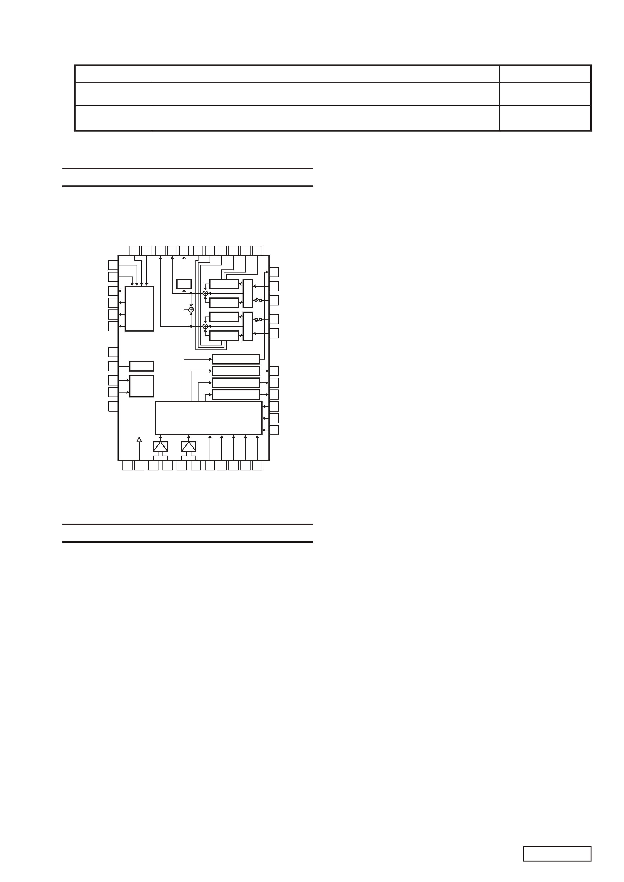
EXPLANATION OF IC
051-5041-90
BD3827K
Sound Processor
052-3193-10
M30624MGA-652GP
System Controller
Terminal Description
pin
1: LCD CLK
: O : The clock pulse output to the LCD driver.
pin
2: LCD DO
: O : The srial data output to the LCD driver.
pin
3: LCD DI
: IN : The srial data input from the LCD driver.
pin
4: ILL PULSE
: IN : Illumination control signal input.
pin
5: TIME BASE
: IN : Time base pulse input.
pin
6: BYTE
: IN : The data length selection(8bit/16bit).
pin
7: CN VSS
: IN : Connect to VSS via a resistor.
pin
8: TEST
: IN : For the test.
pin
9: NU
: O : Not in use.
pin 10: RESET
: IN : Reset signal input.
pin 11: X out
: O : Crystal connection.
pin 12: GND
: - : Ground.
pin 13: X in
: IN : Crystal connection.
pin 14: VDD
: - : Positive voltage supply.
pin 15: NMI
: IN : Connect to VDD via a resistor.
pin 16: BU DET
: IN : Backup detection signal input.
pin 17: ACC IN
: IN : ACC ON flag input.
pin 18: TEL ON
: IN : Telephone ON signal input.
pin 19: ILL ON
: IN : Illumination ON signal input.
pin 20: AMP ON
: O : Audio power amplifier ON signal output.
pin 21: SYS ON
: O : System ON signal output.
pin 22: DIMMER
: O : PWM output.
pin 23: NU
: O : Not in use.
pin 24: BEEP
: O : Beep out.
pin 25: TEL/NAVI MUTE: O : The muting signal output for the telephone
and the navigation.
pin 26: 6-CD REQ
: IN : The request signal input from the 6CD-
Changer.
pin 27: 6-CD RX
: IN : The serial data input for 6CD-Changer.
pin 28: 6-CD TX
: O : The serial data output for 6CD-Changer.
pin 29: NDS/FLASH TX : O : NDS serial data output for NDS and Flash
memory.
pin 30: NDS/FLASH RX : IN : NDS serial data input for NDS and Flash
memory.
pin 31: FLASH CLK
: O : The clock pulse output for the flash mem-
ory.
pin 32: NAVI ON
: IN : NAVI ON signal input.
pin 33: NU
: O : Not in use.
pin 34: NU
: O : Not in use.
pin 35: NDS CONT
: O : NDS/Automatic-changer select.
pin 36: NDS REQ 2
: IN : NDS request signal input.
pin 37: NDS REQ 1
: IN : NDS request signal input.
pin 38: SOURCE CHG : O : The signal source change signal output.
pin 39: FLASH EPM
: O : FLASH EPM.
pin 40: EEP ROM DO
: O : The serial data output to the EEP-ROM.
pin 41: EEP ROM CK
: O : The clock pulse output to the EEP-ROM.
pin 42: EEP ROM DI
: IN : The serial data input from the EEP-ROM.
pin 43: EEP ROM CE
: O : The chip enable signal output to the EEP-
ROM.
pin 44: FLASH CE
: IN : The chip enable signal input for the flash
memory.
pin 45: CD ON
: O : CD ON signal output.
pin 46: AUX REQ
: O : AUX request signal output.
pin 47: AUX ON
: IN : AUX ON signal input.
pin 48: COMBI ON
: O : Combi ON signal output.
pin 49: E VOL DO
: O : Serial data output to the volume IC.
pin 50: E VOL CLK
: O : The clock pulse output to the volume IC.
pin 51: Power IC SDA
: O : The serial data output to Power IC.
pin 52: Power IC CLK
: O : The clock pulse output to Power IC.
pin 53: Power IC Stndb : O : The standby signal output to Power IC.
pin 54: Power IC Diag
: IN : Power IC Diagnosis signal input.
pin 55: AF MUTE
: O : Audio frequency signal muting.
pin 56: VOL 1
: IN : Volume control pulse input from the rota-
ry encoder.
pin 57: VOL 2
: IN : Volume control pulse input from the rota-
ry encoder.
pin 58: NU
: O : Not in use.
pin 59: NU
: O : Not in use.
pin 60: VDD
: - : Positive voltage supply.
pin 61: NU
: O : Not in use.
pin 62: GND
: - : Ground.
pin 63: PLL CE
: O : The chip enable signal output to the PLL
IC.
pin 64: PLL CLK
: O : The clock pulse output to the PLL IC.
pin 65: PLL DO
: O : Serial data output to the PLL IC.
pin 66: PLL DI
: IN : Serial data input from the PLL IC.
pin 67: ST/TWEET
:I/O: Outputs "L" at AM 900kHz receiving. In-
puts "L" at FM stereo receiving.
pin 68: NU
: O : Not in use.
pin 69: NU
: O : Not in use.
pin 70: RDS DATA
: IN : RDS serial data input.
pin 71: RDS CLK
: O : RDS clock pulse output.
pin 72: VNC CNT
: O : VNC control signal output.
pin 73: MD LD
: IN : Disc-in signal input from the MD mecha-
nism.
36
Fout 2R
37
Fout 1R
39
Fout 1F
38
Fout 2F
40
VCC
41
ADJ
34
Fin 2F
35
Fin 1F
42
CLK
43
DATA
44
D GND
31
T
out
1
30
T
out
2
28
BP3-2
29
SW
Out
27
BP2-1
26
BP1-1
33
Fin
1R
32
Fin
2R
25
BP1-2
24
BP2-2
23
BP3-2
20
Vol 1
19
Sel 1
17
P out 1
18
P out 2
16
Sel 2
15
Vol 2
22
Loud 2
21
Loud 1
14 E 2
13 E 1
12 D 2
3
A
P
1
4
A
N
1
6
A
P
2
5
A
N
2
7
B
1
8
B
2
1
A
GND
2
FIL
9
C
1
10
C
2
11
D
1
+ -
+ -
Gain control
Gain control
Gain control
Gain control
V
o
lume
V
o
lume
BPF
Bas/Tre
BPF
Bas/Tre
Att
Fader
&
Volume
VCO
Logic
Input Selector
1/2Vcc
- 4 -
PP-2778L
pin 74: FAN ON
: O : The fan on signal output.
pin 75: MD 5V
: O : The power ON signal output for the MD
mechanism.
pin 76: MD WP
: O : Wake up signal output to the MD mecha-
nism.
pin 77: MD CS
: O : The chip selection signal output to the MD
mechanism.
pin 78: MD SCK
: O : The clock pulse output to the MD mech-
anism.
pin 79: MD SO
: O : Serial data output to the MD mechanism.
pin 80: MD RESET
: O : Reset pulse output to the MD mechanism.
pin 81: MD SRQ
: IN : Request signal input from the MD mech-
anism.
pin 82: MD SI
: IN : Serial data input from the MD mechanism.
pin 83: AREA 1
: IN : The destination setting input.
Refer Table 1.
pin 84: AREA 2
: IN : The destination setting input.
Refer Table 1.
pin 85: REMOTE SEL
: IN : L = Without Steering wheel remote con-
troller.
pin 86: CD CONNECT
: IN : CD connection check signal input.
pin 87: 6-CD LOAD
: IN : The loading control signal input for 6CD-
Changer.
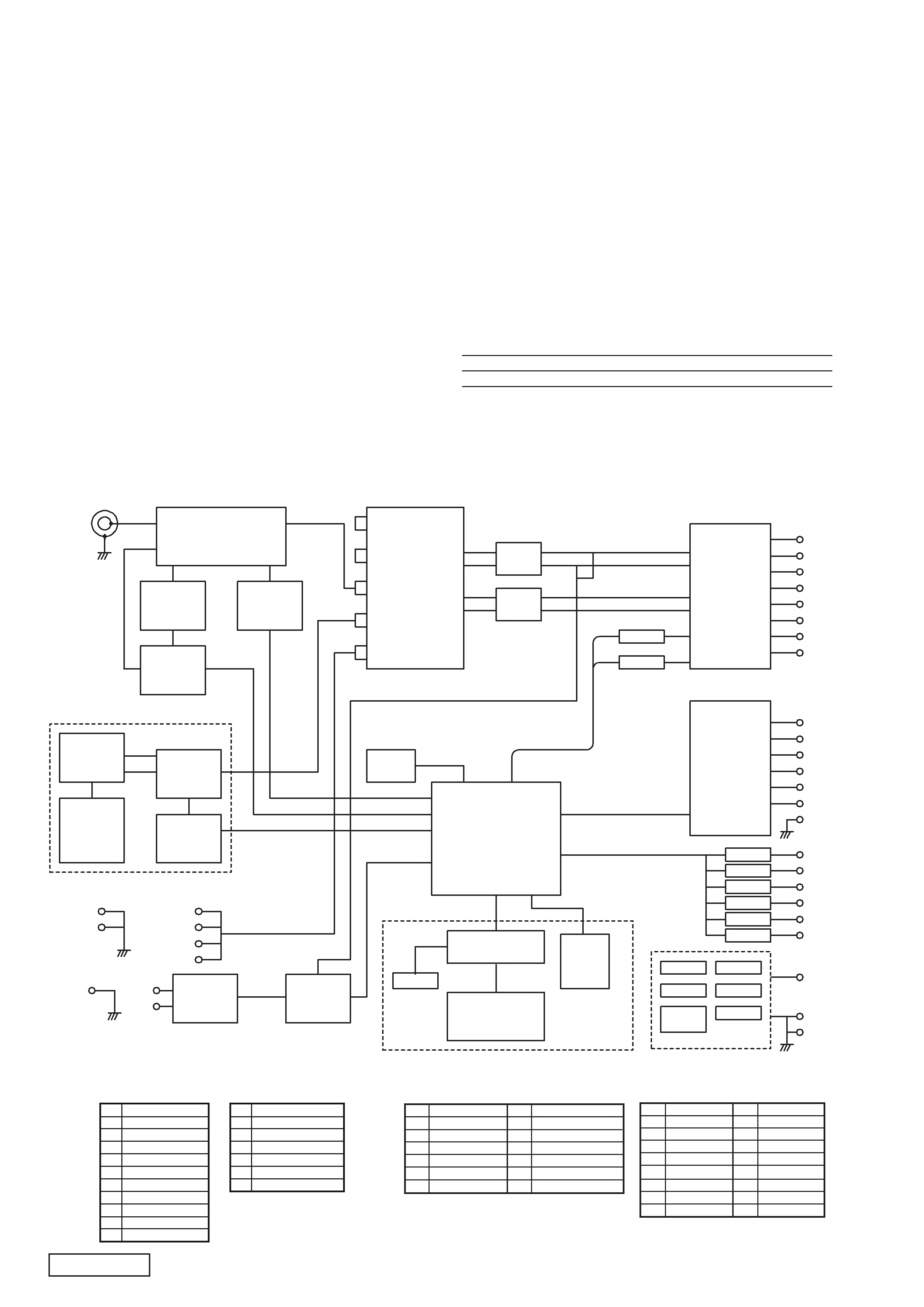
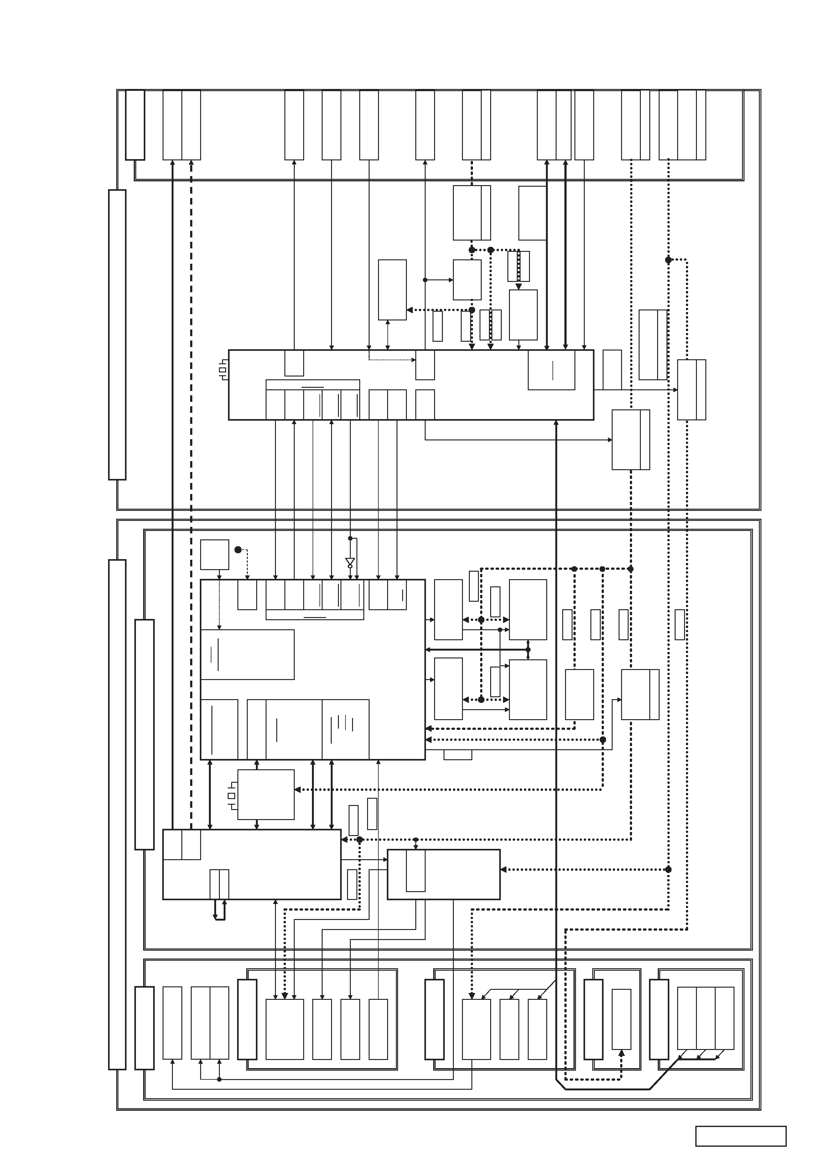
BLOCK DIAGRAM
Main section
pin 88: MD EJECT
: IN : MD eject switch signal input.
pin 89: 6CD EJECT
: IN : 6CD eject switch signal input.
pin 90: NU
: O : Not in use.
pin 91: NU
: O : Not in use.
pin 92: REM A
: IN : Remote control signal input.
pin 93: REM B
: IN : Remote control signal input.
pin 94: A VSS
: - : Negative voltage supply for analog section.
pin 95: NU
: O : Not in use.
pin 96: VREFI
: IN : The reference voltage input.
pin 97: A VDD
: - : Positive voltage supply for analog section.
pin 98: POWER SW
: IN : Power switch ON signal input.
pin 99: LCD RESET
: O : Reset pulse output to LCD.
pin100: LCD CE
: O : The chip enable signal output to the LCD
driver.
Table 1. The destination setting
Japan
NAM
GCC
AREA 1 ( pin 83 )
H
L
H
AREA 2 ( pin 84 )
H
H
L
ANT102
VNC
ANT-ON
AMP-ON
ACC
ILL-ON
ILL-
SYS-5V
SYS-9V
BL-9V
DIMMER
VDD
CD-9V
CD-5V
AM/FM-TUNER
PLL-IC
LC72191
ELECTRICAL
-VOLUME
VOLUME
BAL/FAD
POWER-IC
INTERFACE
M30624MGA
RESET
BL101
V01
V02
V03
V04
V05
V06
L.P.F
IC103
IC301
BASS/TREBLE
IC161
SAA6581
RF&CDIC
TC94A15F
DRIVER
SERVO
BD7961FM
DSP
CPU
IC203
BD5233G
NAVI-AMP
IC502
NAVI-MUTE
V34
V36
IC603
TDA8593J
BOSE
V
CH
STBY
BEEP
MUTE
POWER-SUPPLY
SYSTEM-CONTROL
(RADIO/6CD/CONTROL)
IC202
CD-CHANGER
or
SAT-RADIO
NAVI
REMOCON
V26
V27
V28
V08
V09
V10
V29
V35
RDS-DEC.
BD3827K
MUTE
LCD-DRIVER
LC75883
LCD
KEY
CD-LOAD
CD-EJ
VOL
PWR
V21
V33
IC1101
LCD1101
LUC1968A
880-1921O
CD CHANGER MODULE
TMS320DA140
M30621
NJM4565V
SWITCH PWB(B1)
E
A
F
B
N
O
P
L
G
K
D
C
I
H
J
M
FL
FR
RL
RR
No. Description
A
FRONT Lch(+)
B
FRONT Rch(+)
C
ILLUMI(+)
D
ACC
E
FRONT Lch(-)
F
FRONT Rch(-)
G
ANT. SIGNAL
H
BACK UP(+14V)
No. Description
K
AMP ON SIGNAL
L
REAR Rch(+)
M
GND
N
REAR Lch(-)
O
REAR Lch(+)
P
REAR Rch(-)
I
ILLUMI(-)
J
GND
A-16 MW
(Remote control)
A-12 MW
(NDS-Auto changer)
V21
V22
V23
V24
V25
V26
V27
V28
VNC-ON/OFF
N.C.
N.C.
N.C.
N.C.
REMO-A
REMO-B
NAVI-ON
V29
V30
V31
V32
V33
V34
V35
V36
REMO-GND
N.C.
N.C.
N.C.
GND
NAVI IN(-)
NAVI-GND
NAVI IN(+)
V01
V02
V03
V04
V05
V06
CD Lch(-)
CD Lch(+)
CD Rch(-)
CD Rch(+)
GND
Sheild-GND
V07
V08
V09
V10
V11
V12
N.C.
REQ(CD -> Combi)
RX(CD -> Combi)
TX(Combi -> CD)
N.C.
N.C.
No. Description
No. Description
No. Description
No. Description
NS10 MW
(Power/Front SP)
NS06 MW
(Rear SP)
- 5 -
PP-2778L
CD changer module section
AUDIO
L
,R
3mA
22mA
5mA
3mA
111mA
60mA
40mA
215mA
RF & CD
IC
TC94A15F
IC2
DSP
TMS320DA140
IC
9
MICOM
M30621
IC
3
EEPROM
(2K)
BR93L56RFVM
IC
4
VDDREF
3.3V Q
5
P-ON1
DSP
PWB
10MHz
SERVO DRIVER
BD7961FM
IC3
RESET BD5227G
IC
2
MOTOR DRIVER
IC1
IC6
SYS-ACC
TX
,RX
(SDA
,SCL)
ACC
3.3V
BA033SFP
IC6
DRIVER
PWB
PICK-UP
SPINDLE
MOTOR
SLED
MOTOR M3
M2
S3
MODE
MOTOR
V
MOTOR
LOADING
MOTOR
M1
V-
INT
SW
S2
MECH
SENSOR
PWB
DISC
SENSOR
PT3
PT6
MODE-
INT
SW
S1
IC5
MODE
SENSOR
PT1
V
SENSOR PT2
LED
PWB
(L
&
R)
LED
LED3
6
PON1
SHUT-SW
B/U-DET
25mA
PLAY
250mA
MECH
MOVE
1200mA
(MAX)
B/U-5V
VDD
3.3V
NJU7222U33
IC
5
SD-RAM
(64M)
K4S641632F
IC7
DECODE SN74LV139
IC4
FLASH
ROM
MBM29DL800BA
IC5
CLKIN 16.92MHz
AUDIO
L-CH
,R-CH
BUS0 BUS1 BUS2 BUS3 BUCK /CCE
SIGNAL
(INT) (INT) (INT)
DECODE
/
LATCH
74LV139
/74LV74
IC6
IC8
DAC
LRCKI/O
AUDIO
DATA(6)
BUS(6)
BCLKI/O DATAI/O
SENSOR
9V
Q
8
,Q
9
V-BUS
TX
A-MUTE
(TO
SET
U-COM)
LED-SW (PON3)
BUS
BUFFER FET
Q4
,Q6
,Q53
MECH
MODULE
CONNECTOR
(To
Main
Unit)
J3
DSP
1.6V
TPS76316DB
IC10
33mA
25mA
426mA
DRIVE
UNIT
LIMIT
SW
P-ON2
DRMUTE
LMT-SW
RESET
SERIAL
SERIAL
SERIAL
N-BUS (I2C)
CD
PWB
CCS
CSRQ
CMSI
CMSO
CSCK
CCS
CSRQ
CMSI
CMSO
CSCK
V-BUS
SFSY SBSY IPF
MBOV RESET
EMPHO
WUP
WUP
A-
MUTE
RESET
MODE
61mA
50mA
16.92MHz
JTAG
IEEE
1149.1
EMU0 EMU1 TCK
TCK_RET
TDO TDI TMS /TRST 3.3V GND
JTAG (15PIN)
EMPHI
170mA
45mA
33mA
426mA
MECH
MOVE
1200mA
(MAX)
PLAY
250mA
REQ
20
A
2.6
A
IC11
INV
RX3.3V 2SB1188
Q
2
111mA
SYSP
SYSCLK
IC12
INV
IC13
BUFF
INT
SERIAL
SERIAL
SERIAL
UART
ACC
5V
(PON1
CONT)
ACC
9V
(PON1
CONT)