PP-2665D-A
- 1 -
NISSAN Automobile Genuine
6-disc CD/MP3/WMA Autochanger
AM/FM Radio Stereo
PP-2665D-A
(Genuine No. 28185 AC705)
SPECIFICATIONS
Radio section
Tuning system:
PLL frequency synthesizer system
Receive range:
AM 530kHz to 1,710kHz
FM 87.75MHz to 107.9MHz
Intermediate frequency: AM 450kHz
FM 10.7MHz
Quieting sensitivity:
AM Less than 38dBu(at 20dB S/N)
FM Less than 15dBu(at 30dB S/N)
Separation:
FM 22+5/-7dB(1kHz)
Auto tuning stop sensitivity:
AM 42+/-6dBu(603kHz)
39+/-6dBu(999/1,404kHz)
FM 32+/-6dBu
CD section
Mechanism:
6-disc CD autochanger
Disc:
12cm disc
Format:
CD-DA,MP3,WMA
Separation:
More than 50dB(1kHz,20kHz
L.P.F.)
S/N ratio:
More than 74dB(1kHz JIS-A)
Distortion:
Less than 0.4%(20kHz L.P.F.)
General
Load impedance:
300 ohm/4ch
Power output:
6V x4
Power supply voltage:
DC13.2V(10.8V to 15.6V)
Negative ground
Back-up consumption: Less than 0.5mA
Dimensions(mm):
180(W)
106.4(H)
167(D)
Weight:
Approx. 3.5kg
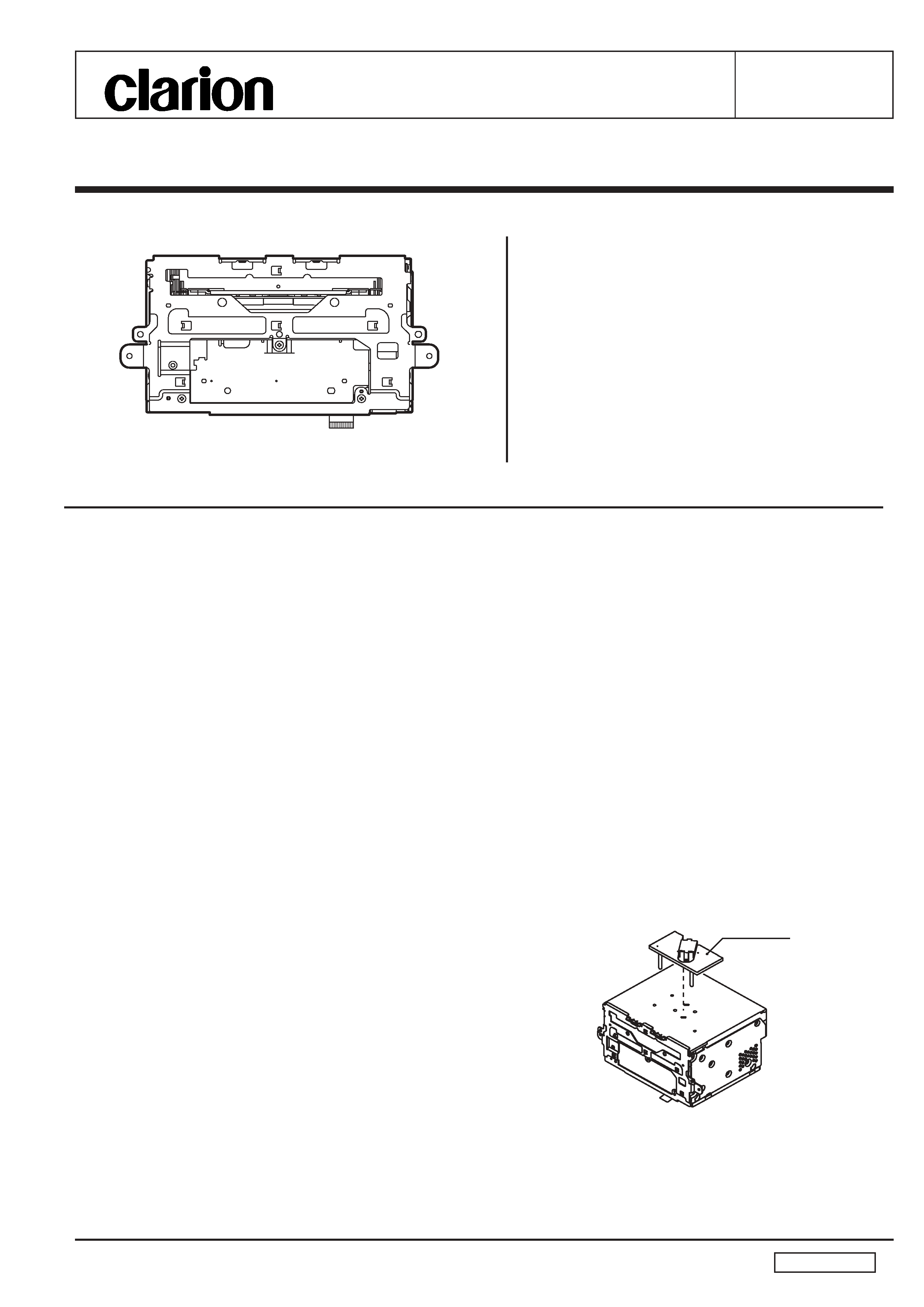
COMPONENTS
PP-2665D-A
1.
Main unit
-----------
1
NOTE
*
Specifications and design are subject to change without
notice for further improvement.
*
We cannot supply PWB with component parts in prin-
ciple. When a circuit on PWB has failure, please repair
it by component parts base. Parts which are not men-
tioned in service manual are not supplied.
*
This product includes technology owned by Microsoft
Corporation and cannot be used or distributed without a
license from MSLGP.
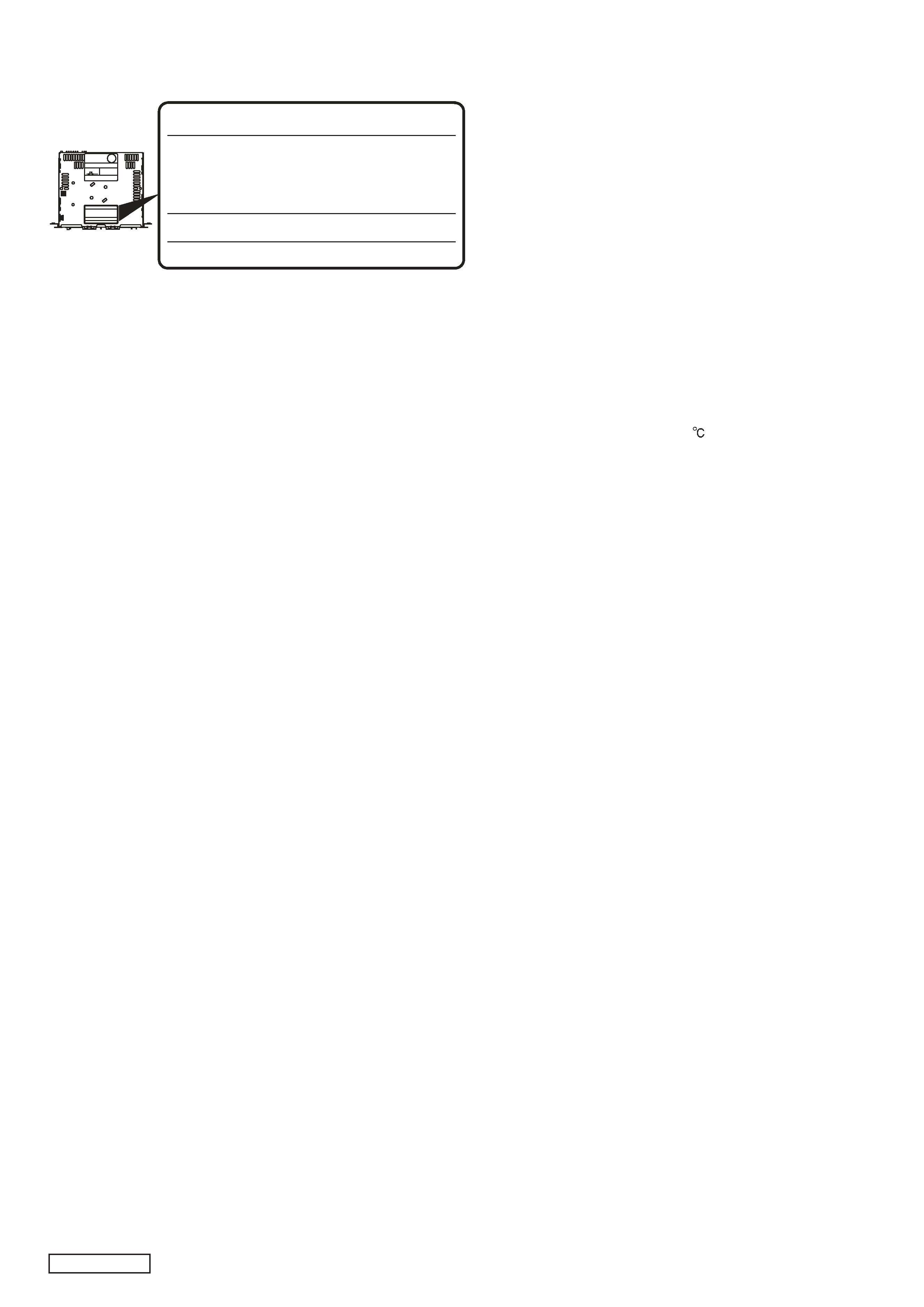
*
In case that the main unit or the CD changer mechanism
is transported for repair, the lock pin(966-0653-00) must
be set to fix the mechanism assy.
Published by Service Dept.
Printed in Japan
Clarion Co., Ltd.
50 Kamitoda, Toda-shi, Saitama 335-8511 Japan
Service Dept.: 5-66 Azuma , Kitamoto-shi, Saitama 364-0007 Japan
Tel: +81-48-541-2335 / 2432 FAX: +81-48-541-2703
298-6183-00 Oct.2004
Service Manual
Model
Lock pin
PP-2665D-A
- 2 -
To engineers in charge of repair or
inspection of our products.
Before repair or inspection, make sure to follow the
instructions so that customers and Engineers in
charge of repair or inspection can avoid suffering
any risk or injury.
1. Use specified parts.
The system uses parts with special safety features against
fire and voltage. Use only parts with equivalent character-
istics when replacing them.
The use of unspecified parts shall be regarded as remod-
eling for which we shall not be liable. The onus of product
liability (PL) shall not be our responsibility in cases where
an accident or failure is as a result of unspecified parts
being used.
2. Place the parts and wiring back in their original positions
after replacement or re-wiring.
For proper circuit construction, use of insulation tubes,
bonding, gaps to PWB, etc, is involved. The wiring con-
nection and routing to the PWB are specially planned us-
ing clamps to keep away from heated and high voltage
parts. Ensure that they are placed back in their original
positions after repair or inspection.
If extended damage is caused due to negligence during
repair, the legal responsibility shall be with the repairing
company.
3. Check for safety after repair.
Check that the screws, parts and wires are put back se-
curely in their original position after repair. Ensure for safety
reasons there is no possibility of secondary ploblems
around the repaired spots.
If extended damage is caused due to negligence of repair,
the legal responsibility shall be with the repairing company.
4. Caution in removal and making wiring connection to the
parts for the automobile.
Disconnect the battery terminal after turning the ignition
key off. If wrong wiring connections are made with the bat-
tery connected, a short circuit and/or fire may occur. If ex-
tensive damage is caused due to negligence of repair, the
legal responsibility shall be with the repairing company.
5. Cautions regarding chips.
Do not reuse removed chips even when no abnormality is
observed in their appearance. Always replace them with
new ones. (The chip parts include resistors, capacitors,
diodes, transistors, etc). The negative pole of tantalum
capacitors is highly susceptible to heat, so use special care
when replacing them and check the operation afterwards.
6. Cautions in handling flexible PWB
Before working with a soldering iron, make sure that the
iron tip temperature is around 270 . Take care not to ap-
ply the iron tip repeatedly(more than three times)to the
same patterns. Also take care not to apply the tip with force.
7. Turn the unit OFF during disassembly and parts replace-
ment. Recheck all work before you apply power to the unit.
8. Cautions in checking that the optical pickup lights up.
The laser is focused on the disc reflection surface through
the lens of the optical pickup. When checking that the la-
ser optical diode lights up, keep your eyes more than 30cms
away from the lens. Prolonged viewing of the laser within
30cms may damage your eyesight.
9. Cautions in handling the optical pickup
The laser diode of the optical pickup can be damaged by
electrostatic charge caused by your clothes and body. Make
sure to avoid electrostatic charges on your clothes or body,
or discharge static electricity before handling the optical
pickup.
9-1. Laser diode
The laser diode terminals are shorted for transporta-
tion in order to prevent electrostatic damage. After
replacement, open the shorted circuit. When remov-
ing the pickup from the mechanism, short the termi-
nals by soldering them to prevent this damage.
9-2. Actuator
The actuator has a powerful magnetic circuit. If a
magnetic material is put close to it. Its characteris-
tics will change. Ensure that no foreign substances
enter through the ventilation slots in the cover.
9-3. Cleaning the lens
Dust on the optical lens affects performance. To
clean the lens, apply a small amount of isopropyl
alcohol to lens paper and wipe the lens gently.
CAUTIONS
6. Cautions in handling flexible PWB
Before working with a soldering iron, make sure that the
iron tip temperature is around 270 . Take care not to ap-
ply the iron tip repeatedly(more than three times)to the
same patterns. Also take care not to apply the tip with force.
7. Turn the unit OFF during disassembly and parts replace-
ment. Recheck all work before you apply power to the unit.
8. Cautions in checking that the optical pickup lights up.
The laser is focused on the disc reflection surface through
the lens of the optical pickup. When checking that the la-
ser optical diode lights up, keep your eyes more than 30cms
away from the lens. Prolonged viewing of the laser within
30cms may damage your eyesight.
9. Cautions in handling the optical pickup
The laser diode of the optical pickup can be damaged by
electrostatic charge caused by your clothes and body. Make
sure to avoid electrostatic charges on your clothes or body,
or discharge static electricity before handling the optical
pickup.
9-1. Laser diode
The laser diode terminals are shorted for transporta-
tion in order to prevent electrostatic damage. After
replacement, open the shorted circuit. When remov-
ing the pickup from the mechanism, short the termi-
nals by soldering them to prevent this damage.
9-2. Actuator
The actuator has a powerful magnetic circuit. If a
magnetic material is put close to it. Its characteris-
tics will change. Ensure that no foreign substances
enter through the ventilation slots in the cover.
9-3. Cleaning the lens
Dust on the optical lens affects performance. To
clean the lens, apply a small amount of isopropyl
alcohol to lens paper and wipe the lens gently.
Use of controls,adjustment,or performance of procedures
other than those specified herein,may result in hazardous
radiation exposure.
The compact disc player should not be adjusted or repaired
by anyone except properly qualified service personnel.
T H I S
P R ODUC T I O N
C O MP L I E S
W I T H
DHH S
RU L E S
2 1
C F R
S U B C H A P T E R
J
A P P L I CA B L E
A T
D A T E
O F
M AN U F ACTU RE .
I N T E R F ER EN C E
T H A T
M A Y
C AU SE
U N D E S I R E D
OP E R A T I O N .
TH I S
D E V I CE
C O M P L I ES
W I TH
P A RT
1 5
O F
TH E
F C C
RU L E S .
OP E R A T I O N
I S
S U B J E C T
T O
T H E
F O L L O W I N G
T W O
C O N D I T I O N S : ( 1 )
T H I S
D EV I C E
M AY
N O T
C A U SE
HA R M F U L
I N T E R F E RE N C E , A N D ( 2 )
T H I S
DE V I CE
M U S T
ACCE P T
AN Y
I N T E R F E RE N C E
R EC E I V E D , I N C L U D I N G
Th i s p r o d u c t
i nc l u de s t ec h n o l og y own ed by Mi c r os o f t Co r p o r a t i o n a nd
cann o t be u s ed o r d i s t r i bu t ed w i t hou t a l i c en se f r om MSLGP .
Cl a r i o n
C o . , L t d
5 0
KA M I T O D A , T O D A
S H I , S A I T A M A
K E N , J A P AN
MO D E L
N O
12 V ( - ) G R O U N D
P/ N
F M : 8 7. 75 M H z - 1 0 7. 9M H z
M5
( F L A T
MA CHI NE S CRE W)
M A N U F A CT UR E D
8m m M A X
FR E Q U E N C Y
R A N G E
IS O
M O UN T
S CR E W
AM : 5 3 0 k H z - 1 7 1 0 k H z
S E RI A L
NO .
TH I S
P R O D U C TI O N
C O M P L I E S
WI TH
D H H S
R U L E S
2 1
C FR
SU BC H A PT ER
J
A P P L I C A BL E
A T
D AT E
O F
MA N U F A C T U R E .
I N T E R F ER EN C E
T H A T
M A Y
C AU S E
U N D E S I R E D
OP E R A T I O N .
TH I S
D E V I C E
C O M P L I E S
WI TH
P A R T
1 5
O F
TH E
F C C
R U L E S .
O PER AT I O N
I S
S U B J E C T
T O
T H E
F O L L O WI N G
T WO
C O N DI T I O N S : ( 1 )
T HI S
D E V I C E
M A Y
NO T
C A U S E
HA RM F U L
I N T E R F E RE NCE , A N D( 2 )
T H I S
DE V I CE
M U S T
A C CE P T
A N Y
I NT E R F E RE NC E
R E C E I V E D , I N CL UDI N G
Th i s pr oduc t
i n c l udes t e c h nol ogy owned b y Mi c r o s o f t
Co r p or at i o n a nd
c a nn ot
be us ed or
di s t r i bu t ed wi t hout
a l i c ens e f r om MSLGP.
NISSAN
Top view of the unit
Guide label
PP-2665D-A
- 3 -
ADJUSTMENTS
Checking the connection with
Switch-panel
When a switch-panel is correctly connected with the main unit,
ES-RETURN
terminal(pin 3) of a microcomputer(IC202) is
low
. When a switch-panel is incorrectly connected with the main unit, "ES-RETURN" line is cut, and BEEP sounds.
EXPLANATION OF IC
052-3161-50
M30624MGA-600GP
System Controller
Terminal Description
pin
1: WAKE UP
: IN : Wake up signal input.
pin
2: ACC ON
: O : ACC ON signal output.
pin
3: ES RETURN
: IN : The flexible PWB connection OK flag input.
pin
4: NU
: - : Not in use.
pin
5: NU
: - : Not in use.
pin
6: BYTE
: IN : The data length selection(8bit/16bit).
pin
7: CN VSS
: IN : Connect to VSS.
pin
8: TEST
: IN : For the test.
pin
9: NU
: - : Not in use.
pin 10: RESET
: IN : Reset signal input.
pin 11: X out
: O : Crystal connection.
pin 12: GND
: - : Ground.
pin 13: X IN
: IN : Crystal connection.
pin 14: VDD
: - : Positive voltage supply.
pin 15: NMI
: IN : Nonmaskable interrupt.
pin 16: BU DET
: IN : Backup detection signal input.
pin 17: ACC DET
: IN : ACC detection signal input.
pin 18: TEL ON
: IN : Telephone ON signal input.
pin 19: ILL DET
: IN : Illumination ON signal input.
pin 20: AMP ON
: O : Audio power amplifier ON signal output.
pin 21: SYS ON
: O : System ON signal output.
pin 22: VFD ON
: O : VFD ON signal output.
pin 23: NU
: - : Not in use.
pin 24: BEEP out
: O : Beep out.
pin 25: TEL/NAVI MUTE : O : The muting signal output for the telephone
and the navigation.
pin 26: 6-CD REQ
: IN : The request signal input from the 6CD-
Changer.
pin 27: 6-CD RX
: IN : The serial data input for 6CD-Changer.
pin 28: 6-CD TX
: O : The serial data output for 6CD-Changer.
pin 29: NDS/FLASH TX : O : The serial data output for NDS and Flash
memory.
pin 30: NDS/FLASH RX : IN : The serial data input for NDS and Flash
memory.
pin 31: FLASH CLK
: O : The clock pulse output for the flash mem-
ory.
pin 32: NAVI ON
: IN : NAVI ON signal input.
pin 33: ES TX
: O : Escutcheon serial data output.
pin 34: ES RX
: IN : Escutcheon serial data input.
pin 35: NDS A/C SEL
: O : NDS A/C selection signal output.
pin 36: NDS A/C REQ 2:IN : The request signal input from NDS A/C 2.
pin 37: NDS A/C REQ 1:IN : The request signal input from NDS A/C 1.
pin 38: NDS A/C A SEL: O : The audio signal selection command out-
put for NDS A/C.
pin 39: FLASH EPM
: O : FLASH EPM.
pin 40: EEP ROM DO
: O : The serial data output to the EEP-ROM.
pin 41: EEP ROM CK
: O : The clock pulse output to the EEP-ROM.
pin 42: EEP ROM DI
: IN : The serial data input from the EEP-ROM.
pin 43: EEP ROM CE
: O : The chip enable signal output to the EEP-
ROM.
pin 44: FLASH CE
: IN : The chip enable signal input for the flash
memory.
pin 45: CD ON
: O : CD ON signal output.
pin 46: AUX REQ
: O : AUX request signal output.
pin 47: AUX ON
: IN : AUX ON signal input.
pin 48: COMBI ON
: O : Combi ON flag output.
pin 49: E VOL DO
: O : Serial data output to the volume IC.
pin 50: E VOL CE
: O : Chip enable signal output to the volume IC.
pin 51: Power IC SDA
: O : The serial data output to Power IC.
pin 52: Power IC CLK
: O : The clock pulse output to Power IC.
pin 53: Power IC Stndb : O : The standby signal output to Power IC.
pin 54: Power IC Diag
: IN : Power IC Diagnosis signal input.
pin 55: NU
: - : Not in use.
pin 56: NU
: - : Not in use.
pin 57: NU
: - : Not in use.
pin 58: NU
: - : Not in use.
pin 59: NU
: - : Not in use.
pin 60: VDD
: - : Positive voltage supply.
pin 61: NU
: - : Not in use.
pin 62: GND
: - : Ground.
pin 63: PLL CE
: O : The chip enable signal output to the PLL
IC.
pin 64: PLL CLK
: O : The clock pulse output to the PLL IC.
pin 65: PLL DO
: O : Serial data output to the PLL IC.
pin 66: PLL DI
: IN : Serial data input from the PLL IC.
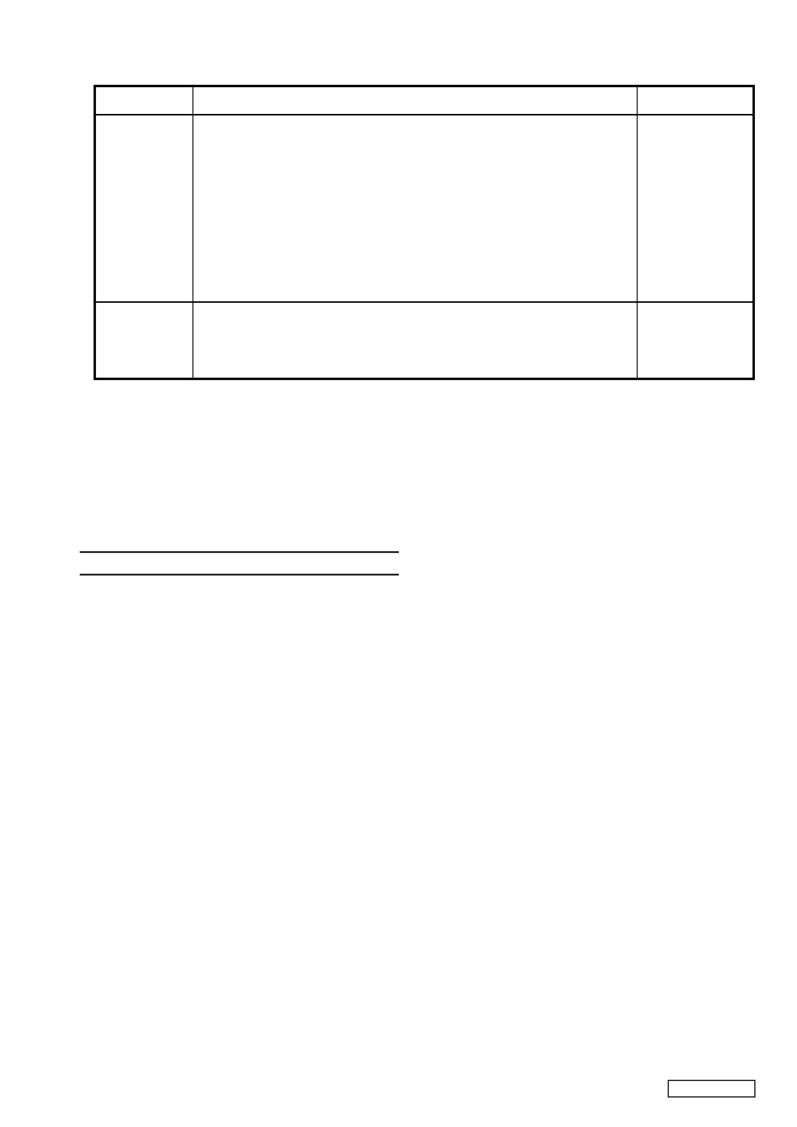
Item
Procedure
Measuring
instrument
Diversity
1. Turn off the unit, and continue pressing "DISP" button for several seconds.
(An antenna input was set main channel, and "MA" appears in the display.)
2. Set the volume to minimum.
3. Input a 98.1MHz/26dBu(1kHz,30%MOD) signal.
4. Connect a digital tester to TP101, and adjust VR101 so that the reading of the
digital tester becomes "high" from "low" exactly.
5. Set the SSG output to 22dBu, and confirm the reading of TP101 becomes "high"
from "low" within 3 seconds.
6. Set the SSG output to 30dBu, and confirm the voltage rage of TP101 is 10V from
2V.
7. Set the SSG output to 20dBu, and confirm the voltage of TP101 becomes less
than 1.0V within 5 seconds.
1. Set an antenna input to main channel.
2. Input a 98.1MHz/55dBu(1kHz,30%MOD) signal, and set the output power of the
unit to 1.4V(= 0dB).
3. Adjust VR102 so that the noise level becomes -22dB.
SSG
Digital tester
Oscilloscope
SSG
Digital tester
Noise
Convergence

PP-2665D-A
- 4 -
pin 67: ST/TWEET
:I/O: Outputs "L" at AM 900kHz receiving. Inputs
"L" at FM stereo receiving.
pin 68: NU
: - : Not in use.
pin 69: NU
: - : Not in use.
pin 70: RDS DATA
: IN : RDS serial data input.
pin 71: RDS CLK
: O : RDS clock pulse output.
pin 72: Speed Pulse
: IN : Speed pulse input.
pin 73: MD LD
: IN : Disc-in signal input from the MD mecha-
nism.
pin 74: FAN ON
: O : The fan on signal output.
pin 75: MD 5V
: O : The power ON signal output for the MD
mechanism.
pin 76: MD WP
: O : Wake up signal output to the MD mecha-
nism.
pin 77: MD CS
: O : The chip selection signal output to the MD
mechanism.
pin 78: MD SCK
: O : The clock pulse output to the MD mecha-
nism.
pin 79: MD SO
: O : Serial data output to the MD mechanism.
pin 80: MD RESET
: O : Reset pulse output to the MD mechanism.
pin 81: MD SRQ
: IN : Request signal input from the MD mecha-
nism.
pin 82: MD SI
: IN : Serial data input from the MD mechanism.
pin 83: AREA 1
: IN : The destination setting input.
pin 84: AREA 2
: IN : The destination setting input.
pin 85: 160W / BOSE
: IN : The initial setting terminal. Low = BOSE.
pin 86: CD CONNECT
: IN : CD connection check signal input.
pin 87: NU
: - : Not in use.
pin 88: NU
: - : Not in use.
pin 89: NU
: - : Not in use.
pin 90: NU
: - : Not in use.
pin 91: NU
: - : Not in use.
pin 92: HAND REM A
: IN : Steering wheel remote controller input.
pin 93: HAND REM B
: IN : Steering wheel remote controller input.
pin 94: A VSS
: - : Negative voltage supply for analog section.
pin 95: S METER
: IN : The input terminal of internal A/D convert-
er to monitor the radio field strength.
pin 96: Vref
: - : Reference voltage.
pin 97: A VDD
: - : Positive voltage supply for analog section.
pin 98: NU
: - : Not in use.
pin 99: NU
: - : Not in use.
pin100: NU
: - : Not in use.
052-5061-01
M30621MCM-4S5GP
Mechanism Controller
[NOTE] This IC is compatible with 052-5061-00.
Terminal Description
pin
1: HSSW1
: IN : L = It operates by one twice the speed of
a standard.
pin
2: NU
: - : Not in use.
pin
3: NU
: - : Not in use.
pin
4: NU
: - : Not in use.
pin
5: NU
: - : Not in use.
pin
6: CN VSS
: IN : Connect to VSS.
pin
7: NU
: - : Not in use.
pin
8: NU
: - : Not in use.
pin
9: RESET
: IN : Reset signal input.
pin 10: X out
: O : Crystal connection.
pin 11: VSS
: - : Negative voltage supply.
pin 12: X IN
: IN : Crystal connection.
pin 13: VDD
: - : Positive voltage supply.
pin 14: NMI
: IN : Not in use.
pin 15: NU
: - : Not in use.
pin 16: ACC DET
: IN : ACC detection signal input.
pin 17: BU DET
: IN : Backup detection signal input.
pin 18: PON 2
: O : Power ON signal output.
pin 19: NU
: - : Not in use.
pin 20: NDS REQ
: O : NDS request signal output.
pin 21: NU
: - : Not in use.
pin 22: NDS RX
: IN : NDS serial data input.
pin 23: NDS TX
: O : NDS serial data output.
pin 24: T DATA
: O : The display data output for the test mode
indication.
pin 25: T CLK
: O : The test clock output.
pin 26: Flash Write Set : IN : The flash memory writing mode setting in-
put.
pin 27: DSP V-BUS CS : O : DSP V-BUS Chip Select.
pin 28: DSP V-BUS DO : O : DSP V-BUS Data Output.
pin 29: DSP V-BUS DI : IN : DSP V-BUS Data Input.
pin 30: DSP V-BUS CK : O : DSP V-BUS Clock output.
pin 31: V-BUS SRQ
: IN : V-BUS Slave request.
pin 32: SW 1
: IN : The switch signal input.
pin 33: SW 2
: IN : The switch signal input.
pin 34: EPM
: IN : The flash memory control setting.
pin 35: PT 2
: IN : The photo sensor signal input.
pin 36: PT 5
: IN : The photo sensor signal input.
pin 37: PT 4
: IN : The photo sensor signal input.
pin 38: PT 3
: IN : The photo sensor signal input.
pin 39: ROM Correct
: IN : ROM correction control signal input.
pin 40: PT 6
: IN : The photo sensor signal input.
pin 41: SW 9V
: O : 9V power supply control.
pin 42: PT 1
: IN : The photo sensor signal input.
pin 43: LM CCW
: O : Loading motor control output.
pin 44: LM CW
: O : Loading motor control output.
pin 45: VM CCW
: O : V motor control output.
pin 46: VM CW
: O : V motor control output.
pin 47: MM CCW
: O : Mode motor control output.
pin 48: MM CW
: O : Mode motor control output.
pin 49: D MUTE
: O : Digital mute signal output.
pin 50: DSP RESET
: O : Reset signal output to the DSP IC.
pin 51: DSP Wakeup
: O : DSP wakeup command output.
pin 52: TEST 4
: IN : For the test.
pin 53: TEST 3
: IN : For the test.
pin 54: TEST 2
: IN : For the test.
pin 55: TEST 1
: IN : For the test.
pin 56: EEP DI
: IN : The serial data input from the EEP-ROM.
pin 57: EEP DO
: O : The serial data output to the EEP-ROM.
pin 58: EEP CLK
: O : The clock pulse output to the EEP-ROM.
pin 59: EEP CE
: O : The chip enable signal output to the EEP-
ROM.
pin 60: OEM SW 1
: IN : The destination setting.
pin 61: OEM SW 2
: IN : The destination setting.
pin 62: A MUTE
: O : The audio mute signal output.
pin 63: NU
: - : Not in use.
pin 64: NU
: - : Not in use.
pin 65: NU
: - : Not in use.
pin 66: SHUT
: IN : The shutter signal input.
pin 67: P ON 1
: O : Power ON signal output.
pin 68: NU
: - : Not in use.
pin 69: NU
: - : Not in use.
pin 70: NU
: - : Not in use.
pin 71: NU
: - : Not in use.
pin 72: NU
: - : Not in use.
pin 73: NU
: - : Not in use.
pin 74: NU
: - : Not in use.
pin 75: A VSS
: - : Negative voltage supply for analog section.
pin 76: NU
: - : Not in use.
pin 77: Vref
: - : Reference voltage.
pin 78: A VCC
: - : Positive voltage supply for the internal an-
alog section.
pin 79: T CLK
: O : "Test mode display" clock output.
pin 80: NU
: - : Not in use.
PP-2665D-A
- 5 -
17
15
18
19
26
27
28
31
35
33
22
16
21
20
24
25
23
30
34
32
25k
25k
25k
25k
3
4
A in L+
A in L-
7
9
11
13
14
12
10
8
B in L
C in L
D in L
E in L
E in R
D in R
C in R
B in R
Volume
Bass/Tre
B.P.F.
37
39
29 Sub Woofer
Volume
Bass/Tre
B.P.F.
25k
25k
25k
25k
Sub Woof
control
A in R-
A in R+
5
6
36
38
P
out
L
Sel
out
L
V
ol
in
L
Loud
L
BPF
1
L
BPF
2
L
BPF
3
L
T
out
L
Fed
in
Rear
L
Fed
in
Frnt
L
Fed out Frnt L
Fed out Rear L
Fed out Rear R
Fed out Frnt R
P
out
R
Sel
out
R
V
ol
in
R
Loud
R
BPF
1
R
BPF
2
R
BPF
3
R
T
out
R
Fed
in
Rear
R
Fed
in
Frnt
R
42
43
Clock in
Data in
Logic
40
41
VCC
ADJ
VCO
2
FIL
44 Digital Ground
1
Analog
Ground
051-5037-90
BD3807K
Audio signal processor
Terminal Description
pin
1: A GND
: Analog ground.
pin
2: FIL
: VCC/2.
pin
3: A in L+
: A Non-iverted input, Left channel.
pin
4: A in L-
: A Inverted input, Left channel.
pin
5: A in R-
: A Inverted input, Right channel.
pin
6: A in R+
: A Non-iverted input, Right channel.
pin
7: B in L
: B Input, Left channel.
pin
8: B in R
: B Input, Right channel.
pin
9: C in L
: C Input, Left channel.
pin 10: C in R
: C Input, Right channel.
pin 11: D in L
: D Input, Left channel.
pin 12: D in R
: D Input, Right channel.
pin 13: E in L
: E Input, Left channel.
pin 14: E in R
: E Input, Right channel.
pin 15: P out L
: Input-gain ouput, Left channel.
pin 16: P out R
: Input-gain ouput, Right channel.
pin 17: SEL out L
: Input-gain ouput, Left channel.
pin 18: VOL in L
: Volume Input, Left channel.
pin 19: LOUD L
: Loudness setting, Left channel.
pin 20: LOUD R
: Loudness setting, Right channel.
pin 21: VOL in R
: Volume Input, Right channel.
pin 22: SEL out R
: Input-gain ouput, Right channel.
pin 23: BPF 3 R
: General-purpose BPF setting 3, Right channel.
pin 24: BPF 1 R
: General-purpose BPF setting 1, Right channel.
pin 25: BPF 2 R
: General-purpose BPF setting 2, Right channel.
pin 26: BPF 1 L
: General-purpose BPF setting 1, Left channel.
pin 27: BPF 2 L
: General-purpose BPF setting 2, Left channel.
pin 28: BPF 3 L
: General-purpose BPF setting 3, Left channel.
pin 29: Sub Woofer
: Sub-woofer output.
pin 30: Tone out R
: Tone controller output, Right channel.
pin 31: Tone out L
: Tone controller output, Left channel.
pin 32: Fed in Rear R : Right channel Rear Input.
pin 33: Fed in Rear L : Left channel Rear Input.
pin 34: Fed in Frnt R : Right channel Front Input.
pin 35: Fed in Frnt L
: Left channel Front Input.
pin 36: Fed out Rea R : Right channel Rear output.
pin 37: Fed out Rea L : Left channel Rear output.
pin 38: Fed out Frn R : Right channel Front output.
pin 39: Fed out Frn L : Left channel Front output.
pin 40: VCC
: Power supply.
pin 41: ADJ
: VCO frequency adjust.
pin 42: CLK
: The clock pulse.
pin 43: DATA
: The serial data.
pin 44: D GND
: Digital ground.
pin 30: Tone out R
: Tone controller output, Right channel.
pin 31: Tone out L
: Tone controller output, Left channel.
pin 32: Fed in Rear R : Right channel Rear Input.
pin 33: Fed in Rear L : Left channel Rear Input.
pin 34: Fed in Frnt R : Right channel Front Input.
pin 35: Fed in Frnt L
: Left channel Front Input.
pin 36: Fed out Rea R : Right channel Rear output.
pin 37: Fed out Rea L : Left channel Rear output.
pin 38: Fed out Frn R : Right channel Front output.
pin 39: Fed out Frn L : Left channel Front output.
pin 40: VCC
: POower supply.
pin 41: ADJ
: VCO frequency adjust.
pin 42: CLK
: The clock pulse.
pin 43: DATA
: The serial data.
pin 44: D GND
: Digital ground.
052-5062-02
MBM29DL800BA-90PFTN
8 M bit Flash Memory
[NOTE] This IC is compatible with 052-5062-01.
Terminal Description
pin
1: Address 15
: IN : Address signal input.
pin
2: Address 14
: IN : Address signal input.
pin
3: Address 13
: IN : Address signal input.
pin
4: Address 12
: IN : Address signal input.
pin
5: Address 11
: IN : Address signal input.
pin
6: Address 10
: IN : Address signal input.
pin
7: Address 9
: IN : Address signal input.
pin
8: Address 8
: IN : Address signal input.
pin
9: NU
: - : Not in use.
pin 10: NU
: - : Not in use.
pin 11: WE
: IN : Write enable signal input.
pin 12: RESET
: IN : Reset signal input.
pin 13: NU
: - : Not in use.
pin 14: NU
: - : Not in use.
pin 15: Ready/Busy
: O : Ready/Busy flag output, H = Ready.
pin 16: Address 18
: IN : Address signal input.
pin 17: Address 17
: IN : Address signal input.
pin 18: Address 7
: IN : Address signal input.
pin 19: Address 6
: IN : Address signal input.
pin 20: Address 5
: IN : Address signal input.
pin 21: Address 4
: IN : Address signal input.
pin 22: Address 3
: IN : Address signal input.
pin 23: Address 2
: IN : Address signal input.
pin 24: Address 1
: IN : Address signal input.
pin 25: Address 0
: IN : Address signal input.
pin 26: CE
: IN : Chip enable signal input.
pin 27: VSS
: - : Negative supply voltage.
pin 28: OE
: IN : Output enable signal input.
pin 29: DQ 0
:I/O: The data input / output.
pin 30: DQ 8
:I/O: The data input / output.
pin 31: DQ 1
:I/O: The data input / output.
pin 32: DQ 9
:I/O: The data input / output.
pin 33: DQ 2
:I/O: The data input / output.
pin 34: DQ 10
:I/O: The data input / output.
pin 35: DQ 3
:I/O: The data input / output.
pin 36: DQ 11
:I/O: The data input / output.
pin 37: VCC
: - : Positive supply voltage.
pin 38: DQ 4
:I/O: The data input / output.
pin 39: DQ 12
:I/O: The data input / output.
pin 40: DQ 5
:I/O: The data input / output.
pin 41: DQ 13
:I/O: The data input / output.
pin 42: DQ 6
:I/O: The data input / output.
pin 43: DQ 14
:I/O: The data input / output.
pin 44: DQ 7
:I/O: The data input / output.
pin 45: DQ 15/A-1
:I/O: The data input/output,TheAddress signal
input.
pin 46: VSS
: - : Negative supply voltage.
pin 47: BYTE
: IN : The data length selection(8bit/16bit).
pin 48: Address 16
: IN : Address signal input.