PN-2871F, L, R
PP-2871H, N, T
- 1 -
Service Manual
Published by Service Dept.
Printed in Japan
Clarion Co., Ltd.
7-2, Shintoshin, Chuo-ku, Saitama-shi, Saitama 330-0081 Japan
Service Dept.: 7-2, Shintoshin, Chuo-ku, Saitama-shi, Saitama 330-0081 Japan
Tel: +81-48-601-3705 FAX: +81-48-601-3804
298-6510-00 Nov.2007
NISSAN Automobile Genuine
AM/FM Radio CD Combination
PN-2871F-A,B
PN-2871L-A,B,C,E,F,G
PN-2871R-A
PP-2871H-A,B,C
PP-2871N-A,B
PP-2871T-A,B,C,D,E,F
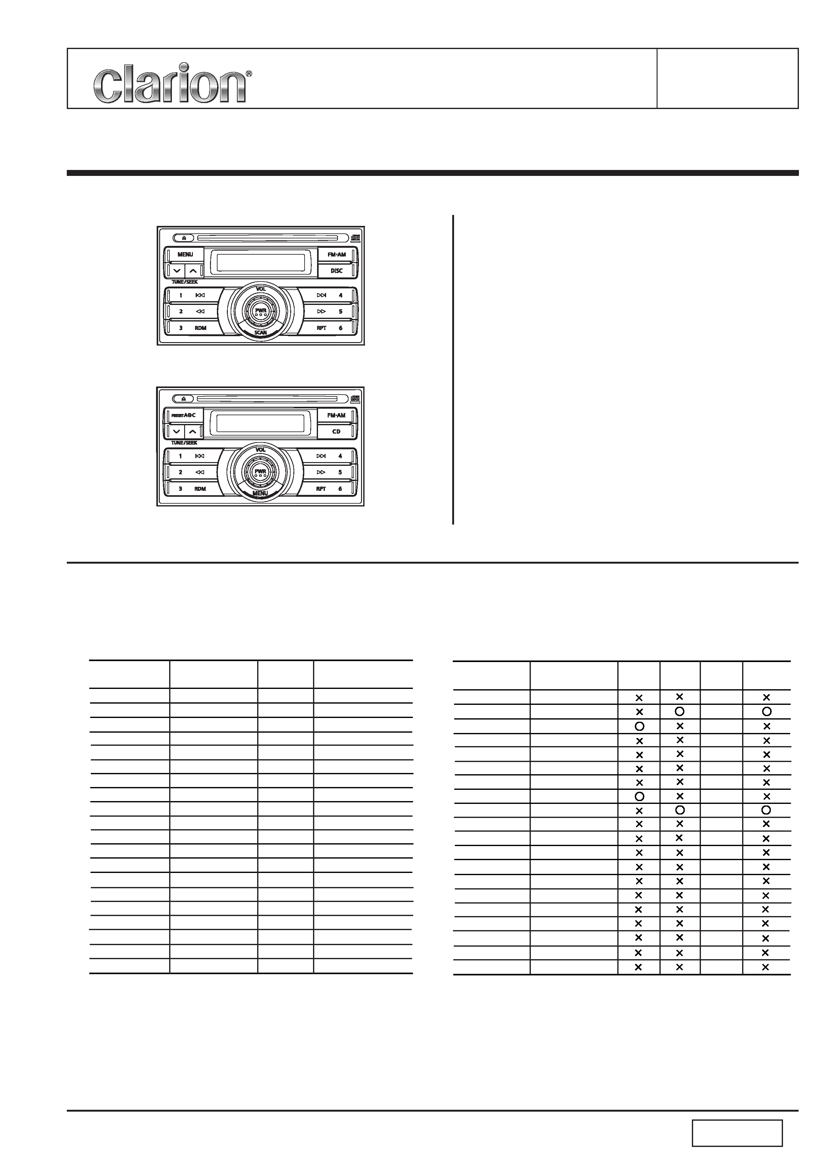
DIFFERENCES
Model
Model
Model
Model
Model
Model
PN-2871F-A, B, PN-2871L-B, C, E, F, PN-2871R-A
PP-2871H-A, B, C, PP-2871N-A, B
PP-2871T-A, B, C, D
PN-2871L-A, G
TEL
line in
ANT
Model
Illumi
control
Remote
control
Illumination
color
PN-2871F-A
PN-2871F-B
PN-2871L-A
PN-2871L-B
PN-2871L-C
PN-2871L-E
PN-2871L-F
PN-2871L-G
PN-2871R-A
PP-2871H-A
PP-2871H-B
PP-2871H-C
PP-2871N-A
PP-2871N-B
PP-2871T-A
PP-2871T-B
PP-2871T-C
PP-2871T-D
PP-2871T-E
PP-2871T-F
Reddish orange
Reddish orange
Yellow orange
Yellow orange
Yellow orange
Yellow orange
Yellow orange
Yellow orange
Yellow orange
Yellow orange
Reddish orange
Reddish orange
Yellow orange
Yellow orange
Reddish orange
Reddish orange
Reddish orange
Reddish orange
Reddish orange
Reddish orange
Glass
Glass
Glass
Glass
Glass
Glass
Glass
Glass
Glass
Pole
Pole
Pole
Pole
Pole
Glass
Glass
Glass
Glass
Glass
Glass
Model
Genuine No.
ID No.
Distination
PN-2871F-A
PN-2871F-B
PN-2871L-A
PN-2871L-B
PN-2871L-C
PN-2871L-E
PN-2871L-F
PN-2871L-G
PN-2871R-A
PP-2871H-A
PP-2871H-B
PP-2871H-C
PP-2871N-A
PP-2871N-B
PP-2871T-A
PP-2871T-B
PP-2871T-C
PP-2871T-D
PP-2871T-E
PP-2871T-F
28185 JD10A
28185 JE21A
28185 EM31A
28185 EL00A
28185 EE51A
28185 EF81A
28185 EE91A
28185 EM32A
28185 EW80A
28185 EB700
28185 VM00G
28185 VM00C
28185 CJ90A
28185 CJ40A
28185 JH40A
28185 JH40A
28185 JH40A
28185 JH40B
28185 JH40B
28185 JH40B
CY17D
CY23D
CY40D
CY40D
CY42D
CY44D
CY43D
CY04E
CY45D
CY10C
CY55D
CY55D
CY24C
CY21D
CY22D
CY22D
CY22D
CY22D
CY22D
CY22D
Middle East
Middle East
North America
Latin America
Middle East
Middle East
Middle East
North America
Middle East
Middle East
Latin America
Latin America
Middle East
Middle East
Middle East
Middle East
Middle East
Middle East
Middle East
Middle East

PN-2871F, L, R
PP-2871H, N, T
- 2 -
SPECIFICATIONS
Radio section
Tuning system:
PLL Frequeency synthesizer sys-
tem
Receive range:
PN-2871F / PN-2871L-C,E,F / PN-2871R
PP-2871H-A / PP-2871N / PP-2871T
AM 531kHz to 1602kHz
9kHz step
FM 87.5MHz to 107.9MHz
50kHz step
PN-2871L-B / PP-2871H-B,C
AM 530kHz to 1620kHz
10kHz step
FM 87.5MHz to 107.9MHz
50kHz step
PN-2871L-A,L-G
AM 530kHz to 1710kHz
10kHz step
FM 87.7MHz to 107.9MHz
200kHz step
Intermediate frequency: AM 450 +3/-3kHz
FM 10.7 +0.03/-0.03MHz
Quieting sensitivity:
PN-2871F / PN-2871L / PN-2871R
PP-2871T
AM Less than 38dBu
(at 20dB S/N)
FM Less than 15dBu
(at 30dB S/N)
PP-2871H / PP-2871N
AM Less than 32dBu
(at 20dB S/N)
FM Less than 10dBu
(at 30dB S/N)
Separation:
FM More than 22+5/-7dB(1kHz)
S/N ratio:
AM More than 45dB
FM More than 50dB
Auto tuning stop sensitivity:
PN-2871F / PN-2871L / PN-2871R
PP-2871T
AM 42+6/-6dBu
(603kHz : 9kHz step)
(600kHz : 10kHz step)
39+6/-6dBu
(999/1404kHz : 9kHz step)
(1000/1400kHz : 10kHz step)
FM 32+6/-6dBu
(87.9/98.1/107.9MHz)
PP-2871H / PP-2871N
AM 32+6/-6dBu
(603/999/1404kHz:9kHz step)
(600/1000/1400kHz:10kHz
step)
FM 25+6/-6dBu
(87.9/98.1/107.9MHz)
CD section
Disc:
12cm disc
Separation:
More than 50dB
S/N ratio:
More than 74dB(JIS-A)
Distortion:
Less than 0.4%
General
Load impedance:
4ohm/CH
Power output:
More than 30Wx4
Power supply voltage:
DC13.2V(10.8 to 15.6V)
Negative ground
Back-up consumption: Less than 1.0mA
Dimensions(mm):
182(W)x104(H)x164(D)
Weight:
1.5kg
NOTES
*
Use only compact discs bearing the
mark. Do not
play heart-shaped, octagonal, or other specially shaped
compact discs.
*
We cannot supply PWB with component parts in prin-
ciple. When a circuit on PWB has failure, please repair it
by component parts base. Parts which are not mentioned
in service manual are not supplied.
*
Specifications and design are subject to change without
notice for further improvement.
COMPONENT
1.
Main unit
-----------
1

PN-2871F, L, R
PP-2871H, N, T
- 3 -
To engineers in charge of repair or
inspection of our products.
Before repair or inspection, make sure to follow the
instructions so that customers and Engineers in charge
of repair or inspection can avoid suffering any risk or
injury.
1. Use specified parts.
The system uses parts with special safety features against fire
and voltage. Use only parts with equivalent characteristics
when replacing them.
The use of unspecified parts shall be regarded as remodeling
for which we shall not be liable. The onus of product liability
(PL) shall not be our responsibility in cases where an accident
or failure is as a result of unspecified parts being used.
2. Place the parts and wiring back in their original positions after
replacement or re-wiring.
For proper circuit construction, use of insulation tubes, bond-
ing, gaps to PWB, etc, is involved. The wiring connection and
routing to the PWB are specially planned using clamps to keep
away from heated and high voltage parts. Ensure that they are
placed back in their original positions after repair or inspec-
tion.
If extended damage is caused due to negligence during re-
pair, the legal responsibility shall be with the repairing com-
pany.
3. Check for safety after repair.
Check that the screws, parts and wires are put back securely
in their original position after repair. Ensure for safety reasons
there is no possibility of secondary ploblems around the re-
paired spots.
If extended damage is caused due to negligence of repair, the
legal responsibility shall be with the repairing company.
4. Caution in removal and making wiring connection to the parts
for the automobile.
Disconnect the battery terminal after turning the ignition key
off. If wrong wiring connections are made with the battery con-
nected, a short circuit and/or fire may occur. If extensive dam-
age is caused due to negligence of repair, the legal responsi-
bility shall be with the repairing company.
5. Cautions in soldering
Please do not spread liquid flux in soldering.
Please do not wash the soldering point after soldering.
6. Cautions in soldering for chip capacitors
Please solder the chip capacitors after pre-heating for replace-
ment because they are very weak to heat.
Please do not heat the chip capacitors with a soldering iron
directly.
7. Cautions in handling for chip parts.
Do not reuse removed chips even when no abnormality is ob-
served in their appearance. Always replace them with new
ones. (The chip parts include resistors, capacitors, diodes, tran-
sistors, etc).
Please make an operation test after replacement.
8. Cautions in handling flexible PWB
Before working with a soldering iron, make sure that the iron
tip temperature is around 270
. Take care not to apply the
iron tip repeatedly(more than three times)to the same patterns.
Also take care not to apply the tip with force.
9. Turn the unit OFF during disassembly and parts replacement.
Recheck all work before you apply power to the unit.
10. Cautions in checking that the optical pickup lights up.
The laser is focused on the disc reflection surface through the
lens of the optical pickup. When checking that the laser opti-
cal diode lights up, keep your eyes more than 30cms away
from the lens. Prolonged viewing of the laser within 30cms
may damage your eyesight.
11. Cautions in handling the optical pickup
The laser diode of the optical pickup can be damaged by elec-
trostatic charge caused by your clothes and body. Make sure
to avoid electrostatic charges on your clothes or body, or dis-
charge static electricity before handling the optical pickup.
11-1. Laser diode
The laser diode terminals are shorted for transportation in or-
der to prevent electrostatic damage. After replacement, open
the shorted circuit. When removing the pickup from the mecha-
nism, short the terminals by soldering them to prevent this
damage.
11-2. Actuator
The actuator has a powerful magnetic circuit. If a magnetic
material is put close to it. Its characteristics will change. En-
sure that no foreign substances enter through the ventilation
slots in the cover.
11-3. Cleaning the lens
Dust on the optical lens affects performance.
To clean the lens, apply a small amount of isopropyl alcohol to
lens paper and wipe the lens gently.
ADJUSTMENTS
Noise
convergence
1. Input the 98.1MHz/55dBu(1kHz 30% MOD) signal.
2. Set the output to 0.5W(=0dB) by main volume.
3. Adjust the output to -18+3/-3dB by VR102 when the SG output is set to -20dBu.
(PP-2871H-A / PP-2871N)
Adjust the output to -22+3/-3dB by VR102 when the SG output is set to -20dBu.
(PN-2871F / PN-2871L-B, C, E, F/ PN-2871R / PP-2871H-B, C / PP-2871T)
SSG
Milli-volt meter
Clock
1. Push [MENU], [M1], [M5] and [POWER] bottons at the same time with B/U and
ACC-ON.
2. Connect a universal timer to TP218(BEEP), and adjust TC201 so that a reading
of the meter is 0+0.2/-0 seconds par day.
Universal timer
Item
Procedure
Measuring instrument

PN-2871F, L, R
PP-2871H, N, T
- 4 -
EXPLANATION OF IC
052-1187-00
LC723663-9D34-E
System Controller
052-1187-20
LC723663-9D49-E
System Controller
[ NOTE ]
There is no compatibility in 052-1187-00 and 052-1187-20.
Terminal Description
pin
1: X in
: IN : Crystal connection.
pin
2: TEST
2
: IN : For the test.
pin
3: VREG
: O : The capacitor connection for the internal
power supply.
pin
4: VSS
: - : Negative voltage supply.
pin
5: MAIN FIX
: O : Main antenna fix signal output.
pin
6: VOL DATA
: O : Serial data output to the volume IC.
pin
7: VOL CK
: O : Clock pulse output to the volume IC.
pin
8: RF MUTE
: O : Radio frequency signal muting.
pin
9: LCD DI
: IN : Serial data input from the LCD driver.
pin 10: LCD DO
: O : Serial data output to the LCD controller.
pin 11: LCD CLK
: O : The clock pulse output to the LCD driver.
pin 12: VOL CE
: O : Chip enable signal output to the volume
IC.
pin 13: DX/LO
: O : DX/Local select signal output.
pin 14: ST/TWEET
:I/O: At AM station receiving, this port outputs
L by AM 900kHz receiving.
At FM station receiving, this port detects
the stereo signal.
pin 15: RADIO ON
: O : Radio ON signal output.
pin 16: NU
: O : Not in use.
pin 17: TEL ON
: IN : Telephone ON signal input.
pin 18: NU
: O : Not in use.
pin 19: AMP ON
: O : Audio power amplifier ON signal output.
pin 20: ILL ON
: IN : Illumination ON signal input.
pin 21: SYS ON
: O : System ON signal output.
pin 22: AREA SEL 1
: IN : Destination setting input. Refer Table 1.
pin 23: AREA SEL 2
: IN : Destination setting input. Refer Table 1.
pin 24: REMO SEL
: IN : Remote controller setting.
for vehicles
pin 25: FUNC SEL
: IN : For North America
H = 2ohm
L = 4ohm
For Other area,
H = Single action eject
L = Double action eject
pin 26: AM NC SEL
: IN : H = without AM noise canceller.
pin 27: CD CONNECT
: IN : CD connect in signal in.
pin 28: BUS 0
:I/O: CD IC Data input / output.
pin 29: BUS 1
:I/O: CD IC Data input / output.
pin 30: BUS 2
:I/O: CD IC Data input / output.
pin 31: VDD
: - : Positive voltage supply.
pin 32: VSS
: - : Negative voltage supply.
pin 33: BUS 3
:I/O: CD IC Data input / output.
pin 34: BUS CLOCK
: O : CD IC clock pulse output.
pin 35: CD CE (CCE)
: O : CD IC chip enable signal output.
pin 36: CD RESET
: O : CD IC reset pulse output.
pin 37: SBSY
: IN : Sub code block synchronous signal detec-
tion input.
pin 38: S STOP
: IN : Inside limit signal input from the CD mech-
anism.
pin 39: CHU SW
: IN : CD disc chucking signal input.
pin 40: TR B
: IN : Photo sensor signal input from the CD
mechanism.
pin 41: TR A
: IN : Photo sensor signal input from the CD
mechanism.
pin 42: LD CONT
: O : Loading signal output.
pin 43: LD MUTE
: O : Muting signal output to the CD mecha-
nism.
pin 44: CD ON
: O : CD ON signal output.
pin 45: LCD ON
: O : LCD back light ON signal output.
pin 46: CLOCK SEL
: IN : Clock selection command input.
H = with the clock.
pin 47: ACC DET
: IN : ACC detection signal input.
pin 48: BEEP
: O : Beep out.
pin 49: AF MUTE
: O : Audio frequency signal muting out.
pin 50: NDS TX
: O : NDS serial data output to NDS-A/C.
pin 51: NU
: O : Not in use.
pin 52: NDS REQ
: IN : The request pulse from NDS.
pin 53: LCD CE
: O : Chip enable signal output to the LCD driv-
er.
pin 54: POWER SW
: IN : Power switch ON signal input.
pin 55: VOL 1
: IN : Volume control pulse input from the rota-
ry encoder.
pin 56: VOL 2
: IN : Volume control pulse input from the rota-
ry encoder.
pin 57: CD EJECT
: IN : CD eject signal input.
pin 58: NDS RX
: IN : NDS serial data input from NDS-A/C.
pin 59: AM ON
: O : AM ON signal output.
pin 60: FM ON
: O : FM ON signal output.
pin 61: REMO A
: IN : Steering wheel remote controller signal
input.
pin 62: REMO B
: IN : Steering wheel remote controller signal
input.
pin 63: NU
: IN : Not in use.
pin 64: NU
: IN : Not in use.
pin 65: VSS
: - : Negative voltage supply.
pin 66: NU
: IN : Not in use.
pin 67: NU
: IN : Not in use.
pin 68: RESET
: IN : Reset signal input.
pin 69: ACC IN
: IN : ACC ON flag input.
pin 70: SNS
: IN : Backup voltage fail down detection.
pin 71: AM IF IN
: IN : Input terminal of the AM IF Counter.
pin 72: FM IF IN
: IN : Input terminal of the FM IF Counter.
pin 73: VDD
: - : Positive voltage supply.
pin 74: AM OSC IN
: IN : Input terminal of the internal counter for
AM OSC ( Local Oscillation ).
pin 75: FM OSC IN
: IN : Input terminal of the internal counter for
FM OSC ( Local Oscillation ).
pin 76: VSS
: - : Negative voltage supply.
pin 77: NU
: - : Not in use.
pin 78: EO
: O : Error out terminal.
pin 79: TEST
1
: IN : For the test.
pin 80: X out
: O : Crystal connection.
Table 1. Destination setting input
M-EAST
DOM
NAM
LAM
AREA SEL 1 ( pin 22 )
L
H
L
H
AREA SEL 2 ( pin 23 )
L
L
H
H
PN-2871F, L, R
PP-2871H, N, T
- 5 -
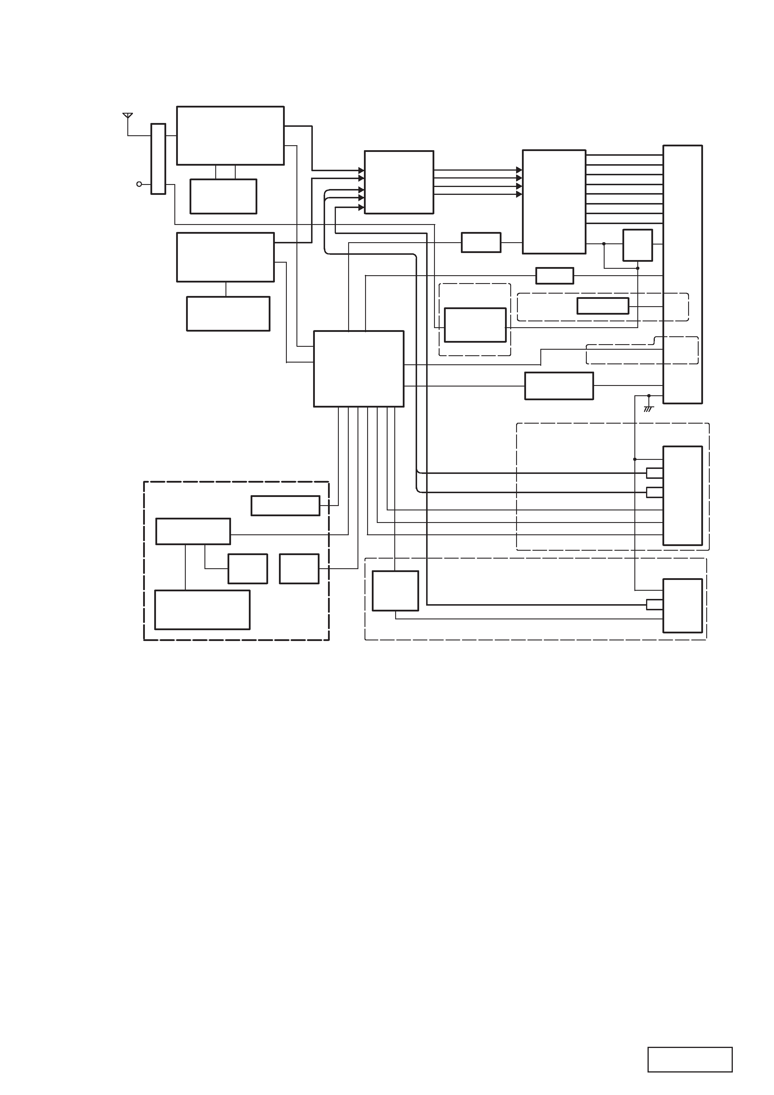
BLOCK DIAGRAM
AM/FM-TUNER
BL101
TUN
CD
A/C-R
A/C-L
E-VOL
IC302
POWER
IC402
BEEP
FIL
B/U
ILL
ACC-DET
Q415
TEL-ON
Q203
Q202
SUPPLY
POWER-
SYSTEM
CONTROLLER
IC201
VOL
KEY
LCD-DRIVER
IC700
LCD
LCD701
MAIN
GT13
-ANT
ANT
ANT
-ON
FR-L+
J401
(TH18)
J302
(A-12)
FR-L-
FR-R+
FR-R-
RR-L+
RR-L-
RR-R+
RR-R-
CD-L+
CD-L-
CD-R+
CD-R-
GND
REQ1
TXD
RXD
J301
(TH-08)
PN-2871F-B,R-A
PN-2871F-B,R-A
TEL(+)
TEL(-)
TEL-G
TEL-ON
B/U
ILL+
STR-A
STR-B
ACC
GND
SW-PWB
AM-NC
MECHANISM
CD-8V
Q410
CD-EJ
S715
CD
IC103
TEL
ILL-CONT
ILL-
PN-2871L-A,
L-G
Q406
PN-2871F,L,R
PP-2871T
L401
GLASS ANT
PN-2871F, L, R
PP-2871H-B, H-C, N-A, T