Service Manual
NISSAN MOTOR Genuine
6-disc CD/MP3/WMA Autochanger
AM/FM Radio Stereo
Model
Published by Service Dept.
298-6297-00 Nov. 2005 X
Printed in P.R.C.
(Genuine No. 28185 CL70A)
Clarion Co., Ltd.
50 Kamitoda, Toda-shi, Saitama 335-8511 Japan
Service Dept.: 5-66 Azuma, Kitamoto-shi, Saitama 364-0007 Japan
Tel: +81-48-541-2335/2432 FAX: +81-48-541-2703
PN-2708N-A/B
-1-
SPECIFICATIONS
Tuner section
Tuning system:
PLL synthesizer
Receive frequency:
AM
530kHz to 1710kHz
FM
87.75MHz to 107.9MHz
Intermediate frequency:
AM
450+3/-3kHz
FM
10.7+0.3/-0.3MHz
Quieting sensitivity:
AM
Less than 38dBu
FM
Less than 15dBu
Separation:
FM
22+5/-7dB(1kHz)
S/N ratio:
AM
More than 45dB
FM
More than 50dB
Auto stop sensitivity(DX): AM
42+6/-6dBu(600kHz)
39+6/-6dBu
(1000kHz, 1400kHz)
FM
32+6/-6dBu
CD changer section
Separation:
More than 60dB(20kHz LPF)
S/N ratio:
More than 74dB
Distortion:
Less than 0.1%(20kHz LPF)
AUX(CD) section
Separation:
More than 52dB(1kHz, 3.0V input)
S/N ratio:
More than 80dB(1kHz, 3.0V input)
CMRR:
More than 40dB(1kHz, 3.0V input)
General section
Load impedance:
300 ohm/4ch
Power output:
6V x 4
Power supply voltage:
DC 14.4V
Back up current:
Less than 0.5mA(at 13.2V)
Dimensions(mm):
180(W) x 106.4(H) x 167(D)
MP3/WMA operations:
MP3; Sampling rate 11.025kHz-48kHz
Bit rate: 8kbps-320kbps/VBR
WMA; Bit rate; 48kbps-192kbps/VBR
Logical format(File system);
ISO9660 level 1, 2 or JOLIET or Romeo
Weight:
2.75kg
PN-2708N-A/B
NOTE
* There are two models with a different production place.
China production:
PN-2708N-A
Philippines production: PN-2708N-B
All the same parts are used and assemble these models.
* This product includes technology owned by Microsoft Corporation
and cannot be used or distributed without a license from MSLGP.
* We cannot supply PWB with component parts in principle. When
a circuit on PWB has failure, please repair it by component parts
base. Parts which are not mentioned in service manual are not
supplied.
* Specification and design are subject to change without notice for
further improvement.
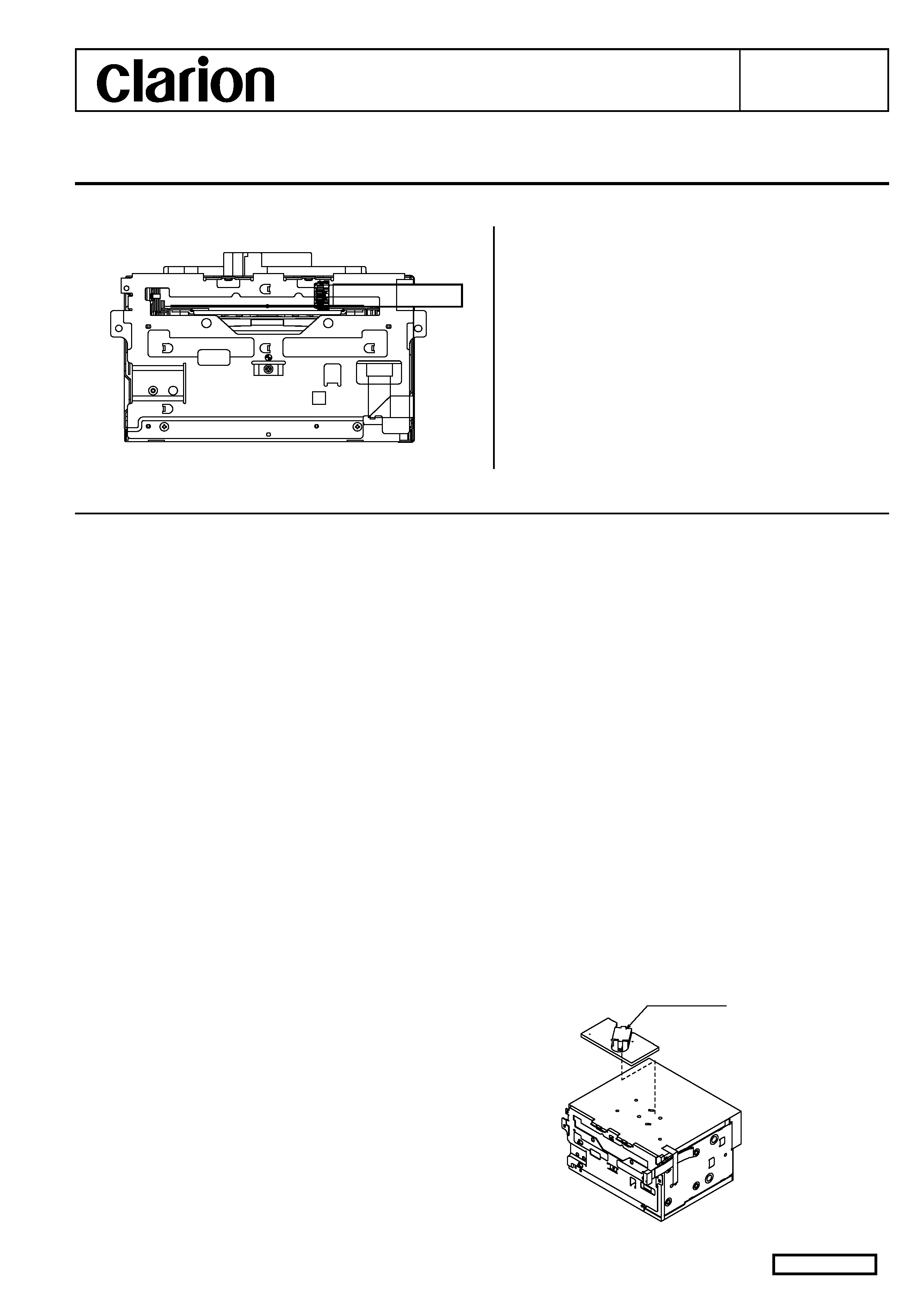
* In case that the main unit is transported for repair, the lock pin
(966-0653-21) must be set to fix the mechanism assy.
LOCK PIN
966-0653-21
-2-
COMPONENTS
PN-2708N-A/B
Main unit
-----------
1
9. Cautions in handling the optical pickup
The laser diode of the optical pickup can be damaged by electr-
ostatic charge caused by your clothes and body. Make sure to
avoid electrostatic charges on your clothes or body, or discharge
static electricity before handling the optical pickup.
9-1. Laser diode
The laser diode terminals are shorted for transportation in order
to prevent electrostatic damage. After replacement, open the
shorted circuit.
When removing the pickup from the mechanism, short the ter-
minals by soldering them to prevent this damage.
9-2. Actuator
The actuator has a powerful magnetic circuit. If a magnetic
material is put close to it. Its characteristics will change.
Ensure that not foreign substances enter through the ventilati-
on slots in the cover.
9-3. Cleaning the lens
Dust on the optical lens affects performance.
To clean the lens, apply a small amount of isopropyl alcohol to
lens paper and wipe the lens gently.
PN-2708N-A/B
To engineers in charge of repair or inspe-
ction of our products.
Before repair or inspection, make sure to follow the in-
structions so that customers and Engineers in charge
of repair or inspection can avoid suffering any risk or
injury.
1. Use specified parts.
The system uses parts with special safety features against fire
and voltage. Use only parts with equivalent characteristics when
replacing them.
The use of unspecified parts shall be regarded as remodeling for
which we shall not be liable. The onus of product liability (PL) sh-
all not be our responsibility in cases where an accident or failure
is as a result of unspecified parts being used.
2. Place the parts and wiring back in their original positions after re-
placement or re-wiring.
For proper circuit construction, use of insulation tubes, bonding,
gaps to PWB, etc, is involved. The wiring connection and routing
to the PWB are specially planned using clamps to keep away
from heated and high voltage parts. Ensure that they are placed
back in their original positions after repair or inspection.
If extended damage is caused due to negligence during repair,
the legal responsibility shall be with the repairing company.
3. Check for safety after repair.
Check that the screws, parts and wires are put back securely in
their original position after repair. Ensure for safety reasons there
is no possibility of secondary ploblems around the repaired spots.
If extended damage is caused due to negligence of repair, the
legal responsibility shall be with the repairing company.
CAUTION
Use of controls, adjustments, or performance of procedures other
than those specified herein, may result in hazardous radiation ex-
posure.
The compact disc player should not be adjusted or repaired by an-
yone except properly qualified service personnel.
4. Caution in removal and making wiring connection to the parts for
the automobile.
Disconnect the battery terminal after turning the ignition key off.
If wrong wiring connections are made with the battery connected,
a short circuit and/or fire may occur.
If extensive damage is caused due to negligence of repair, the
legal responsibility shall be with the repairing company.
5. Cautions regarding chips.
Do not reuse removed chips even when no abnormality is obser-
ved in their appearance. Always replace them with new ones.
(The chip parts include resistors, capacitors, diodes, transistors,
etc). The negative pole of tantalum capacitors is highly suscepti-
ble to heat, so use special care when replacing them and check
the operation afterwards.
6. Cautions in handling flexible PWB
Before working with a soldering iron, make sure that the iron tip
temperature is around 270 C. Take care not to apply the iron tip
repeatedly(more than three times) to the same patterns. Also ta-
ke care not to apply the tip with force.
7. Turn the unit OFF during disassembly and parts replacement.
Recheck all work before you apply power to the unit.
8. Cautions in checking that the optical pickup lights up.
The laser is focused on the disc reflection surface through the
lens of the optical pickup. When checking that the laser optical
diode lights up, keep your eyes more than 30cms away from the
lens. Prolonged viewing of the laser within 30cms may damage
your eyesight.
Top view of the unit
Guide label
T H I S
P R O D U C T I O N
C O M P L I E S
W I T H
D H H S
R U L E S
2 1
C F R
S U B C H A P T E R
J
A P P L I C A B L E
A T
D A T E
O F
M A N U F A C T U R E .
I N T E R F E R E N C E
T H A T
M A Y
C A U S E
U N D E S I R E D
O P E R A T I O N .
T H I S
D E V I C E
C O M P L I E S
W I T H
P A R T
1 5
O F
T H E
F C C
R U L E S .
O P E R A T I O N
I S
S U B J E C T
T O
T H E
F O L L O W I N G
T W O
C O N D I T I O N S : ( 1 )
T H I S
D E V I C E
M A Y
N O T
C A U S E
H A R M F U L
I N T E R F E R E N C E , A N D ( 2 )
T H I S
D E V I C E
M U S T
A C C E P T
A N Y
I N T E R F E R E N C E
R E C E I V E D , I N C L U D I N G
Th i s p r o d u c t
i n c l u de s t e c h n o l og y own ed b y M i c r o s o f t Co r p o r a t i o n a nd
c a nn o t b e u s e d o r d i s t r i bu t ed w i t h o u t a l i c e n s e f r om MSLGP .

-3-
PN-2708N-A/B
EXPLANATION OF IC
052-3177-40
M30624MGA-EM6GP
System Controller
1.Terminal Description
pin 1
: 1CD/6CD
: IN : The initial setting terminal. High = 1CD, Low=
6CD.
pin 2
: TAPE SEL
: IN : The initial setting terminal. High = without tape.
pin 3
: SCV SEL
: IN : The initial setting terminal. Low = without SCV.
pin 4
: NU
: - : Not in use.
pin 5
: ES RETURN
: IN : The flexible PWB connection OK flag input.
pin 6
: BYTE
: IN : The data length selection(8bit/16bit).
pin 7
: CN VSS
: IN : Connect to VSS.
pin 8
: TEST
: - : For the Test.
pin 9
: ILL ON
: IN : Illumination ON signal input.
pin 10 : RESET
: IN : Reset signal input.
pin 11 : X OUT
: O : Crystal connection.
pin 12 : GND
: - : Ground.
pin 13 : X IN
: IN : Crystal connection.
pin 14 : VDD
: - : Positive supply voltage.
pin 15 : NU
: - : Not in use.
pin 16 : BU DET
: IN : Backup detection signal input.
pin 17 : ACC IN
: IN : ACC ON flag input.
pin 18 : TEL
: IN : The telephone interrupt pulse input.
pin 19 : SBSY
: IN : Sub code block synchronous signal detection
input.
pin 20 : AMP ON
: O : Audio power amplifier ON signal output.
pin 21 : SYS ON
: O : System ON signal output.
pin 22 : NU
: - : Not in use.
pin 23 : REAR MUTE
: O : The audio mute signal output for the rear cha-
nnels.
pin 24 : NU
: - : Not in use.
pin 25 : FRONT MUTE : O : The audio mute signal output for the front cha-
nnels.
pin 26 : 6-CD REQ
: IN : The request signal input from the 6CD-
Changer.
pin 27 : 6-CD RX
: IN : The serial data input for 6CD-Changer.
pin 28 : 6-CD TX
: O : The serial data output for 6CD-Changer.
: 1-CD ON
: O : Power supply ON signal output for 1-CD.
pin 29 : NDS FLASH TX : O : NDS serial data output for external A/C.
pin 30 : NDS FLASH RX : O : NDS serial data input for external A/C.
pin 31 : FLASH CLK
: O : Clock pulse output for flash memory.
pin 32 : NU
: - : Not in use.
pin 33 : DCU TX
: O : The serial data output to DCU.
pin 34 : DCU RX
: IN : The serial data input from DCU.
pin 35 : NDS CNT
: O : Low = A/C 1, High = A/C 2.
pin 36 : NDS REQ 2
: IN : NDS request signal input.
pin 37 : NDS REQ 1
: IN : NDS request signal input.
pin 38 : SOURCE CHG : O : The signal source change signal output.
pin 39 : FLASH EPM
: O : FLASH EPM.
pin 40 : VOL EEP-R DO : O : Serial data output for Volume IC or EEP-ROM.
pin 41 : VOL EEP-R CK : O : Clock pulse output for Volume IC or EEP-ROM.
pin 42 : VOL CE
: O : The chip enable signal output to the volume IC.
pin 43 : EEPROM CE
: O : The chip enable signal output to EEP-ROM.
pin 44 : FLASH CE
: IN : Chip enable signal input for flash memory.
pin 45 : EEPROM DI
: IN : Serial data input from the EEP-ROM.
pin 46 : NU
: - : Not in use.
pin 47 : AUX ON
: IN : AUX(DVD) ON signal input.
pin 48 : COMBI ON
: O : Combi(DVD) ON signal output.
pin 49 : BUC 0
:I/O : CD IC Data input / output.
pin 50 : BUC 1
:I/O : CD IC Data input / output.
pin 51 : BUC 2
:I/O : CD IC Data input / output.
pin 52 : BUC 3
:I/O : CD IC Data input / output.
pin 53 : BUC CLOCK
: O : CD IC clock pulse output.
pin 54 : CCE
: O : The chip enable signal output.
pin 55 : CD RESET
: O : The reset pulse output to the CD IC.
pin 56 : S STOP
: IN : Inside limit signal input from the CD mecha-
nism.
pin 57 : CHU SW
: IN : CD disc chucking signal input.
pin 58 : TR A
: IN : Photo sensor signal input from the CD mec-
hanism.
pin 59 : TR B
: IN : Photo sensor signal input from the CD mec-
hanism.
pin 60 : VDD
: - : Positive supply voltage.
pin 61 : LD CONT
:I/O : Loading motor control signal output.
pin 62 : GND
: - : Ground.
pin 63 : PLL CE
: O : The chip enable signal output to the PLL IC.
pin 64 : PLL CLK
: O : The clock pulse output to the PLL IC.
pin 65 : PLL DO
: O : Serial data output to the PLL IC.
pin 66 : PLL DI
: IN : Serial data input from the PLL IC.
pin 67 : ST/TWEET
: I/O : Outputs "L" at AM 900kHz receiving. Inputs
"L" at FM stereo receiving.
pin 68 : AMP MUTE
: O : Muting signal output to the Audio Power Amplifier.
pin 69 : MECH MUTE
: O : Muting signal output to the Tape mechanism.
pin 70 : RDS DI
: IN : RDS data input.
pin 71 : RDS CLK
: IN : RDS clock pulse input.
pin 72 : NU
: - : Not in use.
pin 73 : TAPE IN
: IN : The tape in signal input.
pin 74 : MODE BIT 1
: IN : The mode bit input from the tape mechanism.
pin 75 : MODE BIT 2
: IN : The mode bit input from the tape mechanism.
pin 76 : MODE BIT 3
: IN : The mode bit input from the tape mechanism.
pin 77 : REEL PULSE
: IN : Reel pulse input from the tape mechanism.
pin 78 : APC SENSE
: O : APC gain control signal output.
pin 79 : APC DET I
: IN : APC detected signal input.
pin 80 : PWR MTR 1
: O : Power motor control signal output.
pin 81 : PWR MTR 2
: O : Power motor control signal output.
pin 82 : MAIN MTR
: O : Main motor control signal output.
pin 83 : NR
: O : Noise reduction control.
pin 84 : FWD/REV
: O : Forward/Reverse selection.
pin 85 : LD MUTE
: O : Muting signal output to the CD mechanism.
pin 86 : CD CONNECT : IN : CD connection check signal input.
pin 87 : 6-CD LOAD
: IN : The loading control signal input for 6CD-
Changer.
pin 88 : TAPE EJECT
: IN : Tape eject signal input.
pin 89 : 6-CD EJECT
: IN : The eject signal input for 6CD-Changer.
pin 90 : NAVI MUTE
: O : Muting signal output to suppress the noise
without Navigation sound interrupting.
pin 91 : TF SELECT
: IN : High = TF.
pin 92 : IX6 SELECT
: IN : Low = IX6-MP3, High = IX6.
pin 93 : FAN ON
: O : High = FAN ON.
pin 94 : A VSS
: - : Analog ground.
pin 95 : CD-MP3 ON
: - : Power supply control. High = ON.
pin 96 : Vref
: - : Reference voltage.
pin 97 : A VDD
: - : Positive supply voltage for the internal analog
section. Low = with RDS
pin 98 : RDS SEL
: IN : The initial setting terminal.
High = without RDS.
pin 99 : USA/EXP
: O : High = USA, Low = EXP
pin100 : BOSE AMP SEL : IN : The initial setting terminal.
High = BOSE amplifier.
052-5062-04
MBM29DL800BA-90PFTN
8 M bit Flash Memory
1.Terminal Description
pin 1 : Address 15
: IN : Address signal input.
pin 2 : Address 14
: IN : Address signal input.
pin 3 : Address 13
: IN : Address signal input.
pin 4 : Address 12
: IN : Address signal input.
pin 5 : Address 11
: IN : Address signal input.
pin 6 : Address 10
: IN : Address signal input.
pin 7 : Address 9
: IN : Address signal input.
pin 8 : Address 8
: IN : Address signal input.
pin 9 : NU
: - : Not in use.
pin 10 : NU
: - : Not in use.
pin 11 : WE
: IN : Write enable signal input.
pin 12 : RESET
: IN : Reset signal input.
pin 13 : NU
: - : Not in use.
pin 14 : NU
: - : Not in use.
pin 15 : Ready/Busy
: O : Ready/Busy flag output, High = Ready.
pin 16 : Address 18
: IN : Address signal input.
pin 17 : Address 17
: IN : Address signal input.
pin 18 : Address 7
: IN : Address signal input.
pin 19 : Address 6
: IN : Address signal input.
pin 20 : Address 5
: IN : Address signal input.
pin 21 : Address 4
: IN : Address signal input.
pin 22 : Address 3
: IN : Address signal input.
pin 23 : Address 2
: IN : Address signal input.
pin 24 : Address 1
: IN : Address signal input.
pin 25 : Address 0
: IN : Address signal input.
pin 26 : CE
: IN : Chip enable signal input.
pin 27 : VSS
: - : Negative supply voltage.
pin 28 : OE
: IN : Output enable signal input.
pin 29 : DQ 0
: I/O: The data input / output.
pin 30 : DQ 8
: I/O: The data input / output.
pin 31 : DQ 1
: I/O: The data input / output.
-4-
PN-2708N-A/B
pin 32 : DQ 9
: I/O: The data input / output.
pin 33 : DQ 2
: I/O: The data input / output.
pin 34 : DQ 10
: I/O: The data input / output.
pin 35 : DQ 3
: I/O: The data input / output.
pin 36 : DQ 11
I/O: The data input / output.
pin 37 : VCC
: - : Positive supply voltage.
pin 38 : DQ 4
: I/O: The data input / output.
pin 39 : DQ 12
: I/O: The data input / output.
pin 40 : DQ 5
: I/O: The data input / output.
pin 41 : DQ 13
: I/O: The data input / output.
pin 42 : DQ 6
: I/O: The data input / output.
pin 43 : DQ14
: I/O: The data input / output.
pin 44 : DQ 7
: I/O: The data input / output.
pin 45 : DQ 15/A-1
: I/O: The data input/output,TheAddress signal input.
pin 46 : VSS
: - : Negative supply voltage.
pin 47 : BYTE
: IN : The data length selection(8bit/16bit).
pin 48 : Address 16
: IN : Address signal input.
ADJUSTMENT
FM noise
convergence
1. Input the 98.1MHz/55dBu(1kHz,30% MOD) signal. (Volume max.=0dB)
2. Adjust the outputs to -22+3/-3dB by VR102 when the SG output is set -20dBu.
SSG
Milli-volt meter
Item
Procedure
Measuring
instrument
FM
Diversity
1. Use only Main side of the diver antenna receptacle.
2. SSG input the 98.1MHz(1kHz, 30% MOD) signal of Main side.
3. Turn VR101 until minimum level.
4. Connect a digital tester to TP101(DIV-TP).
5. Adjust VR101 to the point where the voltage starts just to increase(100mV approx).
SSG
Digital tester
SERVO
DRIVER
BL101
AM/FM
TUNER
LPF
IC104
LC72191
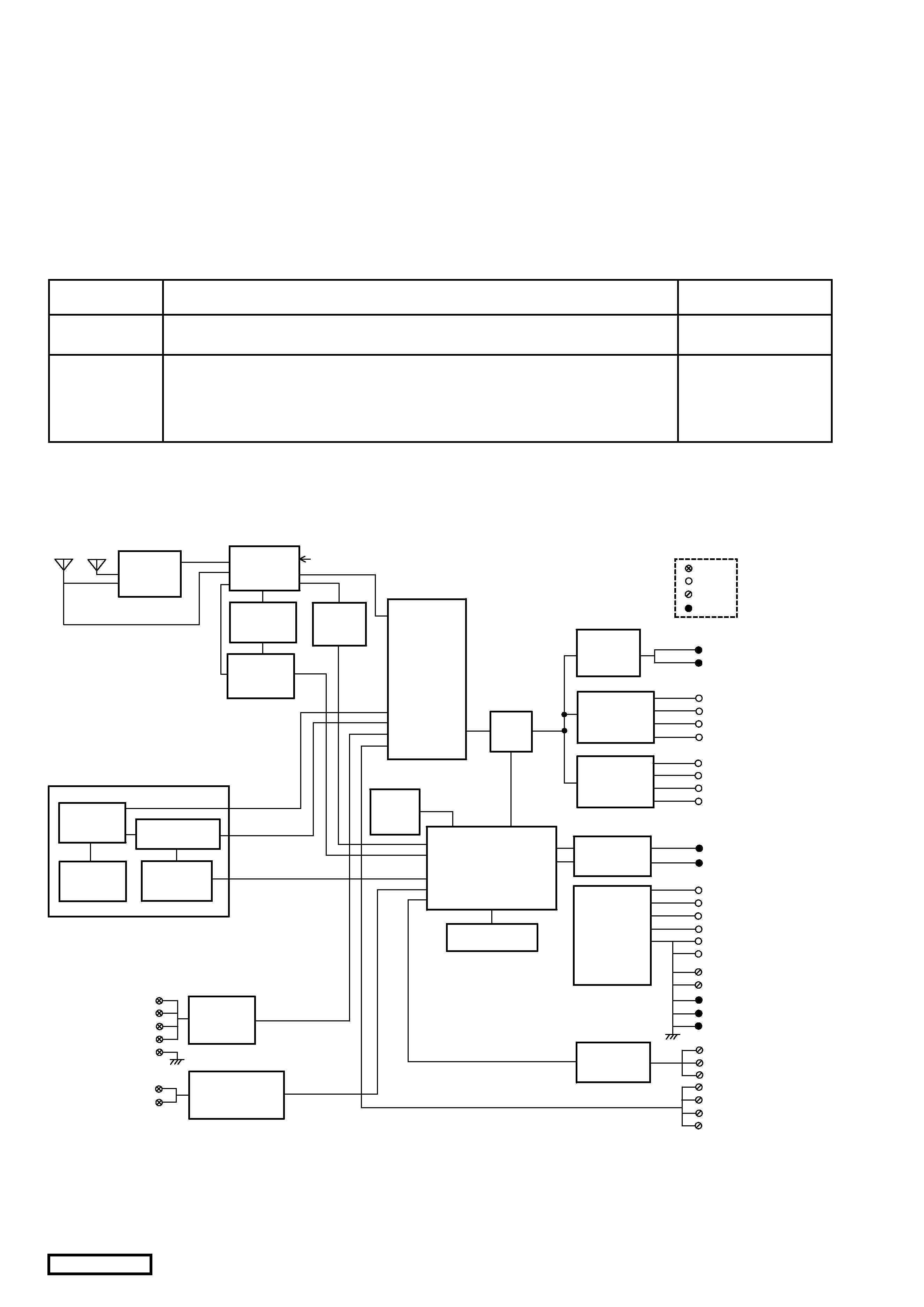
JM
CD CHANGER MECHANISM
RF & CDIC
DSP
CPU
IC405
NJM4558V
NAVI AMP
IC401
LC75412WS
ELECTRONIC
VOLUME
MUTE
IC203
S-80933
ANMP
IC202
M30624MGA-EM6GP
POWER
SUPPLY
PANEL SW
A/C
INTERFACE
J301
J602
J603
CONNECTOR
6. NAVI INPUT (+)
5. NAVI INPUT (-)
A. FR SP L-CH (+)
E. FR SP L-CH (-)
B. FR SP R-CH (+)
F. FR SP R-CH (-)
O. RR SP L-CH (+)
N. RR SP L-CH (-)
L. RR SP R-CH (+)
P. RR SP R-CH (-)
G. ANT SIGNAL
H. B/U
D. ACC
J. GND
M. GND
7. EARTH
8. SHEILD-EARTH
9. DATA GND
15. GND
1. CD L-CH INPUT (+)
5. CD L-CH INPUT (-)
2. CD R-CH INPUT (+)
6. CD R-CH INPUT (-)
10. REQ (CD-COMBI)
11. RXD (CD-COMBI)
3. TXD (COMBI-CD)
IC103
RDS
SAA6581
IC403,406
NJM4556AL
BUFFER AMP
IC404,407
NJM4556AL
BUFFER AMP
K. AMP ON
IC101
LA1061M
DIVER-IC
880-1921V
MAIN SUB
AUD-DCU
INTERFACE
7. TX (AUD-DCU)
8. RX (DCU-AUD)
16. GND
IC402
NJM4565V
AUX AMP
1. L-CH INPUT (+)
3. L-CH INPUT (-)
6. R-CH INPUT (-)
7. R-CH INPUT (+)
2. AUDIO-ON
4. DVD-ON
8. GND
AUX / COMBI-ON
INTERFACE
Q406,407
J401
BLOCK DIAGRAM
Main section
-5-
CD changer module section
PN-2708N-A/B
A
U
D
IO
L
,R
3m
A
22
m
A
5m
A
3m
A
11
1m
A
60
m
A
40
m
A
21
5m
A
R
F &
C
D
IC
T
C
94
A
15
F
IC
2
D
S
P
T
M
S
32
0D
A
14
0
IC
9
M
IC
O
M
M
30
62
1
IC
3
E
E
P
R
O
M
(2
K
)
B
R
93
L5
6R
F
V
M
IC
4
V
D
D
R
E
F
3.
3V
Q
5
P
-O
N
1
D
S
P
P
W
B
(B
3)
10
M
H
z
S
E
R
V
O
D
R
IV
E
R
B
D
79
61
F
M
IC
3
R
E
S
E
T
B
D
52
27
G
IC
2
M
O
T
O
R
D
R
IV
E
R
IC
1
IC
6
S
Y
S
-A
C
C
T
X
,R
X
(S
D
A
,S
C
L)
A
C
C
3.
3V
B
A
03
3S
F
P
IC
6
D
R
IV
E
R
P
W
B
(B
6)
P
IC
K
-U
P
S
P
IN
D
LE
M
O
T
O
R
S
LE
D
M
O
T
O
R
M
3
M
2
S
2
M
O
D
E
M
O
T
O
R
V
M
O
T
O
R
LO
A
D
IN
G
M
O
T
O
R
M
1
V
-
IN
T
S
W
S
1
M
E
C
H
S
E
N
S
O
R
P
W
B
(B
4)
D
IS
C
S
E
N
S
O
R
M
O
D
E
-
IN
T
S
W
S
1
IC
5
M
O
D
E
S
E
N
S
O
R
P
T
1
V
S
E
N
S
O
R
LE
D
P
W
B
(L
&
R
)(
B
8
&
B
9)
LE
D
P
O
N
1
S
H
U
T
-S
W
B
/U
-D
E
T
25
m
A
P
LA
Y
25
0m
A
M
E
C
H
M
O
V
E
12
00
m
A
(M
A
X
)
B
/U
-5
V
V
D
D
3.
3V
N
JU
72
22
U
33
IC
5
S
D
-R
A
M
(6
4M
)
K
4S
64
16
32
F
IC
7
D
E
C
O
D
E
S
N
74
LV
13
9
IC
4
F
LA
S
H
R
O
M
M
B
M
29
D
L8
00
B
A
IC
5
C
LK
IN
16
.9
2M
H
z
A
U
D
IO
L-
C
H
,R
-C
H
B
U
S
0
B
U
S
1
B
U
S
2
B
U
S
3
B
U
C
K
/C
C
E
S
IG
N
A
L
(I
N
T
)
(I
N
T
)
(I
N
T
)
D
E
C
O
D
E
/
LA
T
C
H
74
LV
13
9
/7
4L
V
74
IC
6
IC
8
D
A
C
LR
C
K
I/O
A
U
D
IO
D
A
T
A
(6
)
B
U
S
(6
)
B
C
LK
I/O
D
A
T
A
I/O
S
E
N
S
O
R
9V
Q
8
,Q
9
V-BU
S
T
X
A
-M
U
T
E
(T
O
S
E
T
U
-C
O
M
)
LE
D
-S
W
(P
O
N
3)
B
U
S
B
U
F
F
E
R
F
E
T
Q
4
,Q
6
,Q
53
M
E
C
H
M
O
D
U
LE
C
O
N
N
E
C
T
O
R
(T
o
M
ai
n
U
ni
t)
J
3
D
S
P
1.
6V
T
P
S
76
31
6D
B
IC
10
33
m
A
25
m
A
42
6m
A
D
R
IV
E
U
N
IT
LI
M
IT
S
W
P
-O
N
2
D
R
M
U
T
E
LM
T
-S
W
R
E
S
E
T
S
E
R
IA
L
S
E
R
IA
L
S
E
R
IA
L
N
-B
U
S
(I
2C
)
C
D
P
W
B
(B
2)
C
C
S
C
S
R
Q
C
M
S
I
C
M
S
O
C
S
C
K
C
C
S
C
S
R
Q
C
M
S
I
C
M
S
O
C
S
C
K
V-BU
S
S
F
S
Y
S
B
S
Y
IP
F M
B
O
V
R
E
S
E
T
E
M
P
H
O
W
U
P
W
U
P
A
-
M
U
T
E
R
E
S
E
T
M
O
D
E
61
m
A
50
m
A
16
.9
2M
H
z
JT
A
G
IE
E
E
11
49
.1
E
M
U
0
E
M
U
1
TC
K
TC
K
_R
E
T
TD
O
TD
I
TM
S
/T
R
S
T
3.
3V
G
N
D
JT
A
G
(1
5P
IN
)
E
M
P
H
I
17
0m
A
45
m
A
33
m
A
42
6m
A
M
E
C
H
M
O
V
E
12
00
m
A
(M
A
X
)
P
LA
Y
25
0m
A
R
E
Q
20
uA
2.
6u
A
IC
11
IN
V
R
X
3.
3V
2S
B
11
88
Q
2
11
1m
A
SYSP
S
Y
S
C
LK
IC
12
IN
V
IC
13
B
U
F
F
IN
T
S
E
R
IA
L
S
E
R
IA
L
S
E
R
IA
L
U
A
R
T