PN-2302M/N
- 1 -
Published by Service Dept.
Printed in Japan
Clarion Co., Ltd.
Export Division - 22-3, Shibuya 2-chome, Shibuyaku, Tokyo, 150-8335 Japan Tel: 03-3400-1121
Service Dept.- 50 kamitoda,Toda-shi,Saitama,335-8511 Japan Tel: 048-443-1111 FAX:048-433-6996
298-5827-00 Feb.2000 B
Service Manual
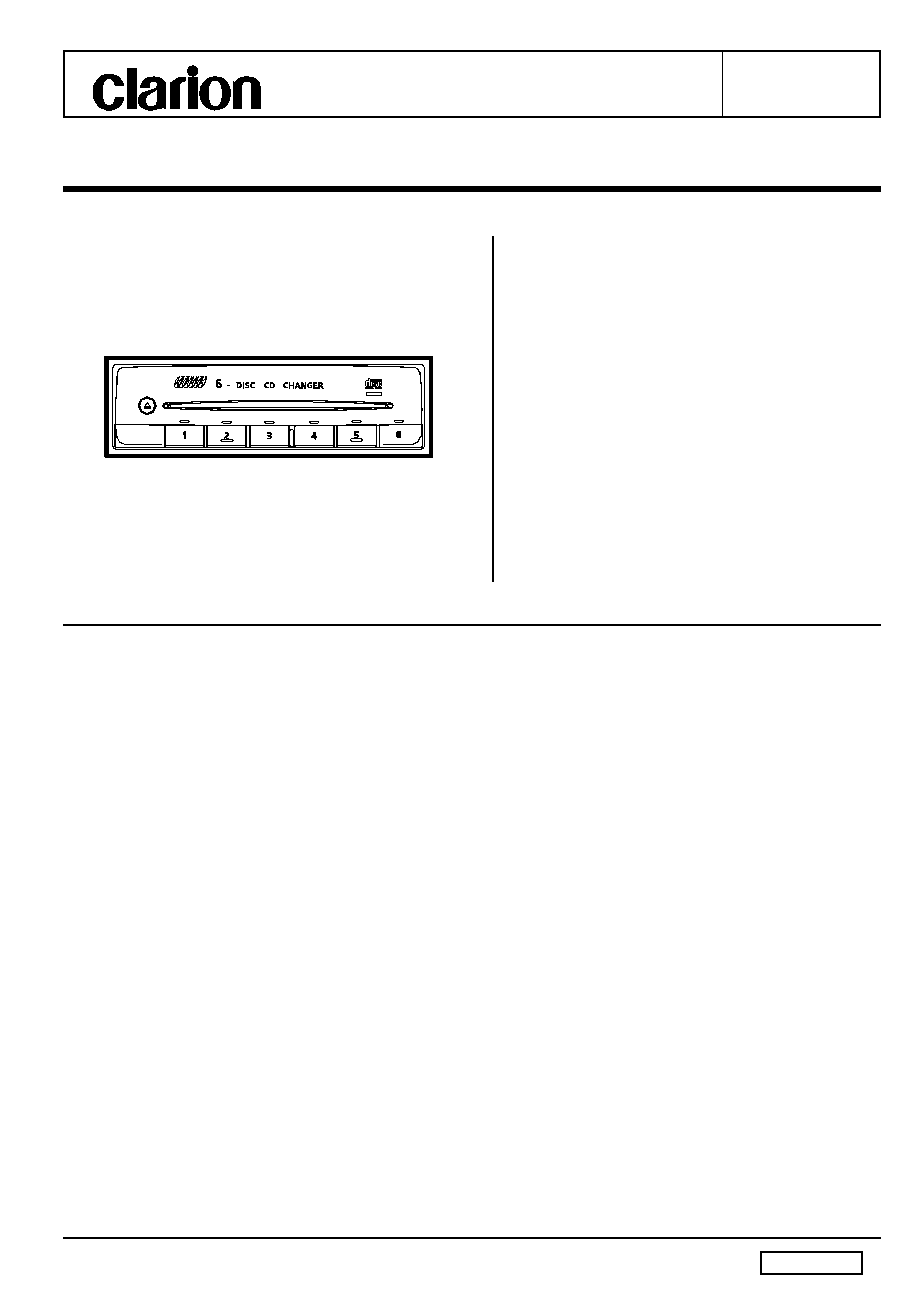
NISSAN Automobile Genuine
6-Disc CD Changer Deck
PN-2302M-C
(Genuine No.28184 4M500/ID No.CE008)
PN-2302M-F
(Genuine No.B8184-89961/ID No.CE008)
PN-2302N-A
(Genuine No.28184 3W400/ID No.CE018)
·¡
SPECIFICATIONS
Output level:
3.0V·}2dB(at 1kHz,0dB DISC)
Frequency characteristics:
17 Hz to 20kHz (·}2dB)
Channel separation:
More than 70dB
(at 1kHz,0dB DISC,Filter:20kHz LPF)
Distortion:
Less than 0.02%
(at 1kHz,0dB DISC,Filter:20kHz LPF)
Power supply voltage: DC13.2V(10.8 to 15.6V)
Negative ground
Current consumption: 0.6A (during playing)
Dimensions(mm):
184(W)·~56(H)·~170(D)
Weight:
approximately 1.6kg
·¦
Specification and design are subject to change without
notice for further improvement.
Model
Model
Model
·¡
COMPONENTS
PN-2302M-C
PN-2302N-A
Main unit
·|·|·|·|·|
1
PN-2302M-F
Main unit
·|·|·|·|·|
1
Parts bag
·|·|·|·|·|
Machine screw(M5·~8)
714-5008-41
4
·¡
NOTES
·E
Model PN-2302M has an anti-theft system.The special
equipment is necessary to operate the unit without con-
necting the vehicle.
·E
We can not supply PWB with component parts in prin-
ciple. When a circuit on PWB has failure, please repair
it by component parts base. Parts which are not men-
tioned in service manual are not supplied.
·¡
To engineers in charge of repair or
inspection of our products.
Before repair or inspection, make sure to follow
the instructions so that customers and Engineers
in charge of repair or inspection can avoid suf-
fering any risk or injury.
1. Use specified parts.
The system uses parts with special safety features against
fire and voltage. Use only parts with equivalent charac-
teristics when replacing them.
The use of unspecified parts shall be regarded as re-
modeling for which we shall not be liable. The onus of
product liability (PL) shall not be our responsibility in cases
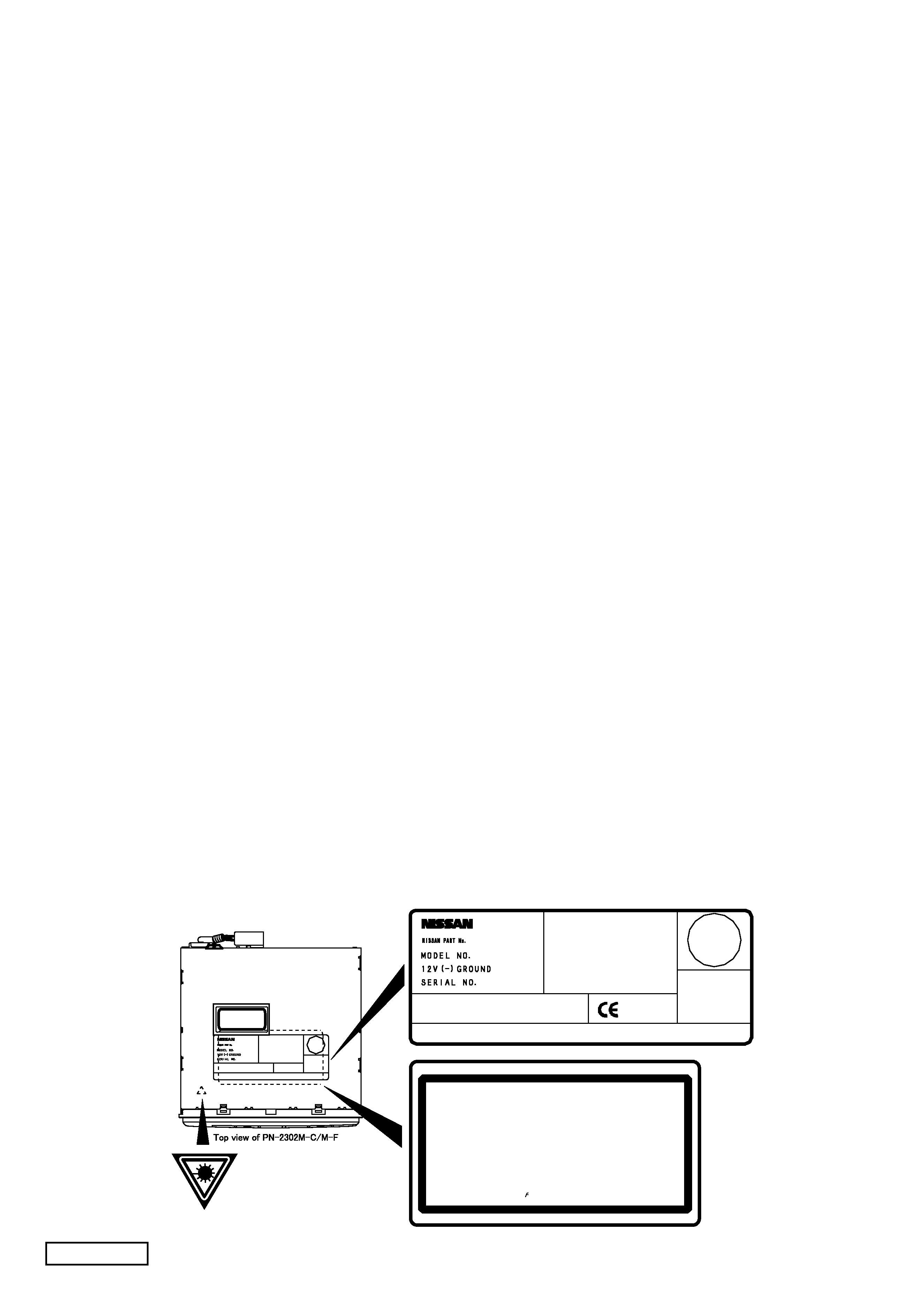
INVISIBLE LASER RADIATION WHEN OPEN AND
INTERLOCKS DEFEATED. AVOIDE EXPOSURE TO BEAM.
CAUTION·|
CLASS 1 LASER PRODUCT
THIS DEVICE COMPLIES WITH
PART 15 OF THE FCC RULES.
OPERATION IS SUBJECT TO
THE FOLLOWING TWO CONDITIONS
: (1) THIS DEVICE MAY NOT
CAUSE HARMFUL INTERFERENCE.
AND (2) THIS DEVICE MUST
ACCEPT ANY INTERFERENCE
RECEIVED INCLUDING
INTERFERENCE THAT MAY CAUSE
UNDESIRED OPERATION.
MANUFACTURED DATE:
Clarion Co.,Lt d
50 KAMITODA, TODA SHI, SAITAMA KEN, JAPAN
UNSICHTBARE LASERSTRAHLUNG TRITT AUS.
WENN DECKEL GEOFFENET UND WENN
SICHERHEITSVERRIEGELUNG UBERBRUCKT IST.
NICHT DEM STRAHL AUSSETAZEN!
VORSICHT!
ADVARSEL·|
VARNING·| OSYNLIG LASERSTRALNING NAR DENNA DEL
AR OPPNAD OCH SPARR AR URKOPPLAD.
STRALEN AR FARLIG.
USYNLIG LASERSTRALING VED ABNING, NAR
SIKKERHEDSAFBRYDERE ER UDE AF FUNKTION.
UNDGA UDS ETTELSE FOR STRALING.
·B
·B·B
·B·B
·B
·B·B
·B·B
·B·B
·B·B
·B
·B
·B
THIS PRODUCTION
COMPLIES WITH
DHHS RULES 21
CFR SUBCHAPTER
J APPLICABLE
AT DATE OF
MANUFACTURE.
MADE IN JAPAN
PART No.
PN-2302M/N
- 2 -
·¡
CAUTIONS
USE OF CONTROLS,OR ADJUSTMENTS,MAY RESULT
IN HAZARDOUS RADIATION EXPOSURE.
THE COMPACT DISC PLAYER SHOULD NOT BE AD-
JUSTED OR REPAIRED BY ANYONE EXCEPT PROP-
ERLY QUALIFIED SERVICE PERSONNEL.
where an accident or failure is as a result of unspecified
parts being used.
2. Place the parts and wiring back in their original positions
after replacement or re-wiring.
For proper circuit construction, use of insulation tubes,
bonding, gaps to PWB, etc, is involved. The wiring con-
nection and routing to the PWB are specially planned
using clamps to keep away from heated and high voltage
parts. Ensure that they are placed back in their original
positions after repair or inspection.
If extended damage is caused due to negligence during
repair, the legal responsibility shall be with the repairing
company.
3. Check for safety after repair.
Check that the screws, parts and wires are put back se-
curely in their original position after repair. Ensure for
safety reasons there is no possibility of secondary
ploblems around the repaired spots.
If extended damage is caused due to negligence of re-
pair, the legal responsibility shall be with the repairing
company.
4. Caution in removal and making wiring connection to the
parts for the automobile.
Disconnect the battery terminal after turning the ignition
key off. If wrong wiring connections are made with the
battery connected, a short circuit and/or fire may occur.
If extensive damage is caused due to negligence of re-
pair, the legal responsibility shall be with the repairing
company.
5. Cautions regarding chips.
Do not reuse removed chips even when no abnormality
is observed in their appearance. Always replace them
with new ones. (The chip parts include resistors, capaci-
tors, diodes, transistors, etc). The negative pole of tanta-
lum capacitors is highly susceptible to heat, so use spe-
cial care when replacing them and check the operation
afterwards.
6. Cautions in handling flexible PWB
Before working with a soldering iron, make sure that the
iron tip temperature is around 270·Z. Take care not to
apply the iron tip repeatedly(more than three times)to the
same patterns. Also take care not to apply the tip with
force.
7. Turn the unit OFF during disassembly and parts replace-
ment. Recheck all work before you apply power to the
unit.
8. Cautions in checking that the optical pickup lights up.
The laser is focused on the disc reflection surface through
the lens of the optical pickup. When checking that the
laser optical diode lights up, keep your eyes more than
30cms away from the lens. Prolonged viewing of the la-
ser within 30cms may damage your eyesight.
9. Cautions in handling the optical pickup
The laser diode of the optical pickup can be damaged by
electrostatic charge caused by your clothes and body.
Make sure to avoid electrostatic charges on your clothes
or body, or discharge static electricity before handling the
optical pickup.
9-1. Laser diode
The laser diode terminals are shorted for transpor-
tation in order to prevent electrostatic damage.
After replacement, open the shorted circuit. When
removing the pickup from the mechanism, short
the terminals by soldering them to prevent this
damage.
9-2. Actuator
The actuator has a powerful magnetic circuit. If a
magnetic material is put close to it. its characteris-
tics will change. Ensure that no foreign substances
enter through the ventilation slots in the cover.
9-3. Cleaning the lens
Dust on the optical lens affects performance. To
clean the lens, apply a small amount of isopropylalcohol
to lens paper and wipe the lens gently.
PN-2302M/N
- 3 -
FEATURES
EXPLANATION OF IC
PD78078GC-A13-8EU
052-5034-00 1-DIN 6-CD A/C Controller
1. Terminal Description
pin
1 : X Wr INH_
: IN : DRAM write inhibit signal input from
*SPMC. Negative logic.
pin
2 : S DTO
: IN : Serial status data input from *SPMC.
pin
3 : X S O EN_
: O : Serial status data output enable signal
output to *SPMC. Negative logic.
pin
4 : XLT_
: O : Latch pulse output to *SPMC. Negative
logic.
pin
5 : A VSS
: - : Ground for the internal ADC.
pin
6 : X RD EN_
: O : DRAM read enable signal output to
*SPMC. Negative logic.
pin
7 : X WR EN_
: O : DRAM write enable signal output to
*SPMC. Negative logic.
pin
8 : A Vref
: - : Not in use.
pin
9 : NDS RX D
: IN : NDS serial data input.
pin 10 : NDS TX D
: O : NDS serial data output.
pin 11 : NDS SRQ_
: O : NDS slave request pulse output. Nega-
tive logic.
pin 12 : VSS
: - : Ground.
pin 13 : SQSO
: IN : SUB-Q data input from CDX2548.
pin 14 : NU
: - : Not in use.
pin 15 : SQ CK
: O : Clock pulse output to read SUB-Q -
Data from CDX2548.
pin 16 : BEEP OUT
: O : Beep output 4.8kHz.
pin 17 : ILL_
: IN : Illumination ON signal input. Negative
logic.
pin 18 : Q TBC
: IN : Playback data time information input
from *SPMC.
pin 19 : NU
: - : Not in use.
pin 20 : Q R CK
: O : Playback data time information read
clock output to *SPMC.
pin 21 : LOAD CW
: O : Disc loading / Drive unit transfer motor
control.
pin 22 : LOAD CCW
: O : Disc loading / Drive unit transfer motor
control.
pin 23 : Up/Dw CW
: O : Mode plate transfer / Stage up down
motor control.
pin 24 : Up/Dw CCW
: O : Mode plate transfer / Stage up down
motor control.
pin 25 : SHAVE CW
: O : Chuck and holder transfer motor con-
trol.
pin 26 : SHAVE CCW
: O : Chuck and holder transfer motor con-
trol.
pin 27 : P ON 1
: O : "H"= Mechanism ON.
pin 28 : P ON 2
: O : "H"= CD play.
pin 29 : NU
: IN : Connect to VDD.
pin 30 : DISC 1 KEY_
: IN : Disc 1 Key switch input. Negative log-
ic.
pin 31 : DISC 2 KEY_
: IN : Disc 2 Key switch input. Negative log-
ic.
pin 32 : DISC 3 KEY_
: IN : Disc 3 Key switch input. Negative log-
ic.
pin 33 : DISC 4 KEY_
: IN : Disc 4 Key switch input. Negative log-
ic.
pin 34 : DISC 5 KEY_
: IN : Disc 5 Key switch input. Negative log-
ic.
pin 35 : DISC 6 KEY_
: IN : Disc 6 Key switch input. Negative log-
ic.
pin 36 : EJECT KEY _ : IN : Eject key switch input. Negative logic.
pin 37 : S CLR_
: O : Clear signal output to Dual color LED
control.
pin 38 : S STB
: O : Strobe pulse output to Dual color LED
control.
pin 39 : S CLK
: O : Clock pulse output to Dual color LED
control.
pin 40 : S DATA
: O : Serial data output to Dual color LED
control.
pin 41 : LIM SW
: IN : Disc innermost track detection signal
input.
pin 42 : ILL SEL_
: IN : "H"= Without illumination control.
pin 43 : VSS
: - : Ground.
pin 44 : DIM ON
: O : "H"= Dimmer ON.
pin 45 : MUTE
: O : "H"= Mute ON.
pin 46 : PT 1_
: IN : Mode plate position count photo cou-
pler input. Negative logic.
pin 47 : SW 3_
: IN : Shut door close detection signal input.
Negative logic.
pin 48 : SW 1_
: IN : Datum point detection signal input for
the mode plate. Negative logic.
pin 49 : SW 2_
: IN : Eject arm end detection signal input.
Negative logic.
pin 50 : SW 4_
: IN : Datum point detection signal input for
the wedge. Negative logic.
(
((

PN-2302M/N
- 4 -
PD78078GC-A14-8EU
052-5034-10 1-DIN 6-CD A/C Controller
1. Terminal Description
pin
1 : X Wr INH_
: IN : DRAM write inhibit signal input from
*SPMC. Negative logic.
pin
2 : S DTO
: IN : Serial status data input from *SPMC.
pin
3 : X S O EN_
: O : Serial status data output enable signal
output to *SPMC. Negative logic.
pin
4 : XLT_
: O : Latch pulse output to *SPMC. Negative
logic.
pin
5 : A VSS
: - : Ground for the internal ADC.
pin
6 : X RD EN_
: O : DRAM read enable signal output to
*SPMC. Negative logic.
pin
7 : X WR EN_
: O : DRAM write enable signal output to
*SPMC. Negative logic.
pin
8 : A Vref
: - : Not in use.
pin
9 : NDS RX D
: IN : NDS serial data input.
pin 10 : NDS TX D
: O : NDS serial data output.
pin 11 : NDS SRQ_
: O : NDS slave request pulse output. Nega-
tive logic.
pin 12 : VSS
: - : Ground.
pin 13 : SQSO
: IN : SUB-Q data input from CDX2548.
pin 14 : NU
: - : Not in use.
pin 15 : SQ CK
: O : Clock pulse output to read SUB-Q -
Data from CDX2548.
pin 16 : BEEP OUT
: O : Beep output 4.8kHz.
pin 17 : ILL_
: IN : Illumination ON signal input. Negative
logic.
pin 18 : Q TBC
: IN : Playback data time information input
from *SPMC.
pin 19 : NU
: - : Not in use.
pin 20 : Q R CK
: O : Playback data time information read
clock output to *SPMC.
pin 21 : LOAD CW
: O : Disc loading / Drive unit transfer motor
control.
pin 22 : LOAD CCW
: O : Disc loading / Drive unit transfer motor
control.
pin 23 : Up/Dw CW
: O : Mode plate transfer / Stage up down
motor control.
pin 24 : Up/Dw CCW
: O : Mode plate transfer / Stage up down
motor control.
pin 25 : SHAVE CW
: O : Chuck and holder transfer motor con-
trol.
pin 26 : SHAVE CCW
: O : Chuck and holder transfer motor con-
trol.
pin 27 : P ON 1
: O : "H"= Mechanism ON.
pin 28 : P ON 2
: O : "H"= CD play.
pin 29 : NU
: IN : Connect to VDD.
pin 30 : DISC 1 KEY_
: IN : Disc 1 Key switch input. Negative log-
ic.
pin 31 : DISC 2 KEY_
: IN : Disc 2 Key switch input. Negative log-
ic.
pin 32 : DISC 3 KEY_
: IN : Disc 3 Key switch input. Negative log-
ic.
pin 33 : DISC 4 KEY_
: IN : Disc 4 Key switch input. Negative log-
ic.
pin 34 : DISC 5 KEY_
: IN : Disc 5 Key switch input. Negative log-
ic.
pin 35 : DISC 6 KEY_
: IN : Disc 6 Key switch input. Negative log-
ic.
pin 36 : EJECT KEY _ : IN : Eject key switch input. Negative logic.
pin 37 : S CLR_
: O : Clear signal output to Dual color LED
control.
pin 38 : S STB
: O : Strobe pulse output to Dual color LED
control.
pin 39 : S CLK
: O : Clock pulse output to Dual color LED
control.
pin 40 : S DATA
: O : Serial data output to Dual color LED
control.
pin 41 : LIM SW
: IN : Disc innermost track detection signal
input.
pin 42 : ILL SEL_
: IN : "H"= Without illumination control.
pin 43 : VSS
: - : Ground.
pin 44 : DIM ON
: O : "H"= Dimmer ON.
pin 45 : MUTE
: O : "H"= Mute ON.
pin 46 : PT 1_
: IN : Mode plate position count photo cou-
pler input. Negative logic.
pin 47 : SW 3_
: IN : Shut door close detection signal input.
Negative logic.
pin 48 : SW 1_
: IN : Datum point detection signal input for
the mode plate. Negative logic.
pin 51 : PT 2
: IN : Wedge position count photo coupler in-
put.
pin 52 : PT 7
: IN : Loading end detection signal input.
pin 53 : PT 6
: IN : Loading end detection signal input.
pin 54 : PT 5
: IN : Loading detection signal input.
pin 55 : DIMMER
: O : LED dimmer output.
pin 56 : SW 5_
: IN : "L"= Drive unit is in front end.
pin 57 : PT 3
: IN : "H"= Drive unit is play position.
pin 58 : PT 4_
: IN : Loading start detection signal input.
Negative logic.
pin 59 : SW 6_
: IN : "L"= Drive unit is in deep.
pin 60 : SW 8_
: IN : "L"= Disc release.
pin 61 : PT 8_
: IN : Stock arm full swing detection signal
input.(Disc inserted to holder)
pin 62 : NU
: - : Not in use.
pin 63 : TCLK
: O : Not in use.
pin 64 : TEST 1_
: IN : Not in use.
pin 65 : TEST 2_
: IN : Not in use.
pin 66 : TEST 3_
: IN : Not in use.
pin 67 : TEST 4_
: IN : Not in use.
pin 68 : THRU_
: IN : Two times speed play back without
*SPMC.
pin 69 : EEPROM DI
: IN : Serial data input from the EEPROM.
pin 70 : EEPROM DO
: O : Serial data output to the EEPROM.
pin 71 : EEPROM CK
: O : Clock pulse output to the EEPROM.
pin 72 : EEPROM CE
: O : Chip select output to the EEPROM.
pin 73 : X RST 1_
: O : Reset signal output to the CD IC. Neg-
ative logic.
pin 74 : CLOCK
: O : Clock pulse output to the CD IC and
*SPMC.
pin 75 : X LAT_
: O : Latch pulse output to the CD IC. Neg-
ative logic.
pin 76 : DATA
: O : Serial data output to the CD IC and
*SPMC.
pin 77 : SCLK
: O : Clock pulse output to the CD IC, to
read the status data.
pin 78 : SENS
: IN : Serial status data input from the CD
IC.
pin 79 : EMPH 1
: O : De-emphasis control signal output to
the CD IC. "H"= De-emphasis ON.
pin 80 : NU
: - : Connect to ground.
pin 81 : VPP
: - : Connect to ground.
pin 82 : X 2
: - : Crystal connection.
pin 83 : X 1
: - : Crystal connection.
pin 84 : VDD
: - : Positive supply voltage.
pin 85 : XT 2
: - : Not in use.
pin 86 : XT 2
: - : Not in use.
pin 87 : RESET_
: IN : Reset input.
pin 88 : SCOR
: IN : Inputs a high signal from CD IC when
either subcode sync S0 or S1 is de-
tected.
pin 89 : NU
: - : Not in use.
pin 90 : NU
: - : Not in use.
pin 91 : GRSCOR
: IN : SCOR input from *SPMC, for crystal
precision that frame jitter margin is ab-
sorbed.
pin 92 : ACC DET_
: IN : ACC detection terminal. "L"= ACC ON.
pin 93 : M WR EN
: IN : Play back data time information read
enable signal input from *SPMC.
pin 94 : M RD EN
: IN : Play back data time information write
enable signal input from *SPMC.
pin 95 : A VDD
: - : Positive supply voltage for internal
ADC.
pin 96 : A Vref 0
: - : Reference voltage for internal ADC.
pin 97 : X RST 2_
: O : Reset signal output to *SPMC. Nega-
tive logic.
pin 98 : GRSRST
: O : GRRST pulse output to *SPMC. Nega-
tive logic.
pin 99 : NU
: - : Not in use.
pin100 : X Q OK_
: O : *SPMC data settlement direction output
terminal.<ICtablename>
*SPMC : Shock Protection Memory Controller
PN-2302M/N
- 5 -
pin 49 : SW 2_
: IN : Eject arm end detection signal input.
Negative logic.
pin 50 : SW 4_
: IN : Datum point detection signal input for
the wedge. Negative logic.
pin 51 : PT 2
: IN : Wedge position count photo coupler in-
put.
pin 52 : PT 7
: IN : Loading end detection signal input.
pin 53 : PT 6
: IN : Loading end detection signal input.
pin 54 : PT 5
: IN : Loading detection signal input.
pin 55 : DIMMER
: O : LED dimmer output.
pin 56 : SW 5_
: IN : "L"= Drive unit is in front end.
pin 57 : PT 3
: IN : "H"= Drive unit is play position.
pin 58 : PT 4_
: IN : Loading start detection signal input.
Negative logic.
pin 59 : SW 6_
: IN : "L"= Drive unit is in deep.
pin 60 : SW 8_
: IN : "L"= Disc release.
pin 61 : PT 8_
: IN : Stock arm full swing detection signal
input.(Disc inserted to holder)
pin 62 : NU
: - : Not in use.
pin 63 : TCLK
: O : Not in use.
pin 64 : TEST 1_
: IN : Not in use.
pin 65 : TEST 2_
: IN : Not in use.
pin 66 : TEST 3_
: IN : Not in use.
pin 67 : TEST 4_
: IN : Not in use.
pin 68 : THRU_
: IN : Two times speed play back without
*SPMC.
pin 69 : EEPROM DI
: IN : Serial data input from the EEPROM.
pin 70 : EEPROM DO : O : Serial data output to the EEPROM.
pin 71 : EEPROM CK : O : Clock pulse output to the EEPROM.
pin 72 : EEPROM CE : O : Chip select output to the EEPROM.
pin 73 : X RST 1_
: O : Reset signal output to the CD IC. Neg-
ative logic.
pin 74 : CLOCK
: O : Clock pulse output to the CD IC and
*SPMC.
pin 75 : X LAT_
: O : Latch pulse output to the CD IC. Neg-
ative logic.
pin 76 : DATA
: O : Serial data output to the CD IC and
*SPMC.
pin 77 : SCLK
: O : Clock pulse output to the CD IC, to
read the status data.
pin 78 : SENS
: IN : Serial status data input from the CD
IC.
pin 79 : EMPH 1
: O : De-emphasis control signal output to
the CD IC. "H"= De-emphasis ON.
pin 80 : NU
: - : Connect to ground.
pin 81 : VPP
: - : Connect to ground.
pin 82 : X 2
: - : Crystal connection.
pin 83 : X 1
: - : Crystal connection.
pin 84 : VDD
: - : Positive supply voltage.
pin 85 : XT 2
: - : Not in use.
pin 86 : XT 2
: - : Not in use.
pin 87 : RESET_
: IN : Reset input.
pin 88 : SCOR
: IN : Inputs a high signal from CD IC when
either subcode sync S0 or S1 is de-
tected.
pin 89 : NU
: - : Not in use.
pin 90 : ILL PIN
: IN : Illumination control signal input.
pin 91 : GRSCOR
: IN : SCOR input from *SPMC, for crystal
precision that frame jitter margin is ab-
sorbed.
pin 92 : ACC DET_
: IN : ACC detection terminal. "L"= ACC ON.
pin 93 : M WR EN
: IN : Play back data time information read
enable signal input from *SPMC.
pin 94 : M RD EN
: IN : Play back data time information write
enable signal input from *SPMC.
pin 95 : A VDD
: - : Positive supply voltage for internal
ADC.
pin 96 : A Vref 0
: - : Reference voltage for internal ADC.
pin 97 : ILL
: IN : Dimmer input voltage detection termi-
nal.
pin 98 : X RST 2_
: O : Reset signal output to *SPMC. Nega-
tive logic.
pin 99 : GRSRST
: O : GRRST pulse output to *SPMC. Nega-
tive logic.
pin100 : X Q OK_
: O : *SPMC data settlement direction output
terminal.<ICtablename>
*SPMC : Shock Protection Memory Controller
CXD2512AR
051-6346-00
Shock Protection Memory Controller for CD Players
1. Feature
: This IC is designed for use with the external buffer
RAM consisting of either one, two, or four 4M DRAMs
or one 16M DRAM.
2. Block Diagram
3. Terminal Description
pin 1 : WR F CK
: IN : Write frame clock input.
pin 2 : D form IN
: IN : Digital audio interface format signal in-
put.
pin 3 : C4M
: IN : 4.2336MHz input for GR SCOR gener-
ation.
pin 4 : X R Over I
: IN : RAM overflow input from DSP.
pin 5 : Read Fr CK
: IN : Read frame clock input from DSP.
pin 6 : GT OPEN
: IN : Frame sync protection gate open signal
input from DSP.
pin 7 : B CK IN
: IN : Bit clock input.
pin 8 : DATA IN
: IN : PCM data input.
pin 9 : LR CK IN
: IN : Left/Right clock input.
pin 10 : VSS
: - : Ground.
pin 11 : Word CK IN
: IN : Word clock input.
pin 12 : TEST
: IN : Not in use.
pin 13 : XTAL OUT
: O : 16.9344MHz crystal oscillator circuit
output.
pin 14 : XTAL IN
: IN : 16.9344MHz crystal oscillator circuit in-
put.
pin 15 : (BC)
: - : Not in use.
pin 16 : (TCK)
: - : Not in use.
pin 17 : (TDI)
: - : Not in use.
pin 18 : (TENAI)
: - : Not in use.
pin 19 : (TDO)
: - : Not in use.
pin 20 : (VST)
: - : Not in use.
pin 21 : B CK OUT
: O : Bit clock output.
pin 22 : DATA OUT
: O : PCM data output.
pin 23 : LR CK OUT
: O : Left/Right clock input.
pin 24 : D form OUT
: O : Digital audio interface format signal
output.
pin 25 : A 3
: O : Address output to the external DRAM.