- 1 -
PN-1740B,K
Published by Service Dept.
Printed in Japan
Clarion Co., Ltd.
50 Kamitoda, Toda-shi, Saitama 335-8511 Japan
Service Dept.: 5-66 Azuma , Kitamoto-shi, Saitama 364-0007 Japan
Tel: +81-48-541-2335 / 2432 FAX: +81-48-541-2703
298-6036-00 Dec.2002 P
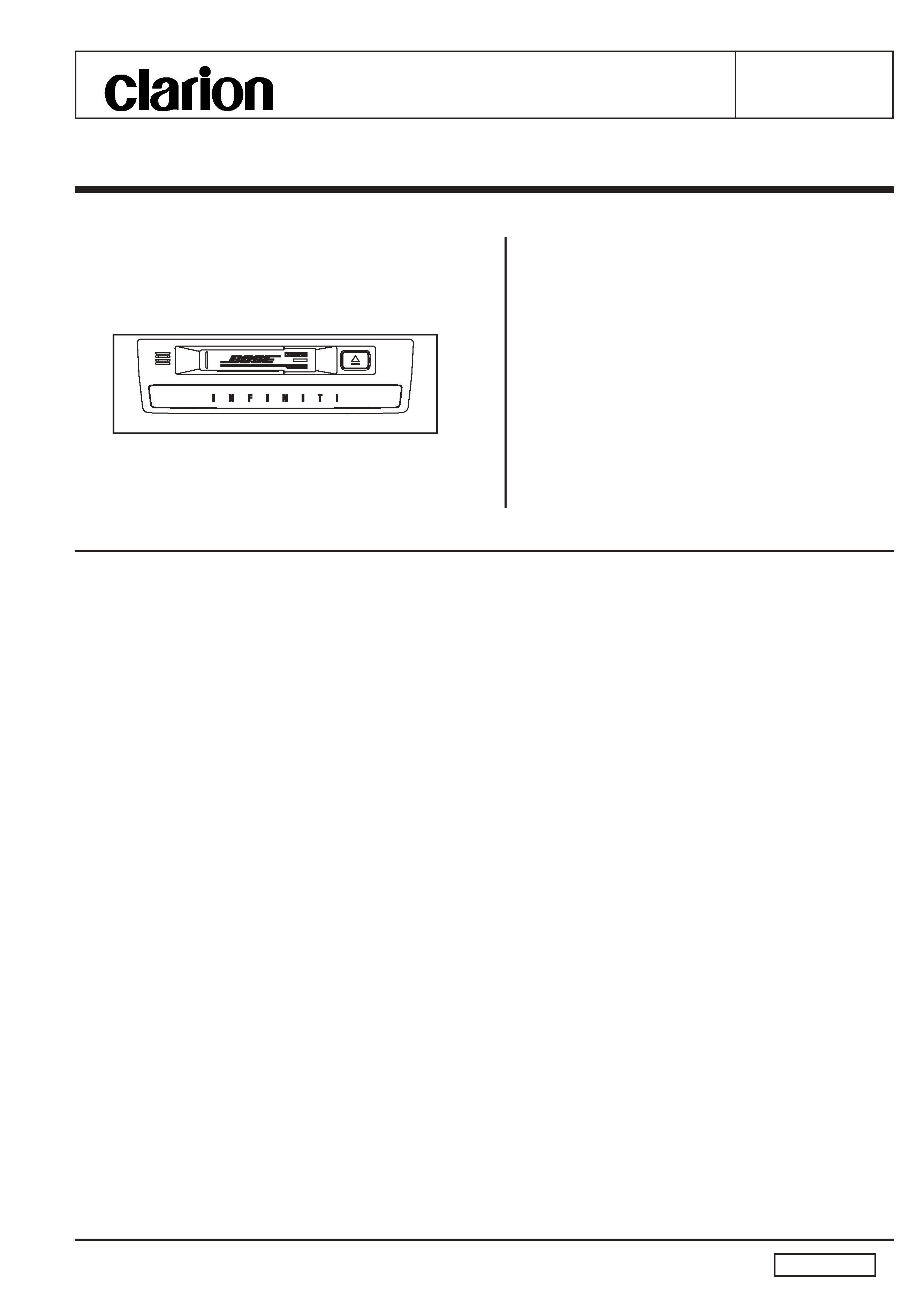
Service Manual
Model
NISSAN Automobile Genuine
AM/FM Radio Cassette Stereo
PN-1740B
(Genuine No.28115 CR900)
(ID No.CK080)
PN-1740K
(Genuine No.28115 AR260)
(ID No.CK100)
Model
SPECIFICATIONS
Radio section
Tuning system:
PLL Frequency synthesizer system
Receive range:
AM
530kHz to 1,710kHz
FM
87.9MHz to 107.9MHz
Intermediate frequency:
AM
450 +3/-3kHz
FM
10.7 +0.2/-0.2MHz
Quieting sensitivity:
AM
Less than 37dBu
(at 20dB S/N)
FM
Less than 15dBu
(at 30dB S/N)
Separation:
FM
More than 22 +5/-7dB(1kHz)
Auto tuning stop sensitivity:
AM
41 +6/-6dBu
(at 1000kHz,1400kHz)
FM
32 +6/-6dBu
Tape section
Reproducting system: 4 track 2 program
2 channel stereo system
Wow and flutter:
Less than 0.15%(W.R.M.S)
Separation:
More than 35dB
Cross talk:
More than 45dB
S/N ratio:
Normal tape(120us)
More than 47dB(DOLBY B NR off)
More than 55dB(DOLBY B NR on)
Metal tape(70us)
More than 49dB(DOLBY B NR off)
More than 57dB(DOLBY B NR on)
FF/REW time:
Less than 110sec.(C-60)
General
Load impedance:
4 ohm x4
Power output:
15W x4
Power supply voltage: DC13.2V(10.8V to 15.6V)
Negative ground
Consumptive current:
Less than 10A(MAX)
Dimensions(mm):
184(W) x56(H) x160(D)
Weight:
approx. 1.4kg
*
Dolby noise reduction manufactured under license from
Dolby Laboratories Licensing Corporation.
"DOLBY" and the double-D symbol are trademarks of
Dolby Laboratories Licensing Corporation.
*
Specifications and design are subject to change without
notice for further improvement.
COMPONENTS
PN-1740B-A/PN-1740K-A
Main unit
-----------
1
NOTE
*
We cannot supply PWB with component parts in prin-
ciple. When a circuit on PWB has failure,please repair it
by component parts base. Parts which are not mentioned
in service manual are not supplied.

- 2 -
PN-1740B,K
To engineers in charge of repair or
inspection of our products.
Before repair or inspection, make sure to follow
the instructions so that customers and Engineers
in charge of repair or inspection can avoid suf-
fering any risk or injury.
1. Use specified parts.
The system uses parts with special safety features against
fire and voltage. Use only parts with equivalent charac-
teristics when replacing them.
The use of unspecified parts shall be regarded as re-
modeling for which we shall not be liable. The onus of
product liability (PL) shall not be our responsibility in cases
where an accident or failure is as a result of unspecified
parts being used.
2. Place the parts and wiring back in their original positions
after replacement or re-wiring.
For proper circuit construction, use of insulation tubes,
bonding,gaps to PWB, etc, is involved. The wiring con-
nection and routing to the PWB are specially planned
using clamps to keep away from heated and high voltage
parts. Ensure that they are placed back in their original
positions after repair or inspection.
If extended damage is caused due to negligence during
repair, the legal responsibility shall be with the repairing
company.
3. Check for safety after repair.
Check that the screws, parts and wires are put back se-
curely in their original position after repair. Ensure for
safety reasons there is no possibility of secondary
ploblems around the repaired spots.
ADJUSTMENTS
This unit is not include control switching block so that used the special adjustment jig for measuring.
Switch of diversity
*
How to fix the MAIN channel.
While holding the buttons of M1 and M3, turn on the power switch of the jig.
*
How to fix the SUB channel.
While holding the buttons of M4 and M6, turn on the power switch.
*
To release the MAIN or SUB channel, turn off the power switch.
If extended damage is caused due to negligence of re-
pair, the legal responsibility shall be with the repairing
company.
4. Caution in removal and making wiring connection to the
parts for the automobile.
Disconnect the battery terminal after turning the ignition
key off. If wrong wiring connections are made with the
battery connected, a short circuit and/or fire may occur.
If extensive damage is caused due to negligence of re-
pair, the legal responsibility shall be with the repairing
company.
5. Cautions regarding chips.
Do not reuse removed chips even when no abnormality
is observed in their appearance. Always replace them
with new ones. (The chip parts include resistors, capaci-
tors, diodes, transistors, etc). The negative pole of tanta-
lum capacitors is highly susceptible to heat, so use spe-
cial care when replacing them and check the operation
afterwards.
6. Cautions in handling flexible PWB
Before working with a soldering iron, make sure that the
iron tip temperature is around 270 . Take care not to
apply the iron tip repeatedly(more than three times)to the
same patterns. Also take care not to apply the tip with
force.
7. Turn the unit OFF during disassembly and parts replace-
ment. Recheck all work before you apply power to the
unit.
Item
Procedure
Measuring
instrument
FM noise
convergence
MAIN channel
1. Connect to the jig and fix the MAIN channel to make the unit the test mode.
2. Radio is set to 98.1MHz in up down of the jig.
3. Set the output to 0dBm(0.775V) by main volume.
4. Input the 98.1MHz/55dBu(1kHz, 30% MOD, 22.5kHz Div.) SSG signal.
5. Adjust the outputs to -24dB by VR103 when the SG output is set to -20dBu.
SUB channel
1. Fix the SUB channel and follow the same adjustment steps as MAIN above.
2. Adjust the outputs to -19dB by VR101 when the SG output is set to -20dBu.
SSG
Milli-volt meter
FM SD
1. Input the 98.1MHz/32dBu(1kHz, 30% MOD, 22.5kHz Div.) signal.
2. Adjust the output of TP101 to become just high level with VR102.
SSG
Oscilloscope
Dolby level
1. Insert a Dolby level test tape(400Hz, 200nWb/m).
2. Adjust VR1(R)/VR2(L) so that an output of TP1(L)/TP2(R) is 300mV +1/-1dB.
Milli volt meter

- 3 -
PN-1740B,K
EXPLANATION OF IC
052-3160-21
MB90583CPFV-G-132
System Controller
1.Terminal Description
pin
1: INT 0
: IN : The initial setting input.
pin
2: NU
: - : Not in use.
pin
3: NU
: - : Not in use.
pin
4: NU
: - : Not in use.
pin
5: NU
: - : Not in use.
pin
6: TAPE RESET
: O : The reset signal output to the tape mech-
anism.
pin
7: J1850 ALE
: O : Address latch output to SAE-J1850 com-
munication protocol conformity transmis-
sion controller.
pin
8: J1850 RD
: IN : Read enable signal input from SAE-
J1850 communication protocol conformi-
ty transmission controller.
pin
9: GND
: - : Ground.
pin 10: J1850 WR
: IN : Write enable signal input from SAE-
J1850 communication protocol conformi-
ty transmission controller.
pin 11: DISC IND
: O : ON command output to the indicator for
"DISC".
pin 12: J1850 RESET
: O : Reset pulse output to SAE-J1850 com-
munication protocol conformity transmis-
sion controller.
pin 13: J1850 CS
: O : Chip select output to SAE-J1850 commu-
nication protocol conformity transmission
controller.
pin 14: NDS REQ 1
: IN : NDS request signal input.
pin 15: NDS REQ 2
: IN : NDS request signal input.
pin 16: NU
: - : Not in use.
pin 17: NU
: - : Not in use.
pin 18: NU
: - : Not in use.
pin 19: C-BUS SI
: IN : C-BUS serial data in.
pin 20: C-BUS SO
: O : C-BUS serial data out.
pin 21: VDD
: - : Positive supply voltage.
pin 22: C-BUS CLK
: O : C-BUS clock out.
pin 23: CD RESET
: O : The reset pulse output to the CD IC.
pin 24: C-BUS SRQ
: IN : C-BUS SRQ.
pin 25: CNNCT C
: - : Connect the capacitor.
pin 26: NDS SIG CHG : O : Analog signal changing command output
for NDS.
pin 27: NDS DAT CHG : O : Digital data changing command output for
NDS.
pin 28: VDD
: - : Positive supply voltage.
pin 29: GND
: - : Ground.
pin 30: NU
: - : Not in use.
pin 31: NU
: - : Not in use.
pin 32: VDD
: - : Positive supply voltage.
pin 33: VDD
: - : Positive supply voltage.
pin 34: GND
: - : Ground.
pin 35: GND
: - : Ground.
pin 36: NDS CHG SI
: IN : NDS serial data input.
pin 37: NDS CHG SO
: O : NDS serial data output.
pin 38: NU
: - : Not in use.
pin 39: NU
: - : Not in use.
pin 40: GND
: - : Ground.
pin 41: C-BUS RESET : O : C-BUS reset out.
pin 42: C-BUS SET
: O : C-BUS set out.
pin 43: NU
: - : Not in use.
pin 44: NU
: - : Not in use.
pin 45: TAPE EJECT
: IN : Tape eject signal input.
pin 46: RDS CLK
: IN : RDS clock pulse input.
pin 47: MC MODE 0
: IN : Micro computer mode select input.
pin 48: MC MODE 1
: IN : Micro computer mode select input.
pin 49: MC MODE 2
: IN : Micro computer mode select input.
pin 50: HSTXI
: - : HSTX input.
pin 51: J1850 INT
: IN : Interrupt command input from SAE-J1850
communication protocol conformity trans-
mission controller.
pin 52: ACC ON IN
: IN : ACC detection signal input.
pin 53: IVCS ON
: IN : IVCS ON.
pin 54: NU
: - : Not in use.
pin 55: NU
: - : Not in use.
pin 56: VDD DET
: IN : VDD detection signal input.
pin 57: DI
: IN : The serial data input.
pin 58: DO
: O : The serial data output.
pin 59: Clock Out
: O : Clock Out.
pin 60: CEO
: O : Chip enable output.
pin 61: RDS DATA
: IN : RDS serial data input.
pin 62: NU
: - : Not in use.
pin 63: NU
: - : Not in use.
pin 64: NU
: - : Not in use.
pin 65: NU
: - : Not in use.
pin 66: NU
: - : Not in use.
pin 67: NU
: - : Not in use.
pin 68: RESET
: O : Reset signal output.
pin 69: ANT ON
: O : Antenna ON command output.
pin 70: NU
: - : Not in use.
pin 71: NU
: - : Not in use.
pin 72: NU
: - : Not in use.
pin 73: AMP ON
: O : Audio power amplifier ON signal output.
pin 74: AF MUTE
: O : Audio frequency signal muting.
pin 75: RESET
: IN : Reset signal input.
pin 76: SYS ON
: O : System ON signal output.
pin 77: X1A
: - : The crystal connection.
pin 78: X0A
: - : The crystal connection.
pin 79: GND
: - : Ground.
pin 80: X0
: - : The crystal connection.
pin 81: X1
: - : The crystal connection.
pin 82: VDD
: - : Positive supply voltage.
pin 83: J1850 D 0
:I/O: Data input/output for SAE-J1850 commu-
nication protocol conformity transmission
controller.
pin 84: J1850 D 1
:I/O: Data input/output for SAE-J1850 commu-
nication protocol conformity transmission
controller.
pin 85: J1850 D 2
:I/O: Data input/output for SAE-J1850 commu-
nication protocol conformity transmission
controller.
pin 86: J1850 D 3
:I/O: Data input/output for SAE-J1850 commu-
nication protocol conformity transmission
controller.
pin 87: J1850 D 4
:I/O: Data input/output for SAE-J1850 commu-
nication protocol conformity transmission
controller.
pin 88: J1850 D 5
:I/O: Data input/output for SAE-J1850 commu-
nication protocol conformity transmission
controller.
pin 89: J1850 D 6
:I/O: Data input/output for SAE-J1850 commu-
nication protocol conformity transmission
controller.
pin 90: J1850 D 7
:I/O: Data input/output for SAE-J1850 commu-
nication protocol conformity transmission
controller.
pin 91: NU
: - : Not in use.
pin 92: NU
: - : Not in use.
pin 93: NU
: - : Not in use.
pin 94: NU
: - : Not in use.
pin 95: NU
: - : Not in use.
pin 96: NU
: - : Not in use.
pin 97: NU
: - : Not in use.
pin 98: NU
: - : Not in use.
pin 99: NU
: - : Not in use.
pin100: IF MUTE
: O : IF muting output.
- 4 -
PN-1740B,K
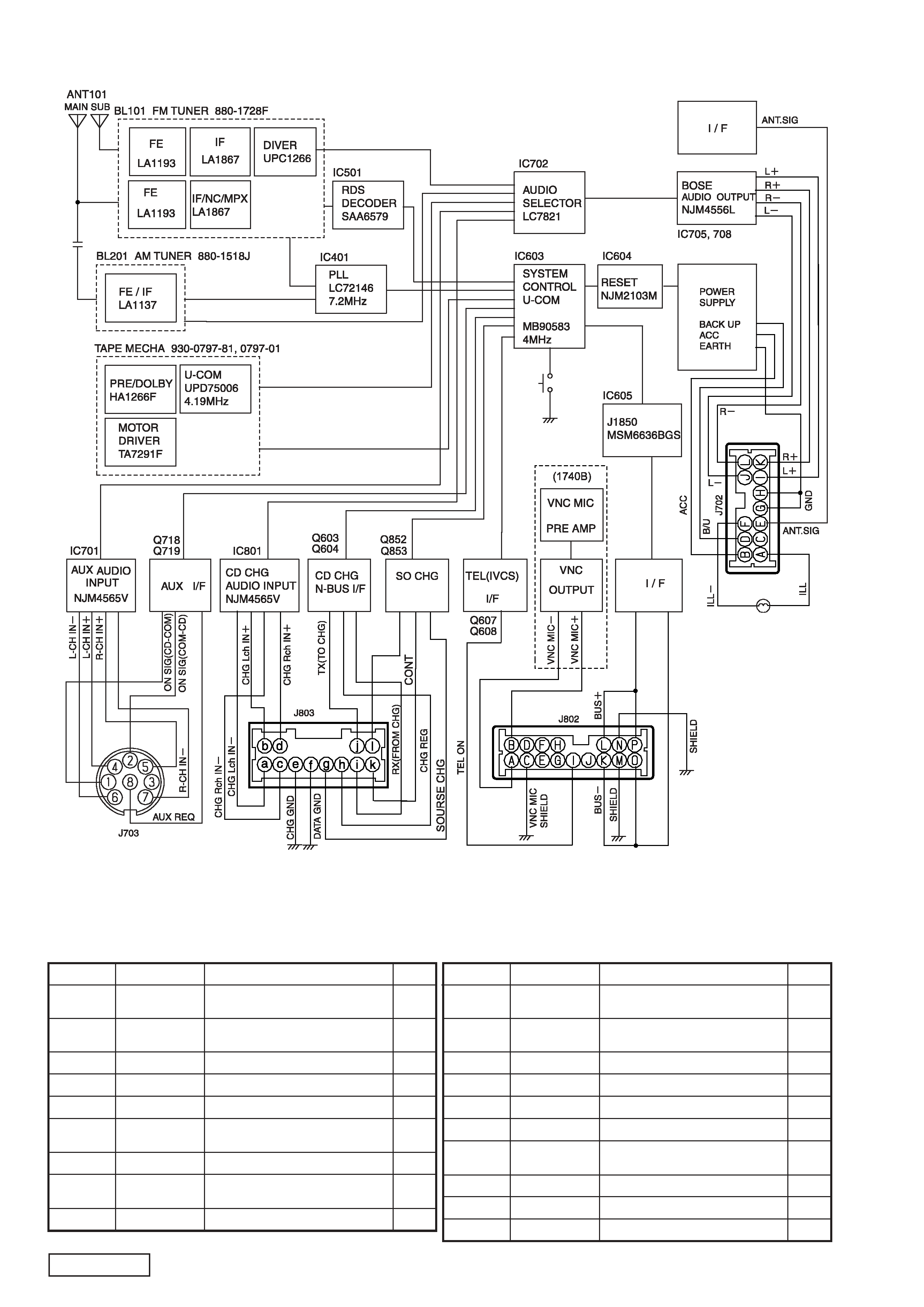
BLOCK DIAGRAM
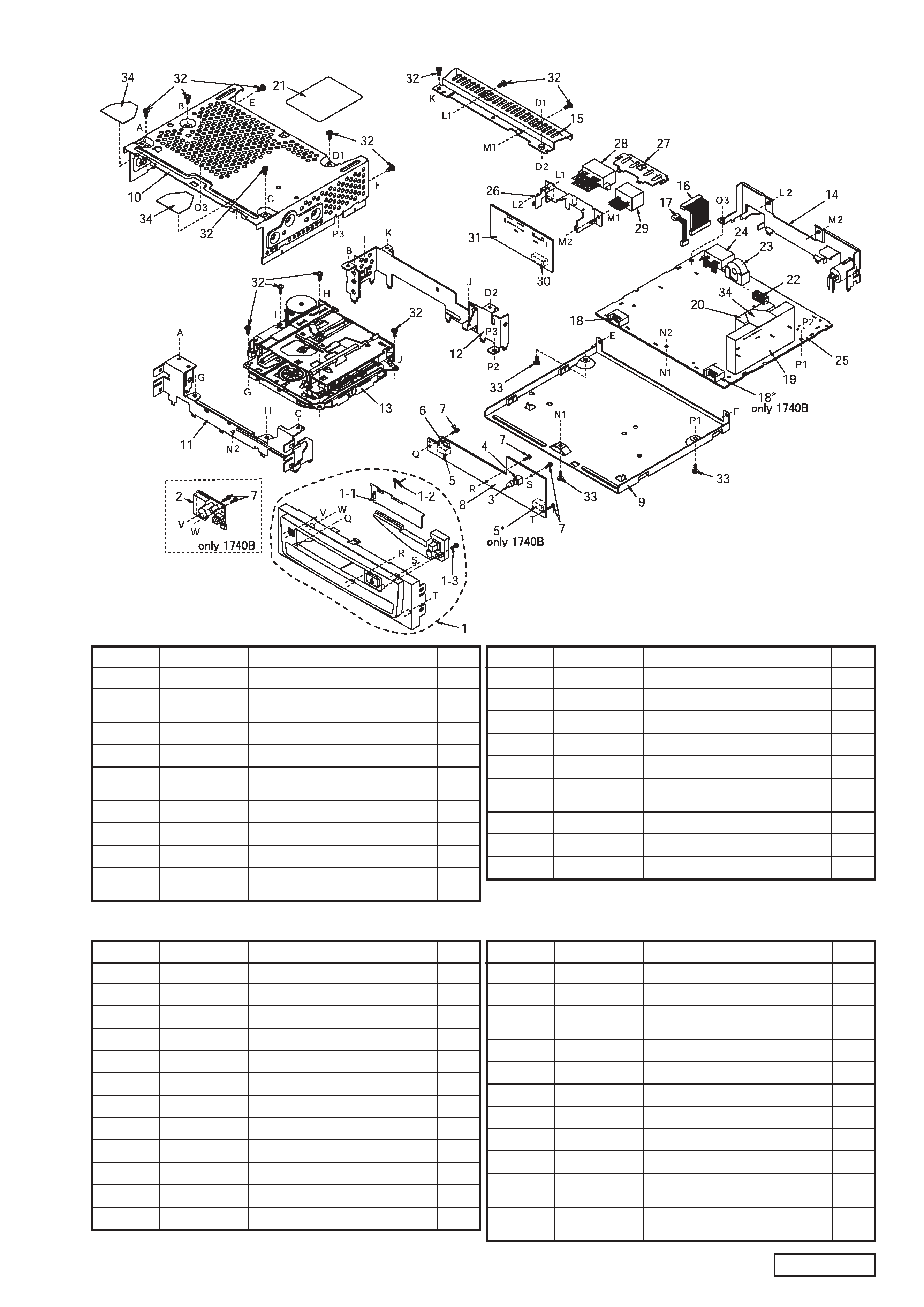
EXPLODED VIEW/PARTS LIST
Main section
Note)Several different parts of the same reference number are alternative parts.
One of those parts is used in the set.
Some parts depend on each model.The model name is specified in the description.
NO.
PART NO.
DESCRIPTION
Q'TY
NO.
PART NO.
DESCRIPTION
Q'TY
1
940-7944-42
ESCUTCHEON ASSY(1740B)
1
940-7944-52
ESCUTCHEON ASSY(1740K)
1-1
320-0457-48
DUSTPROOF COVER(1740B)
1
320-0457-49
DUSTPROOF COVER(1740K)
1-2
750-2626-00
SPRING
1
1-3
716-0778-00
WAVE SCREW(2 x6)
1
2
948-0602-00
MIC ASSY(1740B)
1
3
017-0420-33
14V40mA P.LAMP ORG.(1740B)
1
017-0420-26
14V40mA P.LAMP BLU.(1740K)
1
4
013-3934-02
SWITCH
1
5
074-1151-06
OUTLET SOCKET 6P(1740B)
2
074-1151-06
OUTLET SOCKET 6P(1740K)
1
6
076-0526-03
PLUG(3P)
1
7
716-0778-00
WAVE SCREW 2 x6(1740B)
6
716-0778-00
WAVE SCREW 2 x6(1740K)
4
8
039-1826-00
SWITCH PWB
1
(WITHOUT COMPONENT)
9
311-1758-02
LOWER CASE
1
10
310-1663-01
UPPER CASE
1
11
309-0732-01
FRONT PLATE
1
12
331-2471-20
MECHANISM BRACKET
1
13
930-0797-81
TAPE MECHANISM
1
930-0797-01
14
331-3040-10
REAR PLATE W/ANT PLUG
1
15
307-0672-00
REAR COVER
1
16
854-4457-01
EXTENSION LEAD(12P)
1
- 5 -
PN-1740B,K
NO.
PART NO.
DESCRIPTION
Q'TY
NO.
PART NO.
DESCRIPTION
Q'TY
17
854-4458-00
EXTENSION LEAD(3P)
1
18
076-0540-06
PLUG 6P(1740B)
2
076-0540-06
PLUG 6P(1740K)
1
19
880-1728F
TUNER PACK(FM)
1
20
880-1518J
TUNER PACK(AM)
1
21
286-9233-34
SETPLATE(1740B)
1
286-9233-35
SETPLATE(1740K)
22
076-0368-18
PLUG(18P)
1
23
010-8028-00
COIL
1
24
074-1284-00
OUTLET SOCKET
1
25
039-2221-00
MAIN PWB
1
(WITHOUT COMPONENT)
26
331-3041-00
OUTLET HOLDER A
1
27
331-3042-00
OUTLET HOLDER B
1
28
074-1268-10
OUTLET SOCKET
1
29
074-1013-30
OUTLET SOCKET
1
30
074-0898-18
OUTLET SOCKET(18P)
1
31
039-2222-00
SUB PWB
1
(WITHOUT COMPONENT)
32
714-2606-81
MACHINE SCREW(M2.6 x6)
13
33
716-1494-00
IT SCREW(M2.6 x6)
3
34
347-6521-00
SHIELD PART
3
Tape mechanism section
NO.
PART NO.
DESCRIPTION
Q'TY
NO.
PART NO.
DESCRIPTION
Q'TY
1
960-4294-22
DECK PLATE ASSY
1
2
960-4261-20
HEAD PLATE ASSY
1
3
960-4262-03
FF/REW-P-ASSY
1
4
960-4263-03
IDLER-P-ASSY F
1
5
960-4264-03
IDLER-P-ASSY R
1
6
960-4266-05
MODE PLATE ASSY
1
7
960-4269-05
ROLLER ASSY F
1
8
960-4270-05
ROLLER ASSY R
1
9
960-4348-03
REEL ASSY F
1
10
960-4349-03
REEL ASSY R
1
11
960-4389-03
EJECT SUB ASSY
1
11-1
750-3020-01
SWITCH PLATE SPRING
1
12
960-4338-09
BOTTOM SUB ASSY
1
12-1
960-4295-02
BOTTOM-P-ASSY
1
12-2
099-9926-01
FLEXIBLE PWB
1
(WITHOUT COMPONENT)
12-3
013-3951-32
SWITCH(MODE)
1
12-4
013-3953-01
SWITCH(METAL)
1
12-5
051-1776-00
IC
1
12-6
746-0767-00
WASHER
2
13
960-4282-06
DETECT SUB ASSY
1
14
960-4301-02
PLAY LINK ASSY
1
15
039-1365-00
SIDE PWB
1
(WITHOUT COMPONENT)
16
990-0698-00
REAR PWB ASSY
1
(WITH COMPONENT)