- 1 -
PN-2591M-G
Published by Service Dept.
Printed in Japan
Clarion Co., Ltd.
50 Kamitoda, Toda-shi, Saitama 335-8511 Japan
Service Dept.: 5-66 Azuma , Kitamoto-shi, Saitama 364-0007 Japan
Tel: +81-48-541-2335 / 2432 FAX: +81-48-541-2703
298-6177-00 Sep.2004
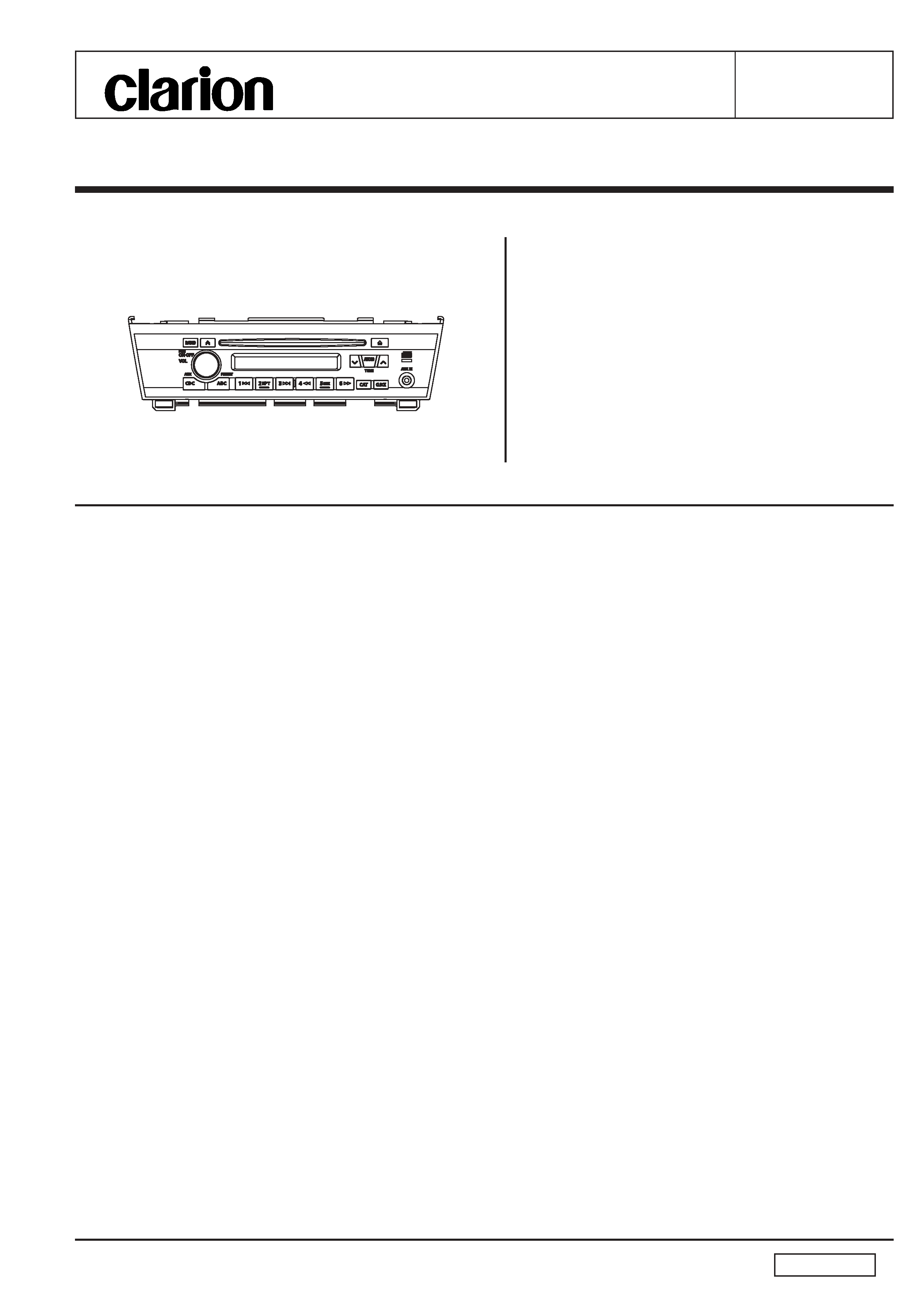
Service Manual
Model
NISSAN Automobile Genuine
FM/AM Radio CD Stereo
PN-2591M-G
(Genuine No.28185 6Z670)
(ID No.CY26A)
SPECIFICATIONS
Radio section
Tuning system:
PLL frequency synthesizer system
Receive range:
AM 530kHz to 1,710kHz
FM 87.75MHz,87.9 to 107.9MHz
Intermediate frequency:
AM 450+3/-3kHz
FM 10.7+0.3/-0.3MHz
Quieting sensitivity:
AM Less than 32dBu(at 20dB S/N)
FM Less than 10dBu(at 30dB S/N)
Separation:
FM More than 22+5/-7dB(1kHz)
S/N ratio:
AM More than 45dB
FM More than 50dB
Auto tuning stop sensitivity:
AM 32+6/-6dBu
(600/1000/1400kHz)
FM 25+6/-6dBu
(87.9/98.1/107.9MHz)
CD section
Disc:
12cm Disc
Separation:
More than 50dB(Filter:20kHz LPF)
S/N ratio:
More than 74dB
Distortion:
Less than 0.4%
(Filter:20kHz LPF)
General
Load impedance:
4 ohm/CH
Power output:
40W x 4
Power supply voltage: DC13.2V(10.8V to 16.0V)
Negative ground
Back-up consumption: Less than 3mA
Dimensions(mm):
180(W) x 52(H) x 159(D)
Weight:
1.35kg
NOTES
*
We cannot supply PWB with component parts in prin-
ciple. When a circuit on PWB has failure, please repair
it by component parts base. Parts which are not men-
tioned in service manual are not supplied.
*
Specifications and design are subject to change without
notice for further improvement.
COMPONENTS
PN-2591M-A,M-B,M-C
1.Main unit
-----------
1
To engineers in charge of repair or
inspection of our products.
Before repair or inspection, make sure to follow the
instructions so that customers and Engineers in
charge of repair or inspection can avoid suffering
any risk or injury.
1. Use specified parts.
The system uses parts with special safety features against
fire and voltage. Use only parts with equivalent character-
istics when replacing them.
The use of unspecified parts shall be regarded as remod-
eling for which we shall not be liable. The onus of product
liability (PL) shall not be our responsibility in cases where
an accident or failure is as a result of unspecified parts
being used.
2. Place the parts and wiring back in their original positions
after replacement or re-wiring.
- 2 -
PN-2591M-G
9. Cautions in handling the optical pickup
The laser diode of the optical pickup can be damaged by
electrostatic charge caused by your clothes and body. Make
sure to avoid electrostatic charges on your clothes or body,
or discharge static electricity before handling the optical
pickup.
9-1. Laser diode
The laser diode terminals are shorted for transporta-
tion in order to prevent electrostatic damage. After
replacement, open the shorted circuit. When remov-
ing the pickup from the mechanism, short the termi-
nals by soldering them to prevent this damage.
9-2. Actuator
The actuator has a powerful magnetic circuit. If a
magnetic material is put close to it. Its characteris-
tics will change. Ensure that no foreign substances
enter through the ventilation slots in the cover.
9-3. Cleaning the lens
Dust on the optical lens affects performance. To
clean the lens, apply a small amount of isopropyl
alcohol to lens paper and wipe the lens gently.
For proper circuit construction, use of insulation tubes,
bonding, gaps to PWB, etc, is involved. The wiring con-
nection and routing to the PWB are specially planned us-
ing clamps to keep away from heated and high voltage
parts. Ensure that they are placed back in their original
positions after repair or inspection.
If extended damage is caused due to negligence during
repair, the legal responsibility shall be with the repairing
company.
3. Check for safety after repair.
Check that the screws, parts and wires are put back se-
curely in their original position after repair. Ensure for safety
reasons there is no possibility of secondary ploblems
around the repaired spots.
If extended damage is caused due to negligence of repair,
the legal responsibility shall be with the repairing company.
4. Caution in removal and making wiring connection to the
parts for the automobile.
Disconnect the battery terminal after turning the ignition
key off. If wrong wiring connections are made with the bat-
tery connected, a short circuit and/or fire may occur. If ex-
tensive damage is caused due to negligence of repair, the
legal responsibility shall be with the repairing company.
5. Cautions regarding chips.
Do not reuse removed chips even when no abnormality is
observed in their appearance. Always replace them with
new ones. (The chip parts include resistors, capacitors,
diodes, transistors, etc). The negative pole of tantalum
capacitors is highly susceptible to heat, so use special care
when replacing them and check the operation afterwards.
6. Cautions in handling flexible PWB
Before working with a soldering iron, make sure that the
iron tip temperature is around 270 . Take care not to ap-
ply the iron tip repeatedly(more than three times)to the
same patterns. Also take care not to apply the tip with force.
7. Turn the unit OFF during disassembly and parts replace-
ment. Recheck all work before you apply power to the unit.
8. Cautions in checking that the optical pickup lights up.
The laser is focused on the disc reflection surface through
the lens of the optical pickup. When checking that the la-
ser optical diode lights up, keep your eyes more than 30cms
away from the lens. Prolonged viewing of the laser within
30cms may damage your eyesight.
ADJUSTMENT
FM noise
convergence
Item
Procedure
Measuring
instrument
1. Input the 98.1MHz/55dBu(1kHz 30% MOD) signal.
2. Adjust the outputs to -18+3/-3dB by VR102 when the SG output is set to -20dBu.
SSG
AC volt meter
Clock accuracy
1. Turn on the power switch, pressing the "M4" and "M2" button to make the unit the
test mode.
2. Set a universal timer to TP101(T-BASE), adjust TC101 so that a reading of the
meter is 0+0.2/-0 sec./day.
Universal timer

- 3 -
PN-2591M-G
EXPLANATION OF IC
052-3180-10
M30620MCA-8R3GP
System Controller
1.Terminal Description
pin
1: LCD CLK
: O : The clock pulse output to the LCD driver.
pin
2: LCD DO
: O : The srial data output to the LCD driver.
pin
3: LCD DI
: IN : The srial data input from the LCD driver.
pin
4: ILL PULSE
: IN : Illumination control signal input.
pin
5: TIME BASE
: IN : Time base pulse input.
pin
6: CNT GND
: - : Connect to the ground.
pin
7: CN VSS
: IN : Connect to VSS.
pin
8: TEST
: - : For the Test.
pin
9: ILL ON
: IN : Illumination ON signal input.
pin 10: RESET
: IN : Reset signal input.
pin 11: X OUT
: O : Crystal connection.
pin 12: GND
: - : Ground.
pin 13: X IN
: IN : Crystal connection.
pin 14: VDD
: - : Positive supply voltage.
pin 15: NU
: - : Not in use.
pin 16: BU DET
: IN : Backup detection signal input.
pin 17: ACC IN
: IN : ACC ON flag input.
pin 18: NU
: - : Not in use.
pin 19: SBSY
: IN : Sub code block synchronous signal input.
pin 20: AMP ON
: O : Audio power amplifier ON signal output.
pin 21: SYS ON
: O : System ON signal output.
pin 22: LCD ON
: O : LCD back light ON signal output.
pin 23: AF MUTE
: O : Audio frequency signal muting.
pin 24: BEEP
: O : Beep out.
pin 25: NU
: - : Not in use.
pin 26: NU
: - : Not in use.
pin 27: NU
: - : Not in use.
pin 28: CD ON
: O : CD ON signal output.
pin 29: NDS FLASH TX : O : NDS serial data output for external A/C.
pin 30: NDS FLASH RX : IN : NDS serial data input for external A/C.
pin 31: FLASH CLK
: O : The clock pulse output for the flash mem-
ory.
pin 32: NU
: - : Not in use.
pin 33: NU
: - : Not in use.
pin 34: NU
: - : Not in use.
pin 35: NDS CNT
: O : Low = A/C 1, High = A/C 2.
pin 36: NDS REQ 2
: IN : NDS request signal input.
pin 37: NDS REQ 1
: IN : NDS request signal input.
pin 38: SOURCE CHG : O : The signal source change signal output.
pin 39: FLASH EPM
: O : FLASH EPM.
pin 40: VOL DO
: O : Serial data output to the volume IC.
pin 41: VOL CLK
: O : The clock pulse output to the volume IC.
pin 42: VOL CE
: O : The chip enable signal output to the vol-
ume IC.
pin 43: NU
: - : Not in use.
pin 44: FLASH CE
: O : The chip enable signal output to the flash
memory.
pin 45: NU
: - : Not in use.
pin 46: JACK ON
: IN : AUX detection signal input.
pin 47: NU
: - : Not in use.
pin 48: CD CONNECT
: IN : CD connection check signal input.
pin 49: BUC 0
:I/O: CD IC Data input / output.
pin 50: BUC 1
:I/O: CD IC Data input / output.
pin 51: BUC 2
:I/O: CD IC Data input / output.
pin 52: BUC 3
:I/O: CD IC Data input / output.
pin 53: BUC CLOCK
: O : CD IC clock pulse output.
pin 54: CCE
: O : The chip enable signal output.
pin 55: CD RESET
: O : The reset pulse output to the CD IC.
pin 56: S STOP
: IN : Inside limit signal input from the CD mech-
anism.
pin 57: CHU SW
: IN : CD disc chucking signal input.
pin 58: TR A
: IN : Photo sensor signal input from the CD
mechanism.
pin 59: TR B
: IN : Photo sensor signal input from the CD
mechanism.
pin 60: VDD
: - : Positive supply voltage.
pin 61: LD CONT
:I/O: Loading motor control signal input/output.
pin 62: GND
: - : Ground.
pin 63: PLL CE
: O : The chip enable signal output to the PLL
IC.
pin 64: PLL CLK
: O : The clock pulse output to the PLL IC.
pin 65: PLL DO
: O : Serial data output to the PLL IC.
pin 66: PLL DI
: IN : Serial data input from the PLL IC.
pin 67: ST/TWEET
:I/O: Outputs "L" at AM 900kHz receiving. Inputs
"L" at FM stereo receiving.
pin 68: LD MUTE
: O : Muting signal output to the CD mechanism.
pin 69: RADIO ON
: O : Radio ON flag output.
pin 70: NU
: - : Not in use.
pin 71: NU
: - : Not in use.
pin 72: NU
: - : Not in use.
pin 73: NU
: - : Not in use.
pin 74: NU
: - : Not in use.
pin 75: NU
: - : Not in use.
pin 76: NU
: - : Not in use.
pin 77: NU
: - : Not in use.
pin 78: NU
: - : Not in use.
pin 79: NU
: - : Not in use.
pin 80: NU
: - : Not in use.
pin 81: NU
: - : Not in use.
pin 82: NU
: - : Not in use.
pin 83: NU
: - : Not in use.
pin 84: NU
: - : Not in use.
pin 85: VOL 1
: IN : Volume control pulse input from the rotary
encoder.
pin 86: VOL 2
: IN : Volume control pulse input from the rotary
encoder.
pin 87: NU
: - : Not in use.
pin 88: NU
: - : Not in use.
pin 89: CD EJECT
: IN : CD eject switch signal input.
pin 90: NU
: - : Not in use.
pin 91: ILL DET
: IN : Illumination ON signal input.
pin 92: NU
: - : Not in use.
pin 93: NU
: - : Not in use.
pin 94: A VSS
: - : Analog ground.
pin 95: NU
: - : Not in use.
pin 96: Vref
: - : Reference voltage.
pin 97: A VCC
: - : Positive supply voltage for the internal an-
alog section.
pin 98: POWER SW
: IN : Power switch ON signal input.
pin 99: LCD RESET
: O : Reset pulse output to LCD.
pin100: LCD CE
: O : The chip enable signal output to the LCD
driver.
- 4 -
PN-2591M-G
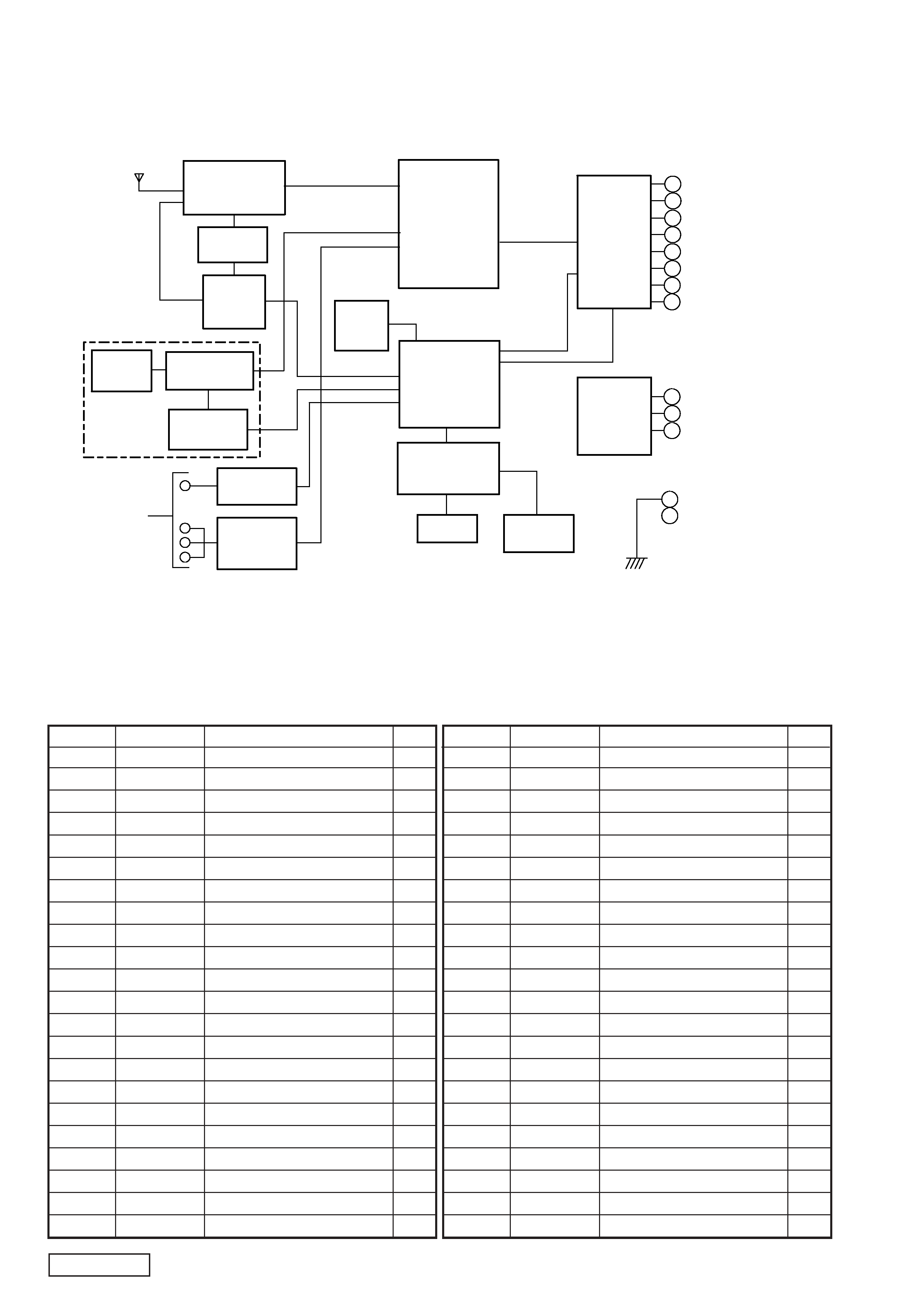
BLOCK DIAGRAM
Main section
BL101
AM / FM TUNER
880-1921R
IC302
ELECTRICAL
VOLUME
BASS / TREBLE
BAL / FAD
LC75412
IC506
POWER IC
40W x 4CH
TA8275H
CD MECHANISM
RF-AMP
TA2157F
DSP/SSP/DAC
TC94A14FA
IC202
RESET
S80933
IC201
M30620MCA
IC1101
LCD DRIVER
LC75883
LCD
K
G
L
H
D
E
F
B
O
I
J
P
ANT101
CONTROLLER
DRIVER
BA5983FP
POWER
SUPPLY
KEY
MATRIX
GND
GND
C
Q202, 203
L.P.F
IC102
PLL-IC
LC72191
MINI-JACK
DETECT SW
IC901
AUX-AMP
NJM4565V
J1102
AUX INPUT
MINI JACK
FRONT SP L-CH(-)
FRONT SP L-CH(+)
FRONT SP R-CH(-)
FRONT SP R-CH(+)
REAR SP L-CH(-)
REAR SP L-CH(+)
REAR SP R-CH(-)
REAR SP R-CH(+)
ILLUMI(-)
ILLUMI(+)
ACC
J701
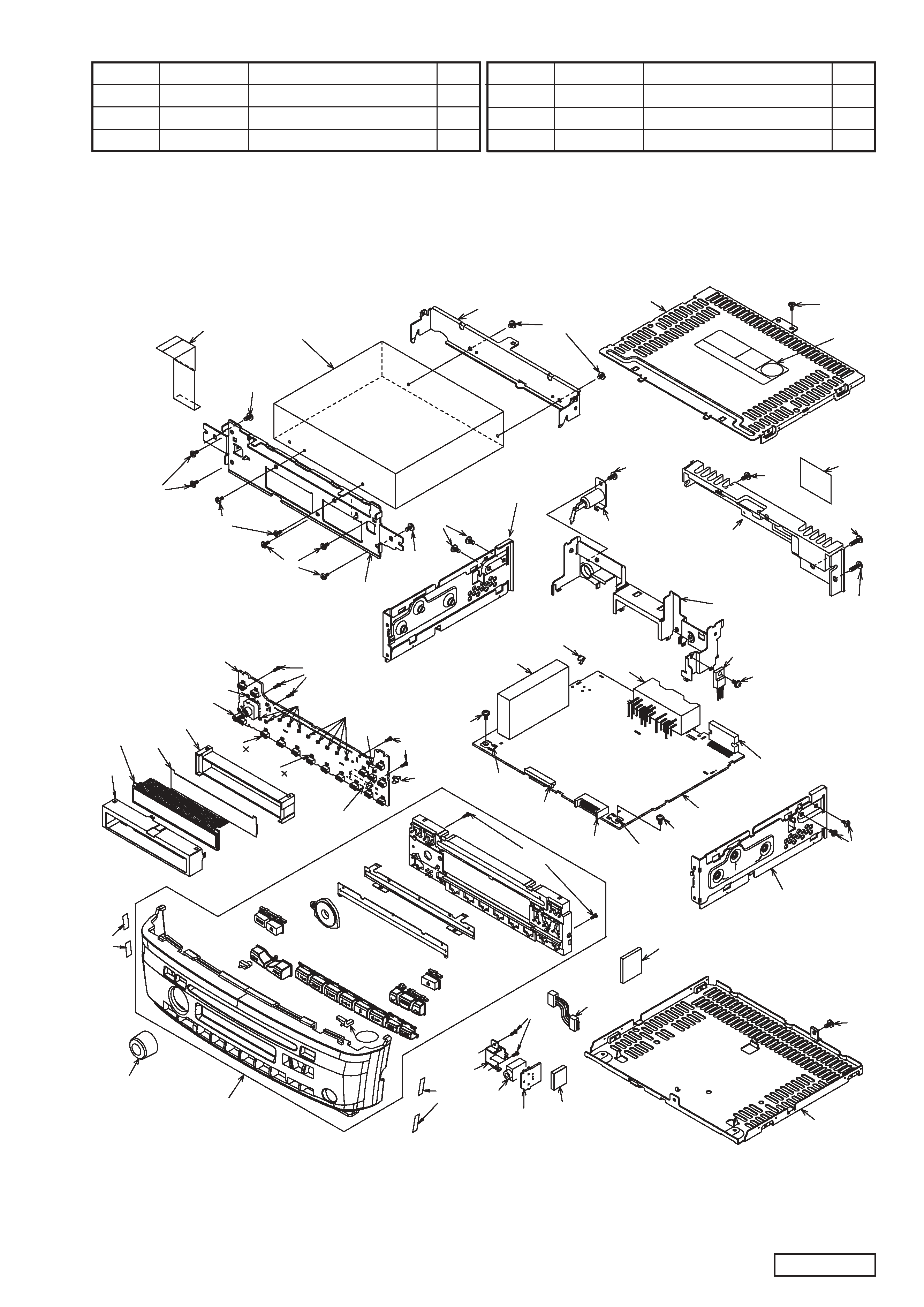
EXPLODED VIEW/PARTS LIST
Main section
22
714-2603-81
MACHINE SCREW(M2.6 x 3)
2
23
702-3008-81
TAP SCREW
2
24
347-5206-00
SHIELD SHEET
1
25
345-5325-00
CUSHION RUBBER
1
26
-----------
MAIN PWB
1
27
076-0648-20
PLUG(20P)
1
28
074-1191-26
OUTLET SOCKET(26P)
1
29
103-2012-00
TRANSISTOR
1
30
051-2042-00
IC(TA8275H)
1
31
074-1068-11
OUTLET SOCKET
1
32
880-1921R
AM/FM TUNER
1
33
073-0762-90
TERMINAL
2
34
307-0683-05
REAR PLATE
1
35
313-1931-10
HEAT SINK
1
36
092-0702-00
ANT RECEPT
1
37
716-0878-00
IT SCREW(M2.6 x 5)
3
38
714-2606-81
MACHINE SCREW(M2.6 x 6)
15
39
714-2612-81
MACHINE SCREW(M2.6 x 12)
2
40
073-0774-00
TERMINAL
1
41
305-0316-00
SIDE PLATE(L)
1
42
305-0317-00
SIDE PLATE(R)
1
43
331-3624-00
ES-PLATE
1
1
940-8019-75
ESCUTCHEON ASSY
1
1-1
716-0872-00
PAD SCREW
2
2
331-3621-00
LCD COVER
1
3
379-1268-30
LCD INDICATOR
1
4
335-6968-00
COLOR FILTER
1
5
335-6967-80
LCD HOLDER
1
6
-----------
SWITCH PWB
1
7
016-0010-09
VR-W/SHAFT
1
8
001-7063-91
LED(YEL)
18
9
001-7048-96
LED(YEL)
11
10
013-6302-50
SWITCH
16
11
074-1279-70
OUTLET SOCKET(20P)
1
12
073-0774-00
TERMINAL
1
13
075-0306-00
JACK
1
14
331-3623-00
JACK HOLDER
1
15
854-4562-00
EXTENSION LEAD
1
16
076-0478-55
PLUG
1
17
380-5562-80
KNOB
1
18
716-0872-00
PAD SCREW(M1.7 x 5)
5
19
347-2510-00
CUSHION TAPE
4
20
345-5324-00
CUSHION RUBBER
1
21
716-0778-00
WAVE SCREW
2
NO.
PART NO.
DESCRIPTION
Q'TY
NO.
PART NO.
DESCRIPTION
Q'TY
- 5 -
PN-2591M-G
NO.
PART NO.
DESCRIPTION
Q'TY
NO.
PART NO.
DESCRIPTION
Q'TY
44
929-0220-86
CD MECHANISM
1
45
331-3254-20
MECH-BRACKET
1
46
816-2549-00
FLAT WIRE
1
47
311-1833-20
LOWER CASE
1
48
310-1739-20
UPPER CASE
1
49
286-9269-35
SETPLATE
1
1-1
46
44
23
38
38
38
43
23
38
41
45
22
48
38
49
24
38
35
39
39
38
36
34
29
37
30
31
40
32
37
33
28
27
33
37
26
38
42
38
47
25
15
20
21
14
13
6
19
1
17
19
2
3
4
5
7
6
18
10 16
18
12
8 18
9
9
9
16
11