- 1 -
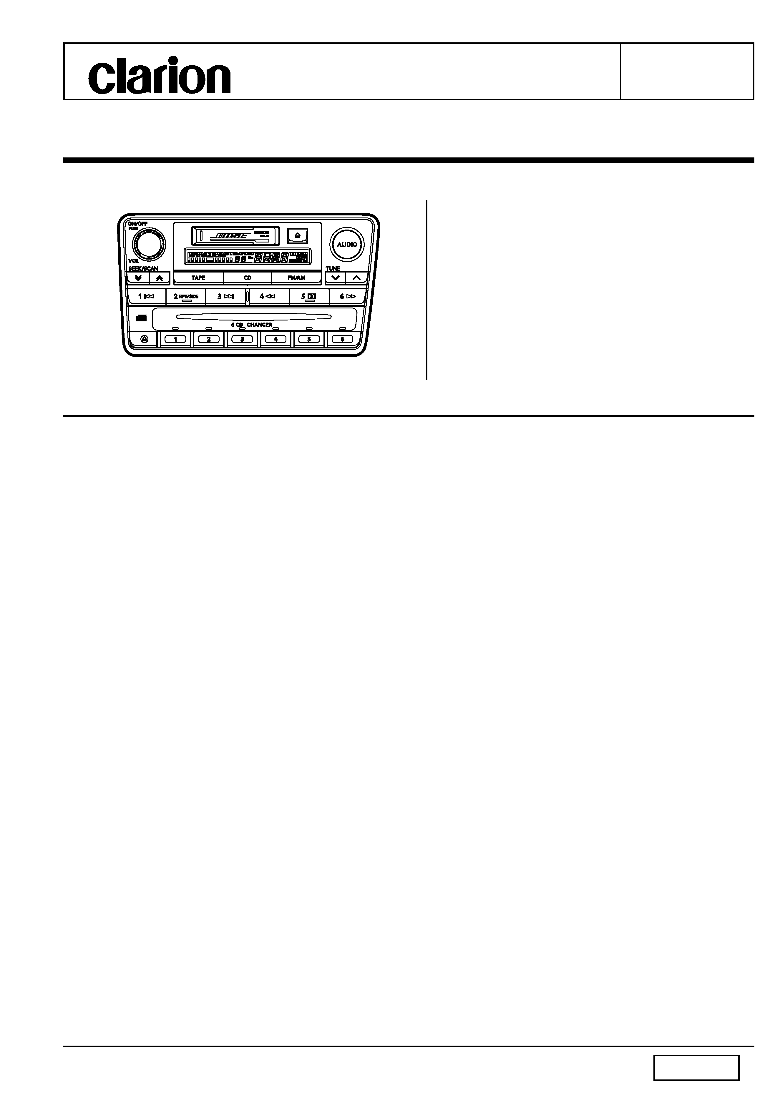
PN-2411N /
PN-2430N
NISSAN Automobile Genuine
AM/FM Radio 6-Disc CD Changer/
Cassette deck
PN-2411N
Published by Service Dept.
Printed in Japan
Clarion Co., Ltd.
22-3, Shibuya 2-chome, Shibuyaku, Tokyo, 150-8335 Japan
Service Dept.- 50 kamitoda,Toda-shi,Saitama,335-8511 Japan Tel: 048-443-1111
FAX:048-433-6996
298-5895-00 Jan.2001 B
Service Manual
Model
PN-2430N
SPECIFICATIONS
Radio section
Tuning system:
PLL Frequency synthesizer system
Receive range:
AM 530kHz to 1,710kHz(2411N)
FM 87.9MHz to 107.9MHz(2411N)
AM 531kHz to 1,602kHz(2430N)
FM 87.5MHz to 107.9MHz(2430N)
Intermediate frequency:
AM
450
3kHz
FM
10.7
0.2MHz
Quieting sensitivity:
AM
Less than 32dB
(at 20dB S/N)
FM
Less than 10dB
(at 30dB S/N)
Separation:
FM
More than 20dB(at 1kHz)
Auto tuning stop sensitivity:
AM
32
6dB
FM
25
6dB
CD section
Disc:
Compact disc(12cm)
Separation:
More than 52dB
(at 1kHz,0dB Disc,20kHz LPF)
S/N ratio:
More than 80dB
Distortion:
Less than 0.2%
(at 1kHz,0dB Disc,20kHz LPF)
Tape section
Reproducting system: 4 track 2 program
2 channel stereo system
Wow and flutter:
Less than 0.15
(W.R.M.S)
Separation:
More than 35dB
Crosstalk:
More than 45dB
S/N ratio:
Normal tape(120
s)
More than 55dB
(DOLBY B NR OFF)
More than 63dB
(DOLBY B NR ON)
Metal tape(70
s)
More than 57dB
(DOLBY B NR OFF)
More than 65dB
(DOLBY B NR ON)
FF/REW time:
Less than 110sec.(C-60)
General
Load impedance:
300
/CH
Output level(BOSE 6V output specification):
6V+0.5V/-2.0V(1kHz CD 0dB)
Power supply voltage: DC14.4V(10.8V to 15.6V)
Negative ground
Consumptive current:
2.7mA(Back up)
Dimensions(mm):
220.4(W)
118.8(H)
185(D)
Weight:
3.5kg
Dolby noise reduction manufactured under license from
Dolby Laboratories Licensing Corporation.
"DOLBY" and the double-D symbol are trademarks of
Dolby Laboratories Licensing Corporation.
Specifications and design are subject to change without
notice for further improvement.
NOTE
We can not supply PWB with component parts in prin-
ciple. When a circuit on PWB has failure, please repair
it by component parts base. Parts which are not men-
tioned in service manual are not supplied.
COMPONENT
PN-2411N-A/PN-2430N-A
Main unit
1
(Genuine No.28188 3W705/ID No.CNB78)
Model
(Genuine No.28188 5W310/ID No.CNJ78)

- 2 -
PN-2411N /
PN-2430N
To engineers in charge of repair or
inspection of our products.
Before repair or inspection, make sure to follow
the instructions so that customers and Engineers
in charge of repair or inspection can avoid suf-
fering any risk or injury.
1. Use specified parts.
The system uses parts with special safety features against
fire and voltage. Use only parts with equivalent charac-
teristics when replacing them.
The use of unspecified parts shall be regarded as re-
modeling for which we shall not be liable. The onus of
product liability (PL) shall not be our responsibility in cases
where an accident or failure is as a result of unspecified
parts being used.
2. Place the parts and wiring back in their original positions
after replacement or re-wiring.
For proper circuit construction, use of insulation tubes,
bonding, gaps to PWB, etc, is involved. The wiring con-
nection and routing to the PWB are specially planned
using clamps to keep away from heated and high voltage
parts. Ensure that they are placed back in their original
positions after repair or inspection.
If extended damage is caused due to negligence during
repair, the legal responsibility shall be with the repairing
company.
3. Check for safety after repair.
Check that the screws, parts and wires are put back se-
curely in their original position after repair. Ensure for
safety reasons there is no possibility of secondary
ploblems around the repaired spots.
If extended damage is caused due to negligence of re-
pair, the legal responsibility shall be with the repairing
company.
4. Caution in removal and making wiring connection to the
parts for the automobile.
Disconnect the battery terminal after turning the ignition
key off. If wrong wiring connections are made with the
battery connected, a short circuit and/or fire may occur.
If extensive damage is caused due to negligence of re-
pair, the legal responsibility shall be with the repairing
company.
5. Cautions regarding chips.
Do not reuse removed chips even when no abnormality
is observed in their appearance. Always replace them
with new ones. (The chip parts include resistors, capaci-
tors, diodes, transistors, etc). The negative pole of tanta-
lum capacitors is highly susceptible to heat, so use spe-
cial care when replacing them and check the operation
afterwards.
6. Cautions in handling flexible PWB
Before working with a soldering iron, make sure that the
iron tip temperature is around 270
. Take care not to
apply the iron tip repeatedly(more than three times)to the
same patterns. Also take care not to apply the tip with
force.
7. Turn the unit OFF during disassembly and parts replace-
ment. Recheck all work before you apply power to the
unit.
8. Cautions in checking that the optical pickup lights up.
The laser is focused on the disc reflection surface through
the lens of the optical pickup. When checking that the
laser optical diode lights up, keep your eyes more than
30cms away from the lens. Prolonged viewing of the la-
ser within 30cms may damage your eyesight.
9. Cautions in handling the optical pickup
The laser diode of the optical pickup can be damaged by
electrostatic charge caused by your clothes and body.
Make sure to avoid electrostatic charges on your clothes
or body, or discharge static electricity before handling the
optical pickup.
9-1. Laser diode
The laser diode terminals are shorted for transpor-
tation in order to prevent electrostatic damage.
After replacement, open the shorted circuit. When
removing the pickup from the mechanism, short
the terminals by soldering them to prevent this
damage.
9-2. Actuator
The actuator has a powerful magnetic circuit. If a
magnetic material is put close to it. its characteris-
tics will change. Ensure that no foreign substances
enter through the ventilation slots in the cover.
9-3. Cleaning the lens
Dust on the optical lens affects performance. To
clean the lens, apply a small amount of isopropylalcohol
to lens paper and wipe the lens gently.
ADJUSTMENTS
Switch of diversity
How to fix the MAIN channel.
While holding the buttons of CH1 and CH3, turn on the power switch.
How to fix the SUB channel.
While holding the buttons of CH4 and CH6, turn on the power switch.
To release the MAIN or SUB channel, turn off the power switch.
Item
Procedure
Measuring
instrument
FM noise
convergence
MAIN channel
1. Fix to MAIN channel and set the main volume to 0dB(245mV).
2. Input the 98.1MHz/55dB
(1kHz, 30% MOD.) SSG signal.
3. Adjust the outputs to
14
1dB by VR102 when the SG output is set
20dB
.
SUB channel
1. Follow the same adjustment steps as MAIN above. (with VR101)
SSG
Milli-volt meter
FM SD
1. Input a 98.1MHz/25dB
(1kHz, 30% MOD.) signal.
2. Adjust VR103 to obtain the output level of TP101(SD) become just high.
SSG
Oscilloscope
Dolby level
1. Insert a Dolby level test tape(400Hz, 200nWb/m).
2. Adjust VR1(L)/VR2(R) so that an output of TP202(L)/TP201(R) is 300mV
1dB.
Milli volt meter
- 3 -
PN-2411N /
PN-2430N
EXPLANATION OF IC
052-1164-30
PD17718GC-542-3B9
NDS Tuner/Tape/CD Auto Changer Controller
1.Terminal Description
pin
1 : ACC IN_
: IN : Acc-ON-signal input. Negative logic.
pin
2 : TAPE IN
: IN : Tape loading start signal input.
pin
3 : TAPE EJ_
: IN : Tape-eject-signal input. Negative logic.
pin
4 : VOL 1
: IN : Main volume control signal input.
pin
5 : VOL 2
: IN : Main volume control signal input.
pin
6 : LCD INH_
: O : Inhibit signal output to LCD driver.
Negative logic.
pin
7 : LCD CE
: O : Chip-enable signal output to LCD driv-
er.
pin
8 : LCD CLK
: O : Serial data clock output to LCD driver.
pin
9 : LCD DO
: O : Serial data output to LCD driver.
pin 10 : KO 0
: O : Key scan signal output.
pin 11 : KO 1
: O : Key scan signal output.
pin 12 : KO 2
: O : Key scan signal output.
pin 13 : KO 3
: O : Key scan signal output.
pin 14 : KO 4
: O : Key scan signal output.
pin 15 : POWER SW_
: IN : Power Key input(alternative).
Negative logic.
pin 16 : ANT ON
: O : Antenna ON signal output.
pin 17 : LCD ON_
: O : LCD back light ON signal output.
Negative logic.
pin 18 : SYS ON
: O : System-ON signal output. (Hi-Z)
pin 19 : FM ON
: O : FM-ON signal output. (Hi-Z)
pin 20 : AM ON
: O : AM-ON signal output. (Hi-Z)
pin 21 : GND
: - : Ground.
pin 22 : KI 3
: IN : Key scan signal input.
pin 23 : KI 2
: IN : Key scan signal input.
pin 24 : KI 1
: IN : Key scan signal input.
pin 25 : KI 0
: IN : Key scan signal input.
pin 26 : ST ON_
: IN : Stereo ON signal input. Negative logic.
pin 27 : REEL PULS
: IN : Reel pulse input.
pin 28 : AM IF
: IN : AM-IF counter input.
pin 29 : FM IF
: IN : FM-IF counter input.
pin 30 : VDD
: - : Positive supply voltage.
pin 31 : FM OSC
: IN : FM VCO ( Local Oscillation ) input.
pin 32 : AM OSC
: IN : AM VCO ( Local Oscillation ) input.
pin 33 : GND
: - : Ground.
pin 34 : NU
: O : Not in use.
pin 35 : EO
: O : Error out terminal.
pin 36 : GND
: - : Ground.
pin 37 : RF MUTE
: O : IF-output control. Output "H" in SEEK.
pin 38 : SUB
: O : "H" = FM Sub fixed.
pin 39 : TWEET
: O : In AM mode, Output "L" in receiving
900kHz.
In FM mode, Output "H" in Main-fixed
mode.
pin 40 : BEEP
: O : Beep out.
pin 41 : NU
: IN : Not in use.
pin 42 : TEL ON_
: IN : TEL-on signal input. Negative logic.
pin 43 : DOLBY
: O : "H" = DOLBY on.
pin 44 : T/R
: O : "H" = Mechanism mute on.
pin 45 : F/R
: O : "H" = forward ( Tape ).
"L" = reverse ( Tape ).
pin 46 : MS
: IN : Music sensing signal input.
"H" = non-recorded part.
pin 47 : S SEEK Down : IN : "Seek / APS up" signal input from the
remote controller.
pin 48 : BIT 3
: IN : Mechanism mode switch signal input.
Ref. Table 1.
pin 49 : BIT 2
: IN : Mechanism mode switch signal input.
Ref. Table 1.
pin 50 : BIT 1
: IN : Mechanism mode switch signal input.
Ref. Table 1.
pin 51 : MSGV
: O : Music sensing amplifier sensitivity con-
trol signal output.
"H" = play, "L" = FF/Rew.
pin 52 : M-MOTOR
: O : "H" = Main motor on.
pin 53 : P 2
: O : Power motor control.
Ref. Table 2.
pin 54 : P 1
: O : Power motor control.
Ref. Table 2.
pin 55 : VOL STB 2
: O : STB2 output for electric volume IC
TC9412F.
pin 56 : VOL STB 1
: O : STB1 output for electric volume IC
LC75386.
pin 57 : VOL CLK
: O : Serial data clock output for electric vol-
ume IC.
pin 58 : VOL DATA
: O : Serial data output for electric volume
IC.
pin 59 : R MUTE
: IN : Rear channel mute signal output.
pin 60 : AMP ON
: O : "H" = Power amplifier on.
pin 61 : R VOL UP
: IN : Remote control volume input.
pin 62 : R VOL DW
: IN : Remote control volume input.
pin 63 : AM NC
: O : "High Z"= AM noise canceler ON.
pin 64 : AUX REQ
: O : AUX request signal output. (high Z)
pin 65 : R MODE
: IN : Mode change signal input from the re-
mote controller.
pin 66 : R SEEK UP
: IN : Seek or APS up signal input from the
remote controller.
pin 67 : F MUTE
: IN : Front channel mute signal output.
pin 68 : NDS REQ
: IN : Request input from NDS-A/C.
pin 69 : NDS TXD
: O : TX output to NDS-A/C.
pin 70 : NDS RXD
: IN : RX input from NDS-A/C.
pin 71 : AUX ON_
: IN : AUX ON signal input. Negative logic.
pin 72 : COMBI ON
: O : Combi ON flag output. Negative logic.
pin 73 : NAVI ON_
: IN : Navigation ON signal input.
pin 74 : REG
: - : Connects a capacitor to reduce voltage
regulator ripple.
pin 75 : GND
: - : Ground.
pin 76 : XOUT
: O : Connects a crystal.
pin 77 : XIN
: IN : Connects a crystal.
pin 78 : CE
: IN : Chip enable signal input.
pin 79 : VDD
: - : Positive supply voltage.
pin 80 : RESET_
: IN : Reset signal input. Negative logic.
Table 1.Mechanism mode switch
Mechanism mode
Bit1(pin50)
Bit2(pin49)
Bit3(pin48)
Eject
H
H
H
Loading
H
H
L
Stop
L
H
L
Fwd-FF ( Rev-Rew )
L
L
H
Fwd-Rew ( Rev-FF )
H
L
L
Fwd-Play
H
L
H
Rev-Play
L
H
H
Table 2.Power motor control
Mechanism mode
P1(pin54)
P2(pin53)
Loading, Head advance
H
L
Eject, Head retreat
L
H
Keeping a state
H
H
Stop
L
L
2. Key matrix
Table
3. Key matrix table
KI 0
KI 1
KI 2
KI 3
(pin 25)
(pin 24)
(pin 23)
(pin 22)
KO 0
FM/AM
Tape/CD
Seek/Scan up
Seek/Scan down
(pin10)
Tape(2DIN)
Clock
KO 1
M 1
M 2
M 3
CD(2DIN)
(pin11)
APS Rew
Prog
APS FF
KO 2
M 4M 5M 6
(pin12)
Rew
DOLBY
FF
KO 3
Sound
Tune/Disk up
Tune/Disk down
(pin13)
M
H
Sound up
Sound down
KO 4
Clock
1DIN/2DIN
Tel Vol
(pin14)
(Diode sw)
(Diode sw)
(Diode sw)
3. Diode switches
A. Clock
OFF
: Without Clock.
ON
: With Clock.
B. 1DIN/2DIN
OFF
: 1-DIN
ON
: 2-DIN

- 4 -
PN-2411N /
PN-2430N
C. Tel Vol
OFF
: Tel Vol
ON
: Non Tel Vol
4. Treasured Key method
A. Display the version of the Micro computer or the CD A/C
Operation : You can see "The version of the Micro computer" or
"The version of the CD A/C" alternately by pushing the
Power key.
When AF mute ON, the micro computer outputs the
Beep.
Entry
: While holding the "Power key" and "Tape eject key", turn
ACC from OFF to ON twice times.
Release
: ACC OFF
B. Diversity main fix
Operation : When FM mode, you can fix the diversity to the main,
and then micro computer outputs "H" from
TWEET(pin39).
"ALL" is displayed.
Entry
: Set to FM, and off the all. While holding "M1" and "M3",
turn on the power switch.
Release
: Turn off the power switch.
C. Diversity sub fix
Operation : When FM mode, you can fix the diversity to the sub, and
then the micro computer outputs "H" from SUB(pin38).
"DISC No" is displayed.
Entry
: Set to FM, and off the all. While holding "M4" and "M6",
turn on the power switch.
Release
: Turn off the power switch.
D. CD A/C fix
Operation : Fixed to CD A/C mode without CD A/C.
"DISC 15" is displayed.
Entry
: Off the all. While holding "M2" and "M4", turn on the
power switch.
Release
: Turn off the power switch.
E. Beep Select
Operation : You can turn the beep mode form ON to OFF, or from
OFF to ON.
Entry
: Off the all. While holding "Sound" and "M4", turn on the
power switch.
Release
: Initialize the micro computer.
F. AM Noise Canceller OFF.
Operation : When AM mode, you can fix the AM noise canceller to
OFF, and then the micro computer outputs "H(high Z)"
from AM NC(pin63).
"ST" is displayed.
Entry
: Set to AM, and off the all. While holding "M1" and "M6",
turn on the power switch.
Release
: Turn off the power switch.
052-5034-15
PD78078GC-A28-8EU
1-DIN 6-CD A/C Controller
1. Terminal Description
pin
1 : X Wr INH_
: IN : DRAM write inhibit signal input from
*SPMC. Negative logic.
pin
2 : S DTO
: IN : Serial status data input from *SPMC.
pin
3 : X S O EN_
: O : Serial status data output enable signal
output to *SPMC. Negative logic.
pin
4 : XLT_
: O : Latch pulse output to *SPMC. Negative
logic.
pin
5 : A VSS
: - : Ground for the internal ADC.
pin
6 : X RD EN_
: O : DRAM read enable signal output to
*SPMC. Negative logic.
pin
7 : X WR EN_
: O : DRAM write enable signal output to
*SPMC. Negative logic.
pin
8 : A Vref
: - : Not in use.
pin
9 : NDS RX D
: IN : NDS serial data input.
pin 10 : NDS TX D
: O : NDS serial data output.
pin 11 : NDS SRQ_
: O : NDS slave request pulse output. Nega-
tive logic.
pin 12 : VSS
: - : Ground.
pin 13 : SQSO
: IN : SUB-Q data input from CDX2548.
pin 14 : NU
: - : Not in use.
pin 15 : SQ CK
: O : Clock pulse output to read SUB-Q -
Data from CDX2548.
pin 16 : BEEP OUT
: O : Beep output 4.8kHz.
pin 17 : ILL_
: IN : Illumination ON signal input. Negative
logic.
pin 18 : Q TBC
: IN : Playback data time information input
from *SPMC.
pin 19 : NU
: - : Not in use.
pin 20 : Q R CK
: O : Playback data time information read
clock output to *SPMC.
pin 21 : LOAD CW
: O : Disc loading / Drive unit transfer motor
control.
pin 22 : LOAD CCW
: O : Disc loading / Drive unit transfer motor
control.
pin 23 : Up/Dw CW
: O : Mode plate transfer / Stage up down
motor control.
pin 24 : Up/Dw CCW
: O : Mode plate transfer / Stage up down
motor control.
pin 25 : SHAVE CW
: O : Chuck and holder transfer motor con-
trol.
pin 26 : SHAVE CCW
: O : Chuck and holder transfer motor con-
trol.
pin 27 : P ON 1
: O : "H"= Mechanism ON.
pin 28 : P ON 2
: O : "H"= CD play.
pin 29 : NU
: IN : Connect to VDD.
pin 30 : DISC 1 KEY_
: IN : Disc 1 Key switch input. Negative log-
ic.
pin 31 : DISC 2 KEY_
: IN : Disc 2 Key switch input. Negative log-
ic.
pin 32 : DISC 3 KEY_
: IN : Disc 3 Key switch input. Negative log-
ic.
pin 33 : DISC 4 KEY_
: IN : Disc 4 Key switch input. Negative log-
ic.
pin 34 : DISC 5 KEY_
: IN : Disc 5 Key switch input. Negative log-
ic.
pin 35 : DISC 6 KEY_
: IN : Disc 6 Key switch input. Negative log-
ic.
pin 36 : EJECT KEY _ : IN : Eject key switch input. Negative logic.
pin 37 : S CLR_
: O : Clear signal output to Dual color LED
control.
pin 38 : S STB
: O : Strobe pulse output to Dual color LED
control.
pin 39 : S CLK
: O : Clock pulse output to Dual color LED
control.
pin 40 : S DATA
: O : Serial data output to Dual color LED
control.
pin 41 : LIM SW
: IN : Disc innermost track detection signal
input.
pin 42 : ILL SEL_
: IN : "H"= Without illumination control.
pin 43 : VSS
: - : Ground.
pin 44 : DIM ON
: O : "H"= Dimmer ON.
pin 45 : MUTE
: O : "H"= Mute ON.
pin 46 : PT 1_
: IN : Mode plate position count photo cou-
pler input. Negative logic.
pin 47 : SW 3_
: IN : Shut door close detection signal input.
Negative logic.
pin 48 : SW 1_
: IN : Datum point detection signal input for
the mode plate. Negative logic.
pin 49 : SW 2_
: IN : Eject arm end detection signal input.
Negative logic.
pin 50 : SW 4_
: IN : Datum point detection signal input for
the wedge. Negative logic.
pin 51 : PT 2
: IN : Wedge position count photo coupler in-
put.
pin 52 : PT 7
: IN : Loading end detection signal input.
pin 53 : PT 6
: IN : Loading end detection signal input.
pin 54 : PT 5
: IN : Loading detection signal input.
pin 55 : DIMMER
: O : LED dimmer output.
pin 56 : SW 5_
: IN : "L"= Drive unit is in front end.
pin 57 : PT 3
: IN : "H"= Drive unit is play position.
pin 58 : PT 4_
: IN : Loading start detection signal input.
Negative logic.
pin 59 : SW 6_
: IN : "L"= Drive unit is in deep.
pin 60 : SW 8_
: IN : "L"= Disc release.
pin 61 : PT 8_
: IN : Stock arm full swing detection signal
input.(Disc inserted to holder)
pin 62 : NU
: - : Not in use.
pin 63 : TCLK
: O : Not in use.
pin 64 : TEST 1_
: IN : Not in use.
pin 65 : TEST 2_
: IN : Not in use.
pin 66 : TEST 3_
: IN : Not in use.
- 5 -
PN-2411N /
PN-2430N
1
940-7907-06
ESCUTCHEON ASSY(2411N)
1
940-7907-07
ESCUTCHEON ASSY(2430N)
1-1
320-0572-75
DUSTPROOF COVER(2411N)
1
320-0572-94
DUSTPROOF COVER(2430N)
1-2
750-2626-00
SPRING
1
2
039-1655-01
DISPLAY PWB
1
(WITHOUT COMPONENT)
3
345-8505-00
CUSHION RUBBER
1
4
335-0833-01
LEAD HOLDER
1
5
714-5008-40
MACHINE SCREW(M5
8)
8
6
001-7045-00
LED
8
7
017-0447-14
LAMP ASSY
2
8
017-0433-19
PILOT LAMP
5
9
017-0433-20
PILOT LAMP
3
10
013-6300-51
SWITCH
22
11
016-0010-09
VARIABLE RESISTOR
1
12
335-6270-00
ILLUMI HOLDER
1
13
335-5684-00
LCD ILLUMI
1
14
335-5770-00
COLOR FILTER
1
15
379-1160-20
INDICATOR
1
16
331-2367-01
LCD HOLDER
1
17
331-1861-10
EARTH PLATE
1
18
017-0433-21
PILOT LAMP
1
19
347-5985-00
COLOR PAPER
1
20
716-0778-00
WAVE SCREW(M2
6)
13
21
380-5472-00
KNOB
1
22
039-1772-00
SUB PWB
1
(WITHOUT COMPONENT)
23
076-0544-10
PLUG(10P)
1
24
076-0544-12
PLUG(12P)
1
25
331-2026-20
CONNECTOR HOLDER
1
26
074-1013-30
OUTLET SOCKET(A12 MW)
1
27
331-2025-10
CONNECTOR HOLDER
1
28
074-1087-12
OUTLET SOCKET(A16 MW)
1
29
039-1771-00
MAIN PWB
1
(WITHOUT COMPONENT)
30
076-0540-06
PLUG(6P)
1
31
076-0540-16
PLUG(16P)
1
32
309-0746-00
FRONT PLATE
1
33
880-1517A
AM TUNER PACK
1
34
880-1726R
FM TUNER PACK
1
35
076-0461-20
PLUG
1
36
074-1068-11
OUTLET SOCKET
1
37
307-0632-01
REAR PLATE
1
38
331-2679-01
REAR COVER
1
39
331-2471-10
MECHANISM BRACKET
1
40
714-2606-81
MACHINE SCREW(M2.6
6)
5
41
800-0206-00
WIRE
1
42
716-1494-00
IT SCREW(M2.6
6)
16
43
310-1700-01
UPPER CASE
1
44
286-8153-43
SETPLATE(2411N)
1
286-9289-07
SETPLATE(2430N)
45
311-1797-01
LOWER CASE(2411N)
1
311-1797-00
LOWER CASE(2430N)
46
714-2606-81
MACHINE SCREW(M2.6
6)
4
47
930-0790-04
TAPE MECHANISM
1
48
CD CHANGER MODULE
1
017002-929
49
331-2852-00
ESCUTCHEON PLATE
1
50
335-6260-00
DISC GUIDE
1
51
780-2605-00
IT SCREW(M2.6
0.45)
3
52
347-6267-00
FILM A
1
53
347-6268-00
FILM B
1
54
300-7803-00
MOUNTING BRACKET(R)
1
pin 67 : TEST 4_
: IN : Not in use.
pin 68 : THRU_
: IN : Two times speed play back without
*SPMC.
pin 69 : EEPROM DI
: IN : Serial data input from the EEPROM.
pin 70 : EEPROM DO
: O : Serial data output to the EEPROM.
pin 71 : EEPROM CK
: O : Clock pulse output to the EEPROM.
pin 72 : EEPROM CE
: O : Chip select output to the EEPROM.
pin 73 : X RST 1_
: O : Reset signal output to the CD IC. Neg-
ative logic.
pin 74 : CLOCK
: O : Clock pulse output to the CD IC and
*SPMC.
pin 75 : X LAT_
: O : Latch pulse output to the CD IC. Neg-
ative logic.
pin 76 : DATA
: O : Serial data output to the CD IC and
*SPMC.
pin 77 : SCLK
: O : Clock pulse output to the CD IC, to
read the status data.
pin 78 : SENS
: IN : Serial status data input from the CD
IC.
pin 79 : EMPH 1
: O : De-emphasis control signal output to
the CD IC. "H"= De-emphasis ON.
pin 80 : NU
: - : Connect to ground.
pin 81 : VPP
: - : Connect to ground.
pin 82 : X 2
: - : Crystal connection.
pin 83 : X 1
: - : Crystal connection.
pin 84 : VDD
: - : Positive supply voltage.
pin 85 : XT 2
: - : Not in use.
pin 86 : XT 2
: - : Not in use.
pin 87 : RESET_
: IN : Reset input.
pin 88 : SCOR
: IN : Inputs a high signal from CD IC when
either subcode sync S0 or S1 is de-
tected.
pin 89 : NU
: - : Not in use.
pin 90 : ILL PIN
: IN : Illumination control signal input.
pin 91 : GRSCOR
: IN : SCOR input from *SPMC, for crystal
precision that frame jitter margin is ab-
sorbed.
pin 92 : ACC DET_
: IN : ACC detection terminal. "L"= ACC ON.
pin 93 : M WR EN
: IN : Play back data time information read
enable signal input from *SPMC.
pin 94 : M RD EN
: IN : Play back data time information write
enable signal input from *SPMC.
pin 95 : A VDD
: - : Positive supply voltage for internal
ADC.
pin 96 : A Vref 0
: - : Reference voltage for internal ADC.
pin 97 : ILL
: IN : Dimmer input voltage detection termi-
nal.
pin 98 : X RST 2_
: O : Reset signal output to *SPMC. Nega-
tive logic.
pin 99 : GRSRST
: O : GRRST pulse output to *SPMC. Nega-
tive logic.
pin100 : X Q OK_
: O : *SPMC data settlement direction output
terminal.<ICtablename>
*SPMC : Shock Protection Memory Controller
EXPLODED VIEW
PARTS LIST
Radio/Cassette module section
NO.
PART NO.
DESCRIPTION
Q'TY
NO.
PART NO.
DESCRIPTION
Q'TY
The exproded view is on page 6.