PN-2669M
- 1 -
Service Manual
Published by Service Dept.
Printed in Japan
Clarion Co., Ltd.
50 Kamitoda, Toda-shi, Saitama 335-8511 Japan
Service Dept.: 5-66 Azuma , Kitamoto-shi, Saitama 364-0007 Japan
Tel: +81-48-541-2335 / 2432 FAX: +81-48-541-2703
298-6391-00 Nov.2006
Model
( PN-2669M-A )
Model
NISSAN Automobile Genuine
CD AM/FM Radio
PN-2669M-A
(Genuine No. 28185 ET001)
(With satellite control)
PN-2669M-B
(Genuine No. 28185 ET002)
(Without satellite control)
SPECIFICATIONS
Radio section
Tuning system:
PLL frequency synthesizer system
Receive range:
FM
87.75MHz to 107.9MHz
AM
530kHz to 1,710kHz
Intermediate frequency:
FM
10.7MHz
AM
1st 10.7Mz
2nd 450kHz
Quieting sensitivity:
FM
Less than 15dBu
(at 30dB S/N)
AM
Less than 37dBu
(at 20dB S/N)
Separation:
FM
30dB(1kHz)
S/N ratio:
FM
More than 50dB
AM
More than 40dB
Auto tuning stop sensitivity:
FM
32dBu +6/-6dBu
AM
39dBu +6/-6dBu
CD player section
Disc:
12cm, 8cm Disc
Separation:
More than 50dB
(1kHz,20kHz L.P.F.)
S/N ratio:
More than 65dB
(1kHz, 20kHz L.P.F., JIS-A)
Distortion:
Less than 0.4%
(1kHz, 20kHz L.P.F.)
General
Load impedance:
2 ohm/4ch
Power output:
40W x 4
Power supply voltage: DC13.2V (10.8V to 15.6V)
Negative ground
Back-up consumption: Less than 1.5mA
Dimensions(mm):
182(W) x 104(H) x 151(D)
Weight:
Approx. 1.6kg
NOTES
*
The tuner of this unit is DSP type. When you exchange
the tuner pack(880-2094A), it is necessary to adjust for
S-meter etc. The special JIG is used for an accurate
adjustment.
*
We cannot supply PWB with component parts in prin-
ciple. When a circuit on PWB has failure, please repair it
by component parts base. Parts which are not mentioned
in service manual are not supplied.
*
Specifications and design are subject to change without
notice for further improvement.
COMPONENT
PN-2669M-A, M-B
1.
Main unit
-----------
1
PN-2669M
- 2 -
CAUTIONS
Use of controls, adjustment, or performance of procedures
other than those specified herein, may result in hazardous
radiation exposure.
The compact disc player should not be adjusted or repaired
by anyone except properly qualified service personnel.
To engineers in charge of repair or
inspection of our products.
Before repair or inspection, make sure to follow the
instructions so that customers and Engineers in charge
of repair or inspection can avoid suffering any risk or
injury.
1. Use specified parts.
The system uses parts with special safety features against fire
and voltage. Use only parts with equivalent characteristics
when replacing them.
The use of unspecified parts shall be regarded as remodeling
for which we shall not be liable. The onus of product liability
(PL) shall not be our responsibility in cases where an accident
or failure is as a result of unspecified parts being used.
2. Place the parts and wiring back in their original positions after
replacement or re-wiring.
For proper circuit construction, use of insulation tubes, bond-
ing, gaps to PWB, etc, is involved. The wiring connection and
routing to the PWB are specially planned using clamps to keep
away from heated and high voltage parts. Ensure that they are
placed back in their original positions after repair or inspec-
tion.
If extended damage is caused due to negligence during re-
pair, the legal responsibility shall be with the repairing com-
pany.
3. Check for safety after repair.
Check that the screws, parts and wires are put back securely
in their original position after repair. Ensure for safety reasons
there is no possibility of secondary ploblems around the re-
paired spots.
If extended damage is caused due to negligence of repair, the
legal responsibility shall be with the repairing company.
4. Caution in removal and making wiring connection to the parts
for the automobile.
Disconnect the battery terminal after turning the ignition key
off. If wrong wiring connections are made with the battery con-
nected, a short circuit and/or fire may occur. If extensive dam-
age is caused due to negligence of repair, the legal responsi-
bility shall be with the repairing company.
5. Cautions in soldering
Please do not spread liquid flux in soldering.
Please do not wash the soldering point after soldering.
6. Cautions in soldering for chip capacitors
Please solder the chip capacitors after pre-heating for replace-
ment because they are very weak to heat.
Please do not heat the chip capacitors with a soldering iron
directly.
7. Cautions in handling for chip parts.
Do not reuse removed chips even when no abnormality is ob-
served in their appearance. Always replace them with new
ones. (The chip parts include resistors, capacitors, diodes, tran-
sistors, etc).
Please make an operation test after replacement.
8. Cautions in handling flexible PWB
Before working with a soldering iron, make sure that the iron
tip temperature is around 270
. Take care not to apply the
iron tip repeatedly(more than three times)to the same patterns.
Also take care not to apply the tip with force.
9. Turn the unit OFF during disassembly and parts replacement.
Recheck all work before you apply power to the unit.
10. Cautions in checking that the optical pickup lights up.
The laser is focused on the disc reflection surface through the
lens of the optical pickup. When checking that the laser opti-
cal diode lights up, keep your eyes more than 30cms away
from the lens. Prolonged viewing of the laser within 30cms
may damage your eyesight.
11. Cautions in handling the optical pickup
The laser diode of the optical pickup can be damaged by elec-
trostatic charge caused by your clothes and body. Make sure
to avoid electrostatic charges on your clothes or body, or dis-
charge static electricity before handling the optical pickup.
11-1. Laser diode
The laser diode terminals are shorted for transportation in or-
der to prevent electrostatic damage. After replacement, open
the shorted circuit. When removing the pickup from the mecha-
nism, short the terminals by soldering them to prevent this
damage.
11-2. Actuator
The actuator has a powerful magnetic circuit. If a magnetic
material is put close to it. Its characteristics will change. En-
sure that no foreign substances enter through the ventilation
slots in the cover.
11-3. Cleaning the lens
Dust on the optical lens affects performance.
To clean the lens, apply a small amount of isopropyl alcohol to
lens paper and wipe the lens gently.
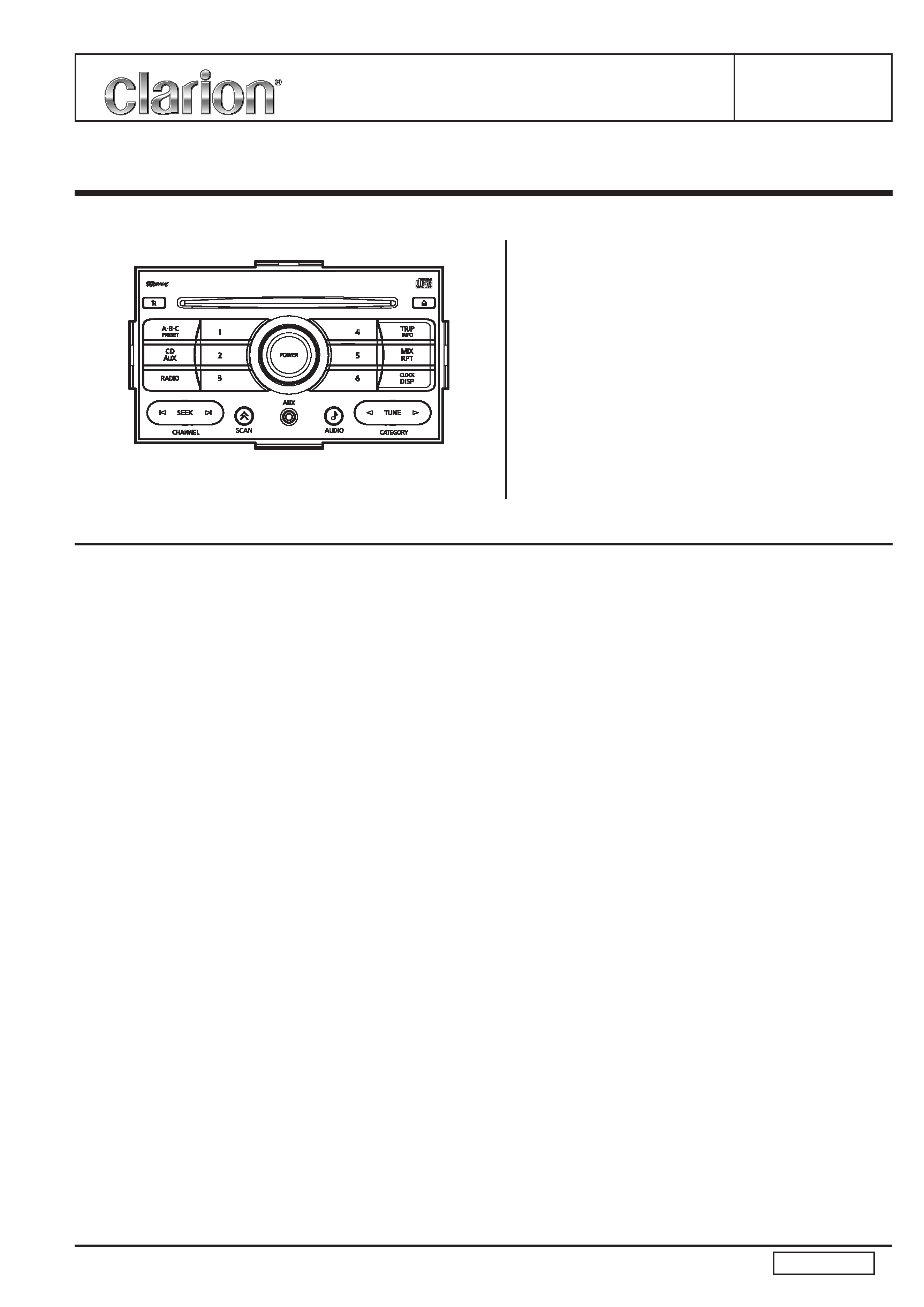
Top view of the unit

PN-2669M
- 3 -
ADJUSTMENT
Clock accuracy
adjustment
1. Set a universal timer to TP401(T-BASE), and adjust TC401 so that a reading of
the meter is 0+0.1/-0 sec./day.
Universal timer
EXPLANATION OF IC
051-6360-30
SAA7706H N20 Car radio Digital Signal Processor
Terminal Description
pin
1: VDACP
: positive reference voltage ADC1, ADC2,
ADC3 and level-ADC
pin
2: VDACN1
: ground reference voltage ADC1
pin
3: LEVEL
: LEVEL input pin; via this pin the level of the
FM signal or level of the AM signal is fed
to the DSP1; the level information is used in
the DSP1 for dynamic signal processing
pin
4: NAV_GND
: common mode reference input pin of the
navigation signal (pin AM_L/NAV)
pin
5: POM
: power-on mute of the QFSDAC; timing is
determined by an external capacitor
pin
6: RRV
: rear; right audio output of the QFSDAC
pin
7: AUX_L
: left channel of analog AUX input
pin
8: AUX_R
: right channel of analog AUX input
pin
9: RLV
: rear; left audio output of the QFSDAC
pin 10: VSS A2
: ground supply analog part of the QFSDAC
and SPDIF bitslicer
pin 11: VDD A2
: positive supply analog part of the QFSDAC
and SPDIF bitslicer
pin 12: VREFDA
: voltage reference of the analog part of QFS-
DAC
pin 13: FRV
: front; right audio output of the QFSDAC
pin 14: CD_R_GND
: common-mode reference input pin for analog
CD_R or TAPE_R in the event of separated
ground reference pins for left and right are
used
pin 15: DSP2_INOUT2 : flag input/output 2 of the DSP2-core (DSP2-
flag) I2C-bus configurable
pin 16: FLV
: front; left audio voltage output of the QFS-
DAC
pin 17: DSP2_INOUT1 : flag input/output 1 of the DSP2-core (DSP2-
flag) I2C-bus configurable
pin 18: DSP2_INOUT3 : flag input/output 3 of the DSP2-core (DSP2-
flag) I2C-bus configurable
pin 19: DSP2_INOUT4 : flag input/output 4 of the DSP2-core (DSP2-
flag) I2C-bus configurable
pin 20: LOOPO
: SYSCLK output (256fs)
pin 21: TP1
: for test purpose only; this pin may be left
open or connected to ground
pin 22: VDD D3V7
: positive supply (peripheral cells only)
pin 23: VSS D3V7
: ground supply (peripheral cells only)
pin 24: SPDIF2
: SPDIF input 2; can be selected instead of
SPDIF1 via I2C-bus bit
pin 25: SPDIF1
: SPDIF input 1; can be selected instead of
SPDIF2 via I2C-bus bit
pin 26: SYSFS
: system fs clock input
pin 27: CD_WS
: digital CD-source word select input; I2S-bus
or LSB-justified format
pin 28: CD_DATA
: digital CD-source left-right data input; I2S-
bus or LSB-justified format
pin 29: CD_CLK
: digital CD-source clock input I2S-bus or
LSB-justified format
pin 30: IIS_CLK
: clock output for external I2S-bus receiver; for
example headphone or subwoofer
pin 31: IIS_IN1
: data 1 input for external I2S-bus transmitter;
e.g. audio co-processor
pin 32: IIS_IN2
: data 2 input for external I2S-bus transmitter;
e.g. audio co-processor
pin 33: IIS_WS
: word select output for external I2S-bus re-
ceiver; for example headphone or subwoof-
er
pin 34: IIS_OUT1
: data 1 output for external I2S-bus receiver
or co-processor
pin 35: IIS_OUT2
: data 2 output for external I2S-bus receiver or
co-processor
pin 36: VDD D3V6
: positive supply (peripheral cells only)
pin 37: VSS D3V6
: ground supply (peripheral cells only)
pin 38: DSP1_IN1
: flag input 1 of the DSP1-core
pin 39: DSP1_IN2
: flag input 2 of the DSP1-core
pin 40: DSP1_OUT1
: flag output 1 of the DSP1-core
pin 41: DSP1_OUT2
: flag output 2 of the DSP1-core
pin 42: DSP_RESET
: general reset of chip (active LOW)
pin 43: RTCB
: asynchronous reset test control block; con-
nect to ground (internal pull-down)
pin 44: SHTCB
: shift clock test control block (internal pull-
down)
pin 45: TSCAN
: scan control active high (internal pull-down)
pin 46: VDD D3V5
: positive supply (peripheral cells only)
pin 47: VSS D3V5
: ground supply (peripheral cells only)
pin 48: VDD D3V1
: positive supply (core only)
pin 49: VSS D3V1
: ground supply (core only)
pin 50: VSS D3V2
: ground supply (core only)
pin 51: VDD D3V2
: positive supply (core only)
pin 52: VDD D3V3
: positive supply (core only)
pin 53: VSS D3V3
: ground supply (core only)
pin 54: VSS D3V4
: ground supply (core only)
pin 55: VDD D3V4
: positive supply (core only)
pin 56: A0
: slave sub-address I2C-bus selection or seri-
al data input test control block
pin 57: SCL
: serial clock input I2C-bus
pin 58: SDA
: serial data input/output I2C-bus
pin 59: RDS_CLOCK
: radio data system bit clock output or RDS
external clock input I2C-bus bit controlled
pin 60: RDS_DATA
: radio data system data output
pin 61: SEL_FR
: AD input selection switch to enable high
ohmic FM_MPX input at fast tuner search on
FM_RDS input
pin 62: VSS (OSC)
: ground supply (crystal oscillator only)
pin 63: OSC_IN
: crystal oscillator input
pin 64: OSC_OUT
: crystal oscillator output
pin 65: VDD (OSC)
: positive supply (crystal oscillator only)
pin 66: AM_FM R
: right channel AM/FM input; analog input pin
pin 67: AM_FM L
: left channel AM/FM input; analog input pin
pin 68: CD_R
: right channel of analog CD input
pin 69: CD_L
: left channel of analog CD input
pin 70: DVD_R
: right channel of analog DVD input
pin 71: PHONE
: common mode PHONE signal, analog input
pin
pin 72: DVD_L
: left channel of analog DVD input
pin 73: PHONE_GND
: common mode reference input pin of the
PHONE signal
pin 74: VDD A1
: positive supply analog (ADC1, ADC2, ADC3
and level-ADC only)
pin 75: VSS A1
: ground supply analog (ADC3 and level-ADC
only)
pin 76: VDACN2
: ground reference voltage (ADC2)
pin 77: DVD_GND
: common mode reference input pin for ana-
log DVD in the event of separated ground
reference pins used for DVD
pin 78: VREFAD
: common mode reference voltage ADC1,
ADC2, ADC3 and level-ADC
pin 79: FM_RDS
: FM RDS signal; analog input pin
pin 80: FM_MPX
: FM multiplex signal; analog input pin
Item
Procedure
Measuring instrument

PN-2669M
- 4 -
052-3208-00
M30843MW-M08GP
Audio CPU
Terminal Description
pin
1: AF MUTE
: O : Audio frequency signal muting.
pin
2: ILL PULSE
: IN : Illumination control signal input.
pin
3: EEP SD
:I/O: Serial data input/output for EEP-ROM.
pin
4: EEP CK
: O : EEP-ROM clock pulse out.
pin
5: BU DET
: IN : Backup detection signal input.
pin
6: BYTE
: IN : Data length selection(8bit/16bit).
pin
7: CN VSS
: IN : Connect to VSS via a resistor.
pin
8: ILL ON
: IN : Illumination ON signal input.
pin
9: SYS ON
: O : System ON signal output.
pin 10: RESET
: IN : Reset signal input.
pin 11: X out
: O : Crystal connection.
pin 12: GND
: - : Ground.
pin 13: X in
: IN : Crystal connection.
pin 14: VDD
: - : Positive voltage supply.
pin 15: NMI
: IN : Nonmaskable interrupt. Connect to VDD
via a resistor.
pin 16: ACC DET
: IN : ACC detection signal input.
pin 17: PLL DI
: IN : PLL serial data input.
pin 18: PLL DO
: O : PLL serial data output.
pin 19: TIME BASE
: IN : Time base pulse input.
pin 20: V-CAN RS
: O : V-CAN standby output.
pin 21: V-CAN RX
: IN : V-CAN serial data input.
pin 22: V-CAN TX
: O : V-CAN serial data output.
pin 23: P-IC STANDBY : O : Power IC Standby signal output.
pin 24: BEEP
: O : Beep out.
pin 25: NU
: - : Not in use.
pin 26: DIMMER
: O : PWM output.
pin 27: TUNER CK
: IN : Clock pulse input from the tuner pack.
pin 28: TUNER SD
:I/O: Serial data input/output to the tuner pack.
pin 29: NDS TX
: O : NDS serial data output to NDS-A/C.
pin 30: NDS RX
: IN : NDS serial data input from NDS-A/C.
pin 31: NDS REQ
: IN : The request pulse from NDS.
pin 32: NU
: - : Not in use.
pin 33: GS1 BUCK
: O : 1CD BUCK.
pin 34: GS1 CCE
: O : 1CD CCE.
pin 35: NU
: - : Not in use.
pin 36: NU
: - : Not in use.
pin 37: GS1 BUS
0
:I/O: 1CD
BUS
0.
pin 38: GS1 BUS
1
:I/O: 1CD
BUS
1.
pin 39: GS1 BUS
2
:I/O: 1CD
BUS
2.
pin 40: GS1 BUS
3
:I/O: 1CD
BUS
3.
pin 41: GS1 RESET
: O : 1CD Reset output.
pin 42: GS1 S STOP
: IN : 1CD S STOP.
pin 43: GS1 CHU SW
: IN : 1CD CHU SW.
pin 44: GS1 TR A
: IN : 1CD TR A.
pin 45: GS1 TR B
: IN : 1CD TR B.
pin 46: GS1 LD CONT : O : 1CD LD CONT.
pin 47: GS1 LD MUTE : O : 1CD LD MUTE.
pin 48: CD ON
: O : CD ON signal output.
pin 49: PWER DIAG
: IN : The diagnosis signal input for the power
IC.
pin 50: AM ON
: O : AM ON signal output.
pin 51: KEY STANDBY : O : Standby pulse output for the key scan IC.
pin 52: KEY CHIP SEL : O : Chip select signal output to the key scan
IC.
pin 53: COMMON CK
: IN : CCB Common clock.
pin 54: COMMON DO
: O : CCB Common data.
pin 55: KEY DI
: IN : Serial data input from the Key scan IC.
pin 56: VOL 2
: IN : Volume control pulse input from the rota-
ry encoder.
pin 57: VOL 1
: IN : Volume control pulse input from the rota-
ry encoder.
pin 58: NU
: - : Not in use.
pin 59: NU
: - : Not in use.
pin 60: VDD
: - : Positive voltage supply.
pin 61: POWER ON
: IN : Power ON signal input.
pin 62: GND
: - : Ground.
pin 63: NU
: - : Not in use.
pin 64: Mini Jack Det
: IN : Mini Jack connection detection.
pin 65: DISP C/D
: O : Display C/D output.
pin 66: DISP SI
: IN : Display serial data input.
pin 67: DISP SHT
: O : Display SHT output.
pin 68: DISP SO
: O : Display serial data output.
pin 69: DISP RESET
: O : Display reset signal output.
pin 70: DISP CS
: O : Display CS output.
pin 71: GS1 SBSY
: IN : 1CD sub code block synchronous signal
intput.
pin 72: DISP KEY REQ : IN : Display key request input.
pin 73: RDS CK
: IN : RDS clock pulse input.
pin 74: RDS DI
: IN : RDS data input.
pin 75: PLL CE
: O : PLL chip enable signal output.
pin 76: PLL CK
: O : PLL clock pulse output.
pin 77: NU
: - : Not in use.
pin 78: DSP RESET
: O : Reset signal output to the DSP IC.
pin 79: S METER
: IN : Input terminal of internal A/D converter to
monitor radio field strength.
pin 80: NU
: - : Not in use.
pin 81: NU
: - : Not in use.
pin 82: CLIP DET
: IN : Clipping detection for the audio power
amplifier.
pin 83: Power ON Mute : O : DSP power-on-mute output.
pin 84: FM ON
: O : FM ON signal output.
pin 85: TEMP
: IN : Input of the internal ADC for the temper-
ature sensor.
pin 86: TEL ON
: IN : Telephone ON signal input.
pin 87: NU
: - : Not in use.
pin 88: CD EJECT
: IN : CD eject switch signal input.
pin 89: NU
: - : Not in use.
pin 90: NU
: - : Not in use.
pin 91: NU
: - : Not in use.
pin 92: N REMO B
: IN : Steering wheel remote control signal input.
pin 93: N REMO A
: IN : Steering wheel remote control signal input.
pin 94: A GND
: - : Analog ground.
pin 95: ILL DC
: IN : The illumination voltage input.
pin 96: VREFI
: IN : Reference voltage input.
pin 97: A VCC
: - : Positive voltage supply for the internal
analog section.
pin 98: DSP PIC SCL
: O : I2C clock pulse output to the DSP and the
power IC.
pin 99: DSP/P-IC DO
: O : DSP/Power-IC serial data output.
pin100: ANT ON
: O : Antenna ON command output.
PN-2669M
- 5 -
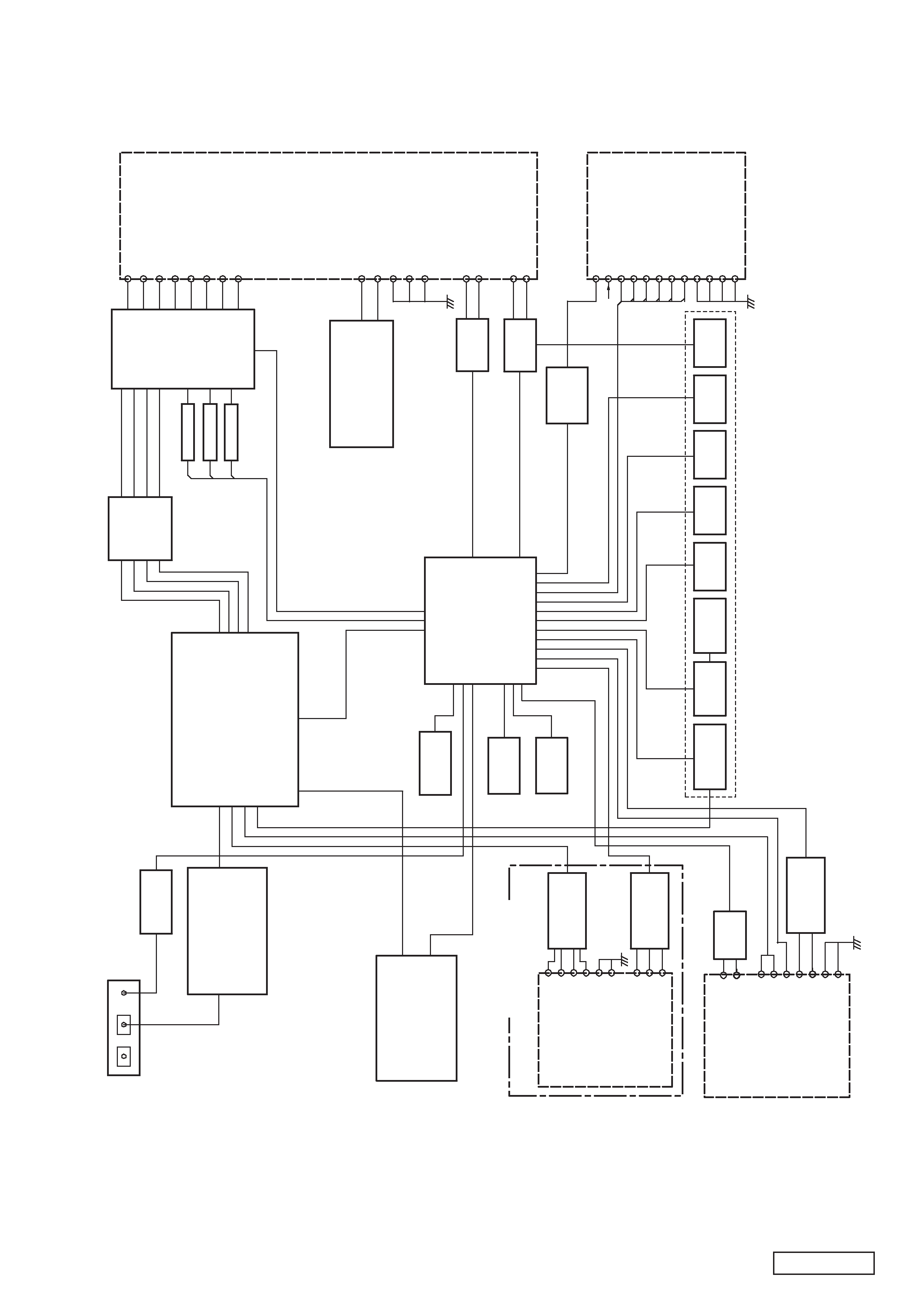
BLOCK DIAGRAM
SUB
MAIN
AM/FM-TUNER
POWER-IC
40W
x4
RESET
ANT101
BL101
GND
EEPROM
STBY
BEEP
BACK
UP
ACC
GND
SHIELD
GND
REQ
(CD
->
COMBI)
RX
(CD
->
COMBI)
TX
(COMBI
->
CD)
ANT-ON
STRG
SW
A
ILL-
ILL+
SHIELD
STRG
SW
B
STRG
SW
GND
GND
IC503
IC501
20K-LPF
PRE-AMP
IC301
DSP
N-BUS
AUDIO-IN
IC201
N-BUS
INTERFACE
TEL-IN+
J201(TEL/V-CAN)
TEL-IN-
TEL-ON
V-CAN+
TEL
SHIELD
V-CAN
SHIELD
V-CAN-
LED
GND
LED+
LED
GND
SO(SERIAL
OUTPUT)
RESET
SHT(SHIFT
CLOCK)
SI(SERIAL
OUTPUT)
C/D(COMMAND/DATA)
CS
VDD+
GND
AUX
MIN
JACK
KEY-IC
IC601
MAIN
VOL
CD-EJ
MUTE
ILL
J204(DISPLAY)
IC403
AUDIO-CPU
IC402
IC405
ANT-ON
PLL-IC
IC401
SYS+5V
ILL
CONT.
LIGHT+B
BACK
REMOTE
CONT.
POWER-SUPPLY
DIMMER
D-OUT
FM/AM
TEL
AUX
CD
FL
FR
RL
RR
N-BUS
LH
INPUT(-)
J820(N-BUS)
N-BUS
LH
INPUT(+)
N-BUS
RH
INPUT(-)
N-BUS
RH
INPUT(+)
N-BUS
DISP
KEY-
MATRIX
FR
LH(+)
J502(POWER/SP)
FR
LH(-)
RR
LH(+)
RR
LH(-)
FR
RH(+)
FR
RH(-)
RR
RH(+)
RR
RH(-)
CAN-
TRANCEVER
IC404
TEMP
TEMP+
TEMP-
For
PN-2669M-A
1CD
MECHANISM
CLIP
DET