PN-2529H-A
PN-2607H-A
- 1 -
Published by Service Dept.
Printed in Japan
Clarion Co., Ltd.
50 Kamitoda, Toda-shi, Saitama 335-8511 Japan
Service Dept.: 5-66 Azuma , Kitamoto-shi, Saitama 364-0007 Japan
Tel: +81-48-541-2335 / 2432 FAX: +81-48-541-2703
298-6052-00 Feb.2003 P
Service Manual
NISSAN Automobile Genuine
AM/FM Radio Stereo CD Deck
PN-2529H-A
(Genuine No. 28185 CA000)
PN-2607H-A
(Genuine No. 28185 CB700)
Model
DIFFERENCE FEATURE LIST
CLARION No.
Destination
PN-2529H-A
North America
PN-2607H-A
Other Countries
SPECIFICATIONS
Radio section
Tuning system:
PLL frequency synthesizer system
Receive range:
PN-2529H-A
AM 530kHz to 1,710kHz
FM 87.75Hz to 107.9MHz
Receive range:
PN-2607H-A
AM 530kHz to 1,620kHz
FM 87.5Hz to 107.9MHz
Intermediate frequency:
AM 450kHz
FM 10.7MHz
Quieting sensitivity:
AM Less than 38dBu(at 20dB S/N)
FM Less than 15dBu(at 30dB S/N)
Separation:
FM 22 +5/-7 dB(1kHz)
Auto tuning stop sensitivity:
AM 42 +6/-6 dBu(600kHz)
39 +6/-6 dBu(1000/1400kHz)
FM 32 +6/-6 dBu
CD section
Disc:
12cm,8cm Disc
Separation:
More than 50dB
S/N ratio:
More than 74dB
NAVI section (for PN-2529H-A)
NAVI Output Level:
580 +3/-3 dB
General
Load impedance:
4 ohm
Power output:
40W x 4
Power supply voltage: DC13.2V(10.8V to 15.6V)
Negative ground
Back-up consumption: Less than 0.5mA
Dimensions(mm):
180(W) x 106.4(H) x 148.4(D)
Weight:
Approx. 1.8kg
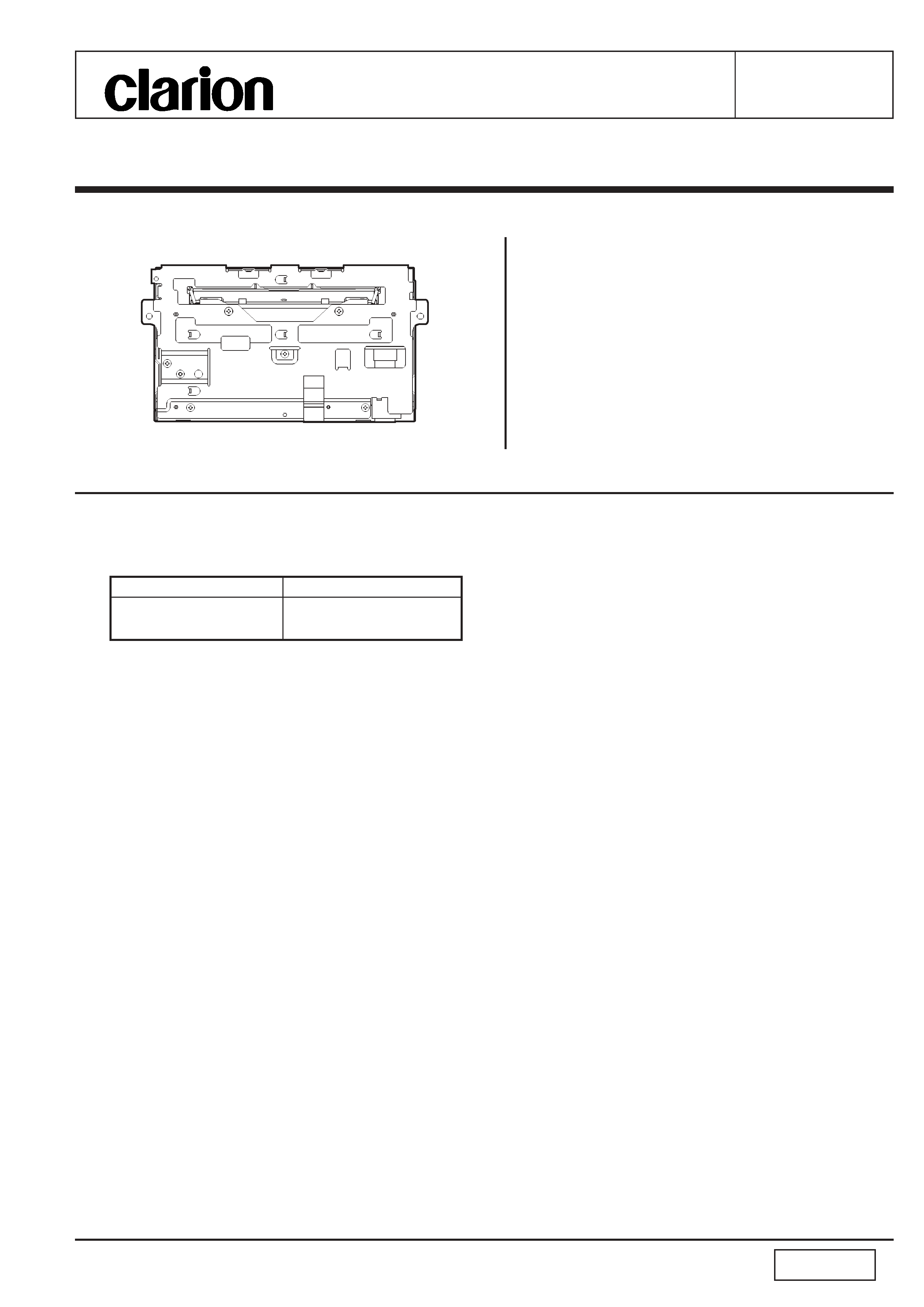
COMPONENTS
PN-2529H-A/PN-2607H-A
Main unit
-----------
1
NOTE
We cannot supply PWB with component parts in principle.
When a circuit on PWB has failure, please repair it by com-
ponent parts base. Parts which are not mentioned in ser-
vice manual are not supplied.
Specifications and design are subject to change without
notice for further improvement.
This unit is used the special adjustment jig for measuring.
Model
PN-2529H-A
PN-2607H-A
- 2 -
CAUTIONS
Use of controls,adjustment,or performance of
procedures other than those specified
herein,may result in hazardous radiation ex-
posure.
The compact disc player should not be ad-
justed or repaired by anyone except properly
qualified service personnel.
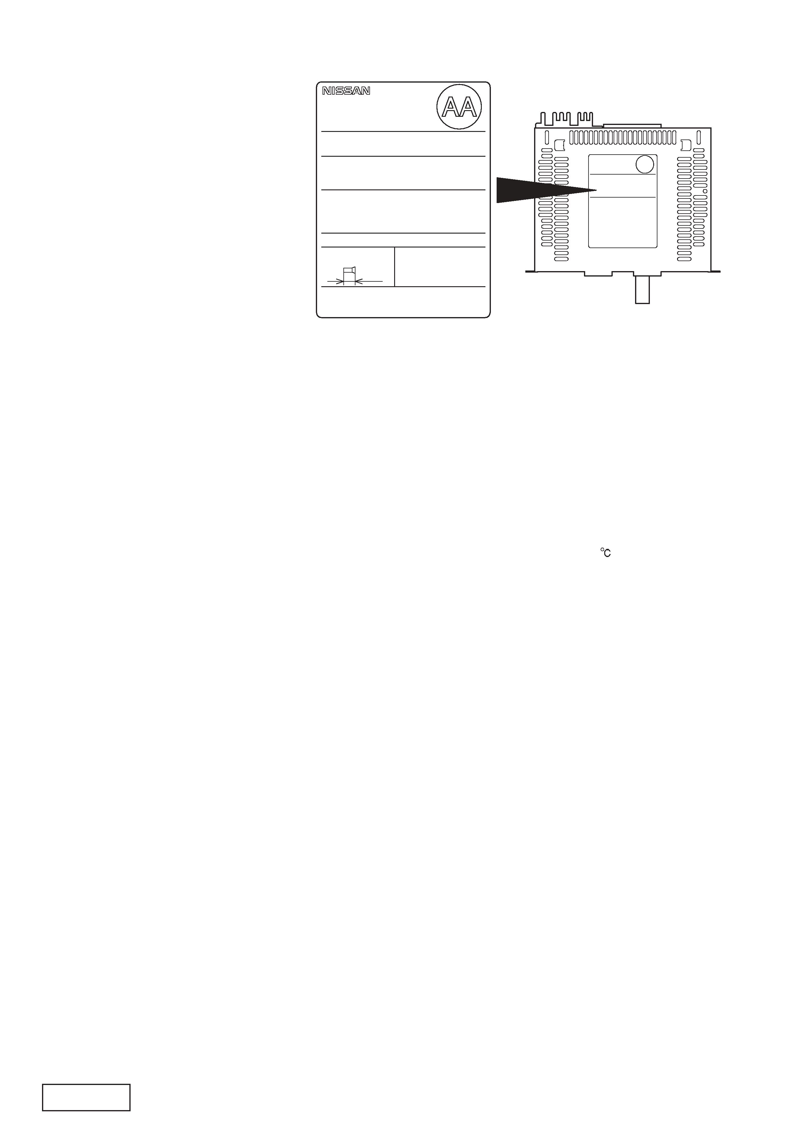
(for PN-2529H-A)
SER I A L
N O .
MA NUF A C T URE D
A M: 530k H z - 1710k H z
ISO
( FL AT MACHINE SCREW )
M5
PAR T
N o .
C l a r i o n
C o .,L td
F M: 87. 75MH z - 107. 9MH z
F R E QUE NCY RA NGE
T H I S
D EVI C E
C OMP L I ES
W I T H
PAR T
1 5
OF
T H E F C C
RUL E S .
OP E R A T I ON
I S
S UB J E CT
T O T H E F OL L OW I NG
T W O C ONDI T O I N S : ( 1 )
T HI S
D E V I CE
MA Y N OT
CA US E
HA RMF U L
I NT E R F E RE NCE , A ND( 2 )
T H I S DE V I CE
MU S T
A CCE P T
A N Y
I NT E R F E RE NCE RE CE I V E D , I NCL UDI NG
I N T E R F ER EN C E
T H AT
MA Y C AU SE U N D ESI R E D
OPER AT I ON .
T HI S
P RODUCT I ON COMP L I E S
W I T H DHHS RUL E S 2 1 CF R
SUBCHA PT ER J A P P L I CA BL E
A T DAT E OF M ANUF ACT URE .
MOUNT
S CRE W
5 0
KAM I T OD A, T OD A SH I , SAI T A MA
KEN , J APAN
8mm MAX
MO D E L
N O .
1 2 V (-)G R O U N D
P/N
28185 CA000
PN-2529H
286-9526-05
To engineers in charge of repair or
inspection of our products.
Before repair or inspection, make sure to follow the
instructions so that customers and Engineers in
charge of repair or inspection can avoid suffering
any risk or injury.
1. Use specified parts.
The system uses parts with special safety features against
fire and voltage. Use only parts with equivalent character-
istics when replacing them.
The use of unspecified parts shall be regarded as remod-
eling for which we shall not be liable. The onus of product
liability (PL) shall not be our responsibility in cases where
an accident or failure is as a result of unspecified parts
being used.
2. Place the parts and wiring back in their original positions
after replacement or re-wiring.
For proper circuit construction, use of insulation tubes,
bonding, gaps to PWB, etc, is involved. The wiring con-
nection and routing to the PWB are specially planned us-
ing clamps to keep away from heated and high voltage
parts. Ensure that they are placed back in their original
positions after repair or inspection.
If extended damage is caused due to negligence during
repair, the legal responsibility shall be with the repairing
company.
3. Check for safety after repair.
Check that the screws, parts and wires are put back se-
curely in their original position after repair. Ensure for safety
reasons there is no possibility of secondary ploblems
around the repaired spots.
If extended damage is caused due to negligence of repair,
the legal responsibility shall be with the repairing company.
4. Caution in removal and making wiring connection to the
parts for the automobile.
Disconnect the battery terminal after turning the ignition
key off. If wrong wiring connections are made with the bat-
tery connected, a short circuit and/or fire may occur. If ex-
tensive damage is caused due to negligence of repair, the
legal responsibility shall be with the repairing company.
5. Cautions regarding chips.
Do not reuse removed chips even when no abnormality is
observed in their appearance. Always replace them with
new ones. (The chip parts include resistors, capacitors,
diodes, transistors, etc). The negative pole of tantalum
capacitors is highly susceptible to heat, so use special care
when replacing them and check the operation afterwards.
6. Cautions in handling flexible PWB
Before working with a soldering iron, make sure that the
iron tip temperature is around 270 . Take care not to ap-
ply the iron tip repeatedly(more than three times)to the
same patterns. Also take care not to apply the tip with force.
7. Turn the unit OFF during disassembly and parts replace-
ment. Recheck all work before you apply power to the unit.
8. Cautions in checking that the optical pickup lights up.
The laser is focused on the disc reflection surface through
the lens of the optical pickup. When checking that the la-
ser optical diode lights up, keep your eyes more than 30cms
away from the lens. Prolonged viewing of the laser within
30cms may damage your eyesight.
9. Cautions in handling the optical pickup
The laser diode of the optical pickup can be damaged by
electrostatic charge caused by your clothes and body. Make
sure to avoid electrostatic charges on your clothes or body,
or discharge static electricity before handling the optical
pickup.
9-1. Laser diode
The laser diode terminals are shorted for transporta-
tion in order to prevent electrostatic damage. After
replacement, open the shorted circuit. When remov-
ing the pickup from the mechanism, short the termi-
nals by soldering them to prevent this damage.
9-2. Actuator
The actuator has a powerful magnetic circuit. If a
magnetic material is put close to it. Its characteris-
tics will change. Ensure that no foreign substances
enter through the ventilation slots in the cover.
9-3. Cleaning the lens
Dust on the optical lens affects performance. To
clean the lens, apply a small amount of isopropyl
alcohol to lens paper and wipe the lens gently.
Top view of main unit
PN-2529H-A
PN-2607H-A
- 3 -
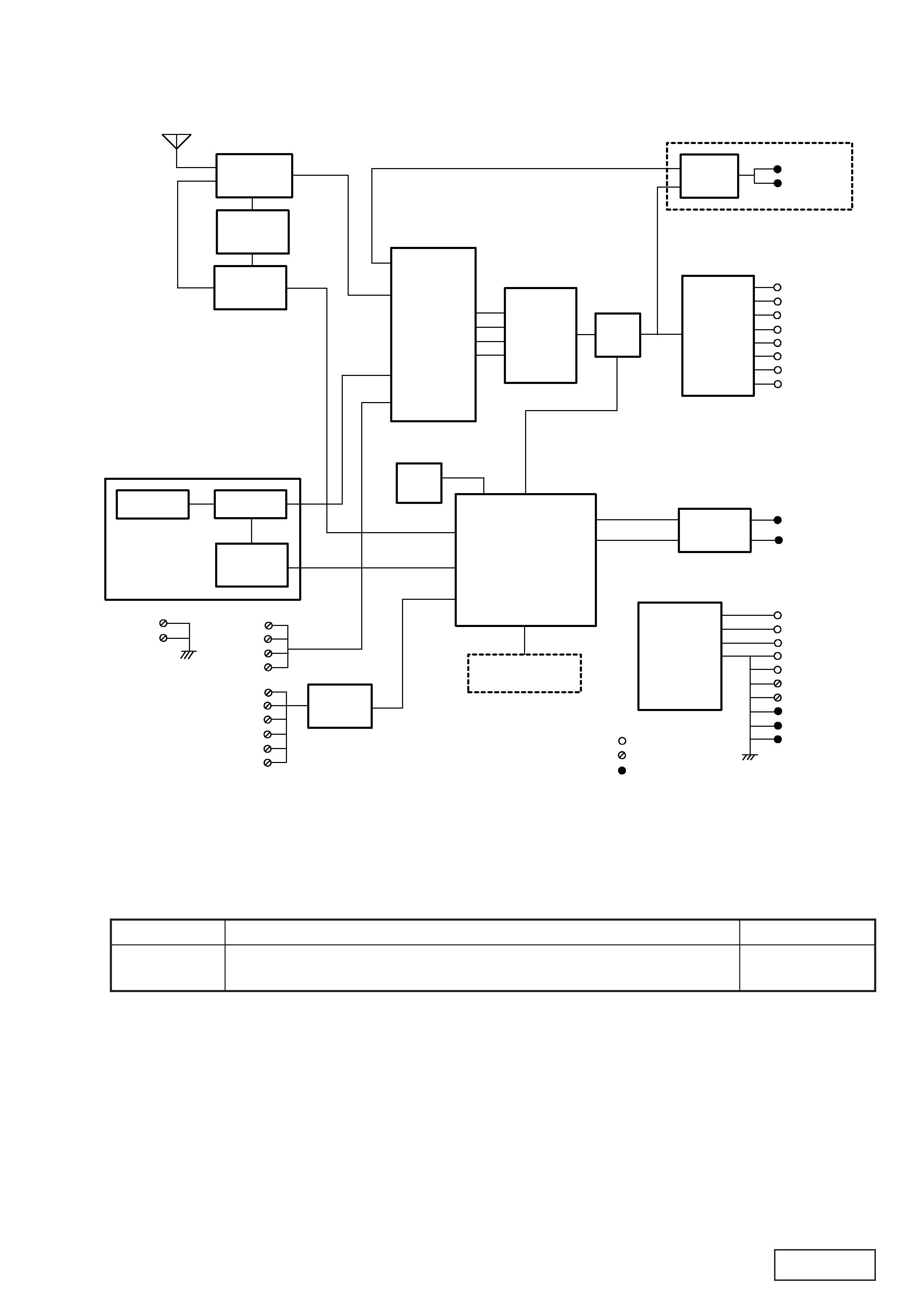
BLOCK DIAGRAM
ADJUSTMENT
Item
Procedure
Measuring
instrument
FM noise
convergence
1. Input the 98.1MHz/55dBu(1kHz,30%MOD)signal.(VOL1.4V=0dB)
2. Adjust the outputs to -22 +1/-1 dB by VR102 when the SG output is set -20dBu.
SSG
Milli-volt meter
(Only PN-2529H-A)
ANT
BL101
880-1917F
AM/FM TUNER
LPF
IC104
LC72191
PLL
CD MECHANISM
RF AMP
DSP/SSP/DAC
DRIVER
IC403
NJM4558
NAVI AMP
IC302
LC75412WH
ELECTRONIC
VOLUME
IC801,803
,804,806
NJM2060V
EQUALIZER
MUTE
IC808
TA8275
POWER IC
IC405
S-80933
RESET
IC404
M30624MGA
SYSTEM CONTROL
AUD-DCU
INTERFACE
POWER
SUPPLY
PANEL SW
A/C
INTERFACE
J601
J1002
J1001
CONNECTOR
NAVI-IN(-)
NAVI-IN(+)
FL SP(+)
FL SP(-)
FR SP(+)
FR SP(-)
RL SP(+)
RL SP(-)
RR SP(+)
RR SP(-)
TX(AUD-DCU)
ANT SIG
BACK UP
ACC
GND
GND
GND
DATA GND
DATA GND
GND
NAVI GND
CD L-IN(+)
GND
DATA GND
CD L-IN(-)
CD R-IN(+)
CD R-IN(-)
SOUCE-CHG
REQ
CHG-REQ2
CHG-CONT
RX
TX
RX(DCU-AUD)

PN-2529H-A
PN-2607H-A
- 4 -
052-3177-01
M30624MGA-179GP
System Controller
1.Terminal Description
pin
1: 1CD/6CD
: IN : The initial setting terminal. High = 1CD,
Low = 6CD.
pin
2: TAPE SEL
: IN : The initial setting terminal. High = without
tape.
pin
3: SCV SEL
: IN : The initial setting terminal. Low = without
SCV.
pin
4: NU
: - : Not in use.
pin
5: ES RETURN
: IN : The flexible PWB connection OK flag input.
pin
6: BYTE
: IN : The data length selection(8bit/16bit).
pin
7: CN VSS
: IN : Connect to VSS.
pin
8: TEST
: - : For the Test.
pin
9: NU
: - : Not in use.
pin 10: RESET
: IN : Reset signal input.
pin 11: X OUT
: O : Crystal connection.
pin 12: GND
: - : Ground.
pin 13: X IN
: IN : Crystal connection.
pin 14: VDD
: - : Positive supply voltage.
pin 15: NU
: - : Not in use.
pin 16: BU DET
: IN : Backup detection signal input.
pin 17: ACC IN
: IN : ACC ON flag input.
pin 18: TEL
: IN : The telephone interrupt pulse input.
pin 19: ILL ON
: IN : Illumination ON signal input.
pin 20: AMP ON
: O : Audio power amplifier ON signal output.
pin 21: SYS ON
: O : System ON signal output.
pin 22: NU
: - : Not in use.
pin 23: REAR MUTE
: O : The audio mute signal output for the rear
channels.
pin 24: NU
: - : Not in use.
pin 25: FRONT MUTE
: O : The audio mute signal output for the front
channels.
pin 26: 6-CD REQ
: IN : The request signal input from the 6CD-
Changer.
pin 27: 6-CD RX
: IN : The serial data input for 6CD-Changer.
pin 28: 6-CD TX
: O : The serial data output for 6CD-Changer.
pin 29: NDS FLASH TX : O : NDS serial data output for external A/C.
pin 30: NDS FLASH RX : O : NDS serial data input for external A/C.
pin 31: FLASH CLK
: O : Clock pulse output for flash memory.
pin 32: NU
: - : Not in use.
pin 33: DCU TX
: O : The serial data output to DCU.
pin 34: DCU RX
: IN : The serial data input from DCU.
pin 35: NDS CNT
: O : Low = A/C 1, High = A/C 2.
pin 36: NDS REQ 2
: IN : NDS request signal input.
pin 37: NDS REQ 1
: IN : NDS request signal input.
pin 38: SOURCE CHG : O : The signal source change signal output.
pin 39: FLASH EPM
: O : FLASH EPM.
pin 40: VOL EEP-R DO : O : Serial data output for Volume IC or EEP-
ROM.
pin 41: VOL EEP-R CK : O : Clock pulse output for Volume IC or EEP-
ROM.
pin 42: VOL CE
: O : The chip enable signal output to the vol-
ume IC.
pin 43: EEPROM CE
: O : The chip enable signal output to EEP-
ROM.
pin 44: FLASH CE
: IN : Chip enable signal input for flash memory.
pin 45: EEPROM DI
: IN : Serial data input from the EEP-ROM.
pin 46: NU
: - : Not in use.
pin 47: AUX ON
: IN : AUX ON signal input.
pin 48: COMBI ON
: O : Combi ON signal output.
pin 49: BUC 0
:I/O: CD IC Data input / output.
pin 50: BUC 1
:I/O: CD IC Data input / output.
pin 51: BUC 2
:I/O: CD IC Data input / output.
pin 52: BUC 3
:I/O: CD IC Data input / output.
pin 53: BUC CLOCK
: O : CD IC clock pulse output.
pin 54: CCE
: O : The chip enable signal output.
pin 55: CD RESET
: O : The reset pulse output to the CD IC.
pin 56: S STOP
: IN : Inside limit signal input from the CD mech-
anism.
pin 57: CHU SW
: IN : CD disc chucking signal input.
pin 58: TR A
: IN : Photo sensor signal input from the CD
mechanism.
pin 59: TR B
: IN : Photo sensor signal input from the CD
mechanism.
pin 60: VDD
: - : Positive supply voltage.
pin 61: LD CONT
:I/O: Loading motor control signal output.
pin 62: GND
: - : Ground.
pin 63: PLL CE
: O : The chip enable signal output to the PLL
IC.
pin 64: PLL CLK
: O : The clock pulse output to the PLL IC.
pin 65: PLL DO
: O : Serial data output to the PLL IC.
pin 66: PLL DI
: IN : Serial data input from the PLL IC.
pin 67: ST/TWEET
:I/O: Outputs "L" at AM 900kHz receiving. Inputs
"L" at FM stereo receiving.
pin 68: AMP MUTE
: O : Muting signal output to the Audio Power
Amplifier.
pin 69: MECH MUTE
: O : Muting signal output to the Tape mecha-
nism.
pin 70: RDS DI
: IN : RDS data input.
pin 71: RDS CLK
: IN : RDS clock pulse input.
pin 72: NU
: - : Not in use.
pin 73: TAPE IN
: IN : The tape in signal input.
pin 74: MODE BIT 1
: IN : The mode bit input from the tape mecha-
nism.
pin 75: MODE BIT 2
: IN : The mode bit input from the tape mecha-
nism.
pin 76: MODE BIT 3
: IN : The mode bit input from the tape mecha-
nism.
pin 77: REEL PULSE
: IN : Reel pulse input from the tape mechanism.
pin 78: APC SENSE
: O : APC gain control signal output.
pin 79: APC DET I
: IN : APC detected signal input.
pin 80: PWR MTR 1
: O : Power motor control signal output.
pin 81: PWR MTR 2
: O : Power motor control signal output.
pin 82: MAIN MTR
: O : Main motor control signal output.
pin 83: NR
: O : Noise reduction control.
pin 84: FWD/REV
: O : Forward/Reverse selection.
pin 85: LD MUTE
: O : Muting signal output to the CD mechanism.
pin 86: CD CONNECT
: IN : CD connection check signal input.
pin 87: 6-CD LOAD
: IN : The loading control signal input for 6CD-
Changer.
pin 88: TAPE EJECT
: IN : Tape eject signal input.
pin 89: 6-CD EJECT
: IN : The eject signal input for 6CD-Changer.
pin 90: NAVI MUTE
: O : Muting signal output to suppress the noise
without Navigation sound interrupting.
pin 91: NU
: - : Not in use.
pin 92: NU
: - : Not in use.
pin 93: NU
: - : Not in use.
pin 94: A VSS
: - : Analog ground.
pin 95: NU
: - : Not in use.
pin 96: Vref
: - : Reference voltage.
pin 97: A VCC
: - : Positive supply voltage for the internal an-
alog section.
pin 98: RBDS SEL
: IN : The initial setting terminal. High = without
RBDS.
pin 99: LCD RESET
: O : Reset pulse output to LCD.
pin100: BOSE AMP S
: IN : The initial setting terminal. High = BOSE
amplifier.
EXPLANATION OF IC
PN-2529H-A
PN-2607H-A
- 5 -
12
31
28
18
28
20
17
28
1-1
26
1-3
5
1-2
3
6
7
4
30
14
2
15
29
29
29
29
25
19
29
29
24
27
29
22
23
29
11
8
9
10
16
29
29
29
29
21
29
13
29
29
29
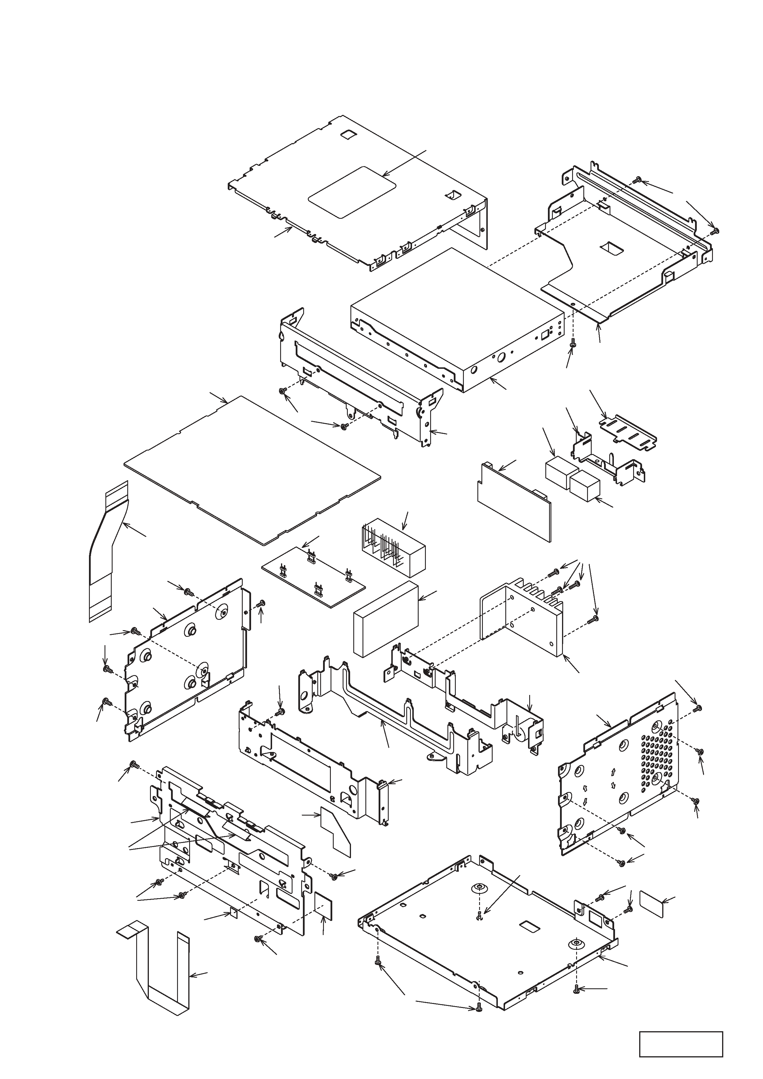
EXPLODED VIEW PARTS LIST
Main section