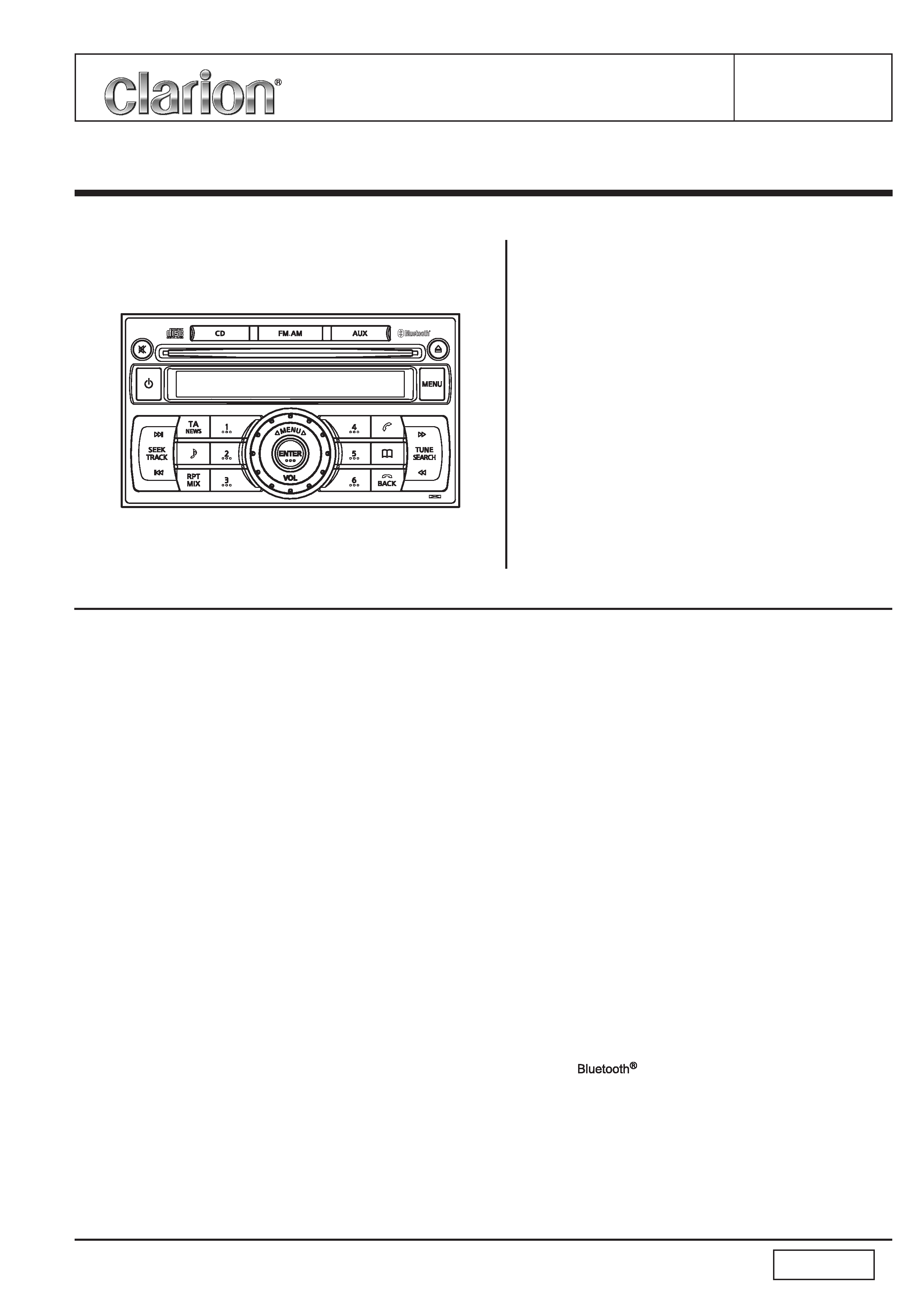
PN-3001P
PP-3001M
- 1 -
Service Manual
Published by Service Dept.
Printed in Japan
Clarion Co., Ltd.
7-2, Shintoshin, Chuo-ku, Saitama-shi, Saitama 330-0081 Japan
Service Dept.: 7-2, Shintoshin, Chuo-ku, Saitama-shi, Saitama 330-0081 Japan
Tel: +81-48-601-3705 FAX: +81-48-601-3804
298-6503-00 Oct.2007
Model
NISSAN Automobile Genuine
1CD LW/MW/FM/RDS Bluetooth
Combination
PN-3001P-A
(Genuine No.28185 9U10A)(ID No. CY02E)
(ES color : Black)
PP-3001M-A
(Genuine No.28185 BG10B)(ID No. CY01E)
(ES color : Brown)
PP-3001M-B
(Genuine No.28185 BG10A)(ID No. CY00E)
(ES color : Black)
SPECIFICATIONS
Radio section
Tuning system:
PLL Frequeency synthesizer sys-
tem
Receive range:
LW
153kHz to 279kHz
MW
531kHz to 1,602kHz
FM
87.5MHz to 108.0MHz
Intermediate frequency:
LW/MW/FM
10.7MHz
Quieting sensitivity:
LW
Less than 45dBu
(at 20dB S/N)
MW
Less than 32dBu
(at 20dB S/N)
FM
Less than 10dBu
(at 30dB S/N)
Separation:
FM
22+5/-7dB(1kHz)
S/N ratio:
LW
More than 40dB
MW
More than 40dB
FM
More than 50dB
Auto tuning stop sensitivity:
LW/MW
40+6/-6dBu
FM
22+6/-6dBu
CD section
Disc:
12cm disc
Separation:
More than 50dB
(IkHz, 20kHz L.P.F)
S/N ratio:
More than 74dB(JIS-A)
Distortion:
Less than 0.2%(20kHz L.P.F.)
General
Load impedance:
4ohm/CH
Power output:
40W x4
Power supply voltage: DC13.2V(10.8 to 15.6V)
Negative ground
Back-up consumption: Less than 0.5mA
Dimensions(mm):
178(W) x 100(H) x 163(D)
Weight:
1.6kg
NOTES
*
As for this model, the tuner of the DSP type is used.
When you exchange it due to the tuner pack(BL101;880-
2091M) trouble, it is necessary to adjust for S-meter etc.
Special JIG is necessary for an accurate adjustment. The
procedure document for the exclusive use jig is appended
to it.
*
This DSP IC SAF7730HV/N317(IC301) of Main PWB is
exposed die soldering pad type. It cannot remove in an
ordinary soldering iron.
Please use special removal JIG at the time of IC ex-
change
*
The
word mark and logos are owned by the
Bluetooth SIG, Inc. and any use of suchmarks by
CLARION CO.,LTD. is under license.
*
We cannot supply PWB with component parts in prin-
ciple. When a circuit on PWB has failure, please repair it
by component parts base. Parts which are not mentioned
in service manual are not supplied.
*
Specifications and design are subject to change without
notice for further improvement.
Model
Model
PN-3001P
PP-3001M
- 2 -
COMPONENT
PN-3001P-A, PP-3001M-A, PP-3001M-B
1.
Main unit
----------
1
2.
Radio pass card
----------
1
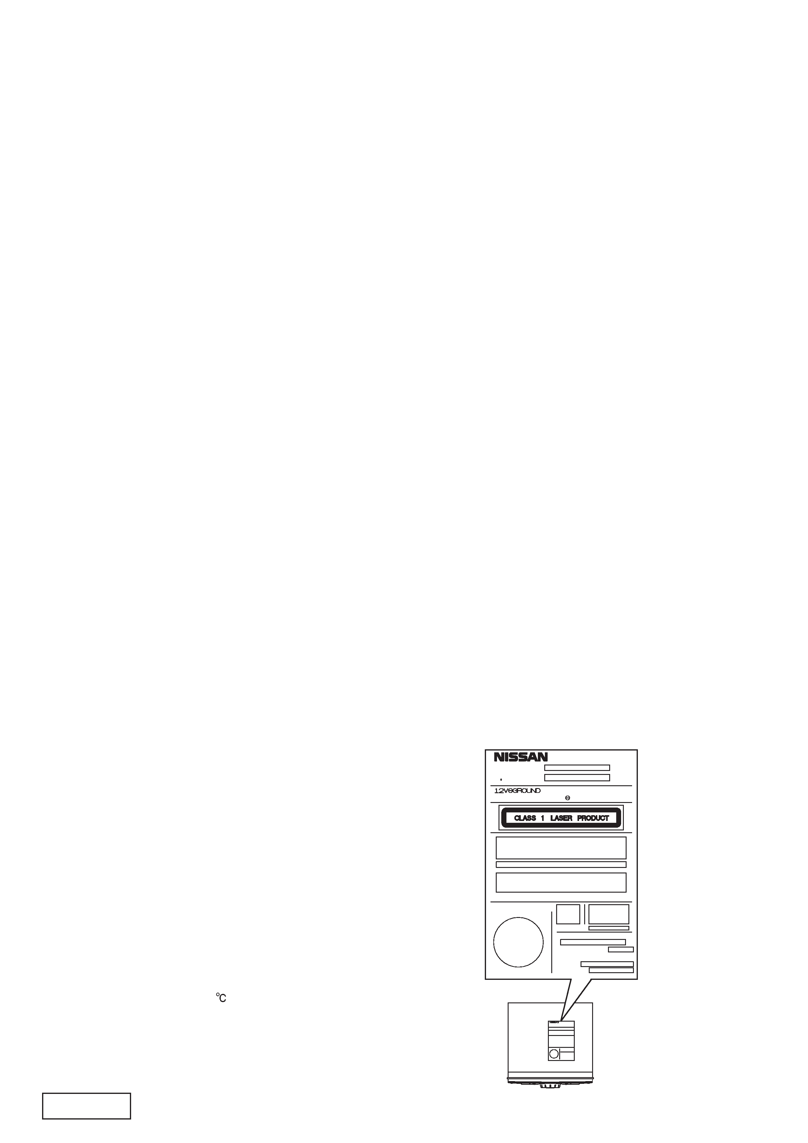
CAUTION
This appliance contains a laser system and is classified as
a "CLASS 1 LASER PRODUCT".To use this model
properly,read this Owner's Manual carefully and keep this
manual for your future reference.In case of any trouble with
this player,please contact your nearest "AUTHORIZED ser-
vice station".To prevent direct exposure to the laser beam,do
not to open the enclosure.
To engineers in charge of repair or
inspection of our products.
Before repair or inspection, make sure to follow the
instructions so that customers and Engineers in charge
of repair or inspection can avoid suffering any risk or
injury.
1. Use specified parts.
The system uses parts with special safety features against fire
and voltage. Use only parts with equivalent characteristics
when replacing them.
The use of unspecified parts shall be regarded as remodeling
for which we shall not be liable. The onus of product liability
(PL) shall not be our responsibility in cases where an accident
or failure is as a result of unspecified parts being used.
2. Place the parts and wiring back in their original positions after
replacement or re-wiring.
For proper circuit construction, use of insulation tubes, bond-
ing, gaps to PWB, etc, is involved. The wiring connection and
routing to the PWB are specially planned using clamps to keep
away from heated and high voltage parts. Ensure that they are
placed back in their original positions after repair or inspec-
tion.
If extended damage is caused due to negligence during re-
pair, the legal responsibility shall be with the repairing com-
pany.
3. Check for safety after repair.
Check that the screws, parts and wires are put back securely
in their original position after repair. Ensure for safety reasons
there is no possibility of secondary ploblems around the re-
paired spots.
If extended damage is caused due to negligence of repair, the
legal responsibility shall be with the repairing company.
4. Caution in removal and making wiring connection to the parts
for the automobile.
Disconnect the battery terminal after turning the ignition key
off. If wrong wiring connections are made with the battery con-
nected, a short circuit and/or fire may occur. If extensive dam-
age is caused due to negligence of repair, the legal responsi-
bility shall be with the repairing company.
5. Cautions in soldering
Please do not spread liquid flux in soldering.
Please do not wash the soldering point after soldering.
6. Cautions in soldering for chip capacitors
Please solder the chip capacitors after pre-heating for replace-
ment because they are very weak to heat.
Please do not heat the chip capacitors with a soldering iron
directly.
7. Cautions in handling for chip parts.
Do not reuse removed chips even when no abnormality is ob-
served in their appearance. Always replace them with new
ones. (The chip parts include resistors, capacitors, diodes, tran-
sistors, etc).
Please make an operation test after replacement.
8. Cautions in handling flexible PWB
Before working with a soldering iron, make sure that the iron
tip temperature is around 270
. Take care not to apply the
iron tip repeatedly(more than three times)to the same patterns.
Also take care not to apply the tip with force.
9. Turn the unit OFF during disassembly and parts replacement.
Recheck all work before you apply power to the unit.
10. Cautions in checking that the optical pickup lights up.
The laser is focused on the disc reflection surface through the
lens of the optical pickup. When checking that the laser opti-
cal diode lights up, keep your eyes more than 30cms away
from the lens. Prolonged viewing of the laser within 30cms
may damage your eyesight.
11. Cautions in handling the optical pickup
The laser diode of the optical pickup can be damaged by elec-
trostatic charge caused by your clothes and body. Make sure
to avoid electrostatic charges on your clothes or body, or dis-
charge static electricity before handling the optical pickup.
11-1. Laser diode
The laser diode terminals are shorted for transportation in or-
der to prevent electrostatic damage. After replacement, open
the shorted circuit. When removing the pickup from the mecha-
nism, short the terminals by soldering them to prevent this
damage.
11-2. Actuator
The actuator has a powerful magnetic circuit. If a magnetic
material is put close to it. Its characteristics will change. En-
sure that no foreign substances enter through the ventilation
slots in the cover.
11-3. Cleaning the lens
Dust on the optical lens affects performance.
To clean the lens, apply a small amount of isopropyl alcohol to
lens paper and wipe the lens gently.
NISSAN PART No.
N DE MODELE
MODEL NO.
TENSION D
UTILISATION 12V
AU CHASSIS
SERIAL No.
TYPE
DESIGN NOTE No.
PART NO.
MADE IN
Clarion co., Ltd
Bluetooth ID
276-
PN-3001P
PP-3001M
- 3 -
EXPLANATION OF IC
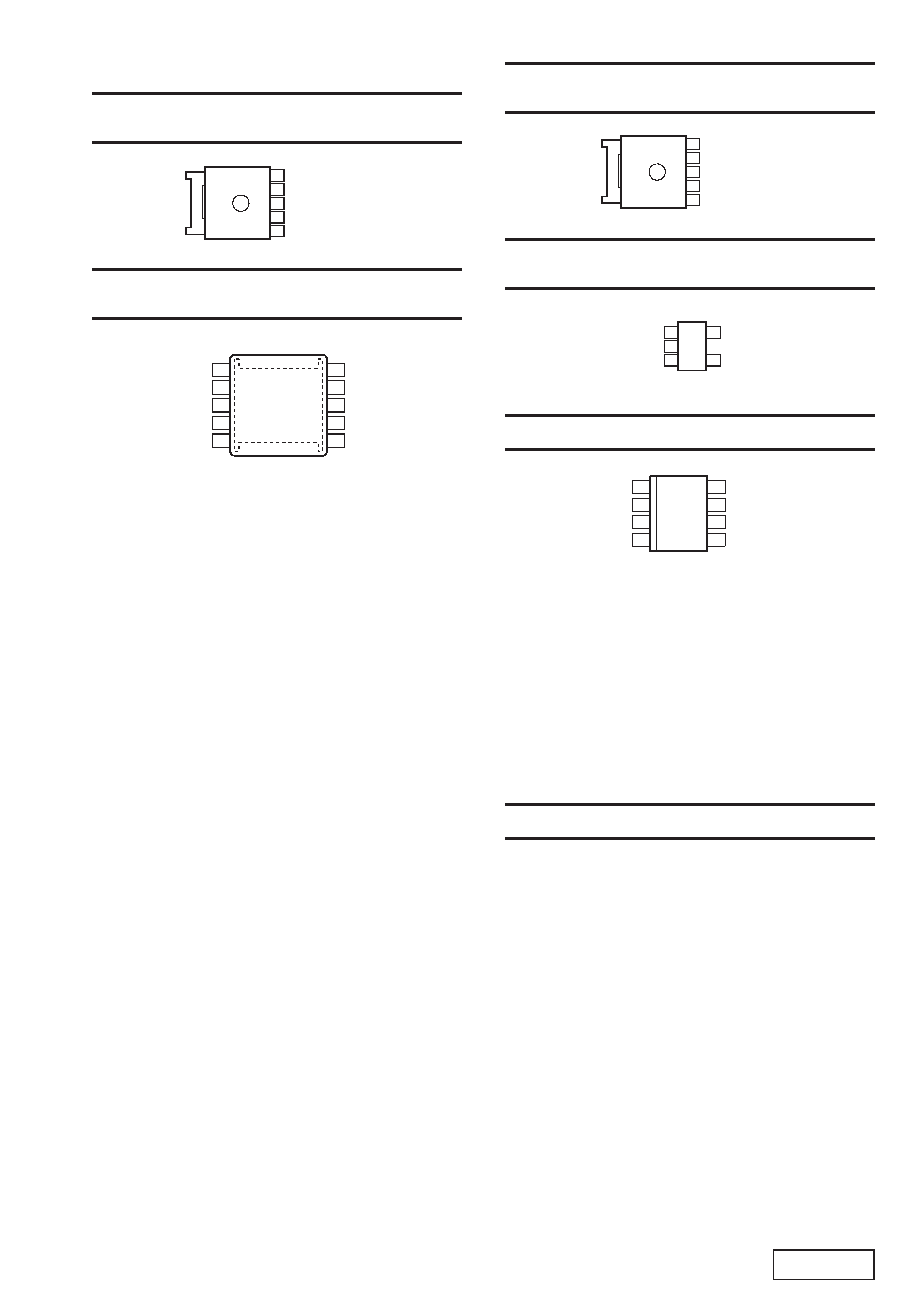
051-3396-90
NJM2386ADL3-33-TE1
Positive Voltage Regulator 3.3V
051-3517-90
impossible of exchange (LT3481EMSE#TRPBF)
Step-Down Switching Regulator
Terminal Description
BD (Pin 1):
This pin connects to the anode of the boost Schottky diode.
BOOST (Pin 2):
This pin is used to provide a drive voltage, higher than the input
voltage, to the internal bipolar NPN power switch.
SW (Pin 3):
The SW pin is the output of the internal power switch. Connect this
pin to the inductor, catch diode and boost capacitor.
VIN (Pin 4):
The VIN pin supplies current to the LT3481's internal regulator and
to the internal power switch. This pin must be locally bypassed.
RUN/SS (Pin 5):
The RUN/SS pin is used to put the LT3481 in shutdown mode. Tie
to ground to shut down the LT3481. Tie to 2.3V or more for nor-
mal operation. If the shutdown feature is not used, tie this pin to
the VIN pin.
PG (Pin 6):
The PG pin is the open collector output of an internal comparator.
PG remains low until the FB pin is within 10% of the final regula-
tion voltage. PG output is valid when VIN is above 3.5V and RUN/
SS is high.
BIAS (Pin 7):
The BIAS pin supplies the current to the LT3481's internal regula-
tor. Tie this pin to the lowest available voltage source above 3V
(typically VOUT). This architecture increases efficiency especially
when the input voltage is much higher than the output.
FB (Pin 8):
The LT3481 regulates the FB pin to 1.265V. Connect the feedback
resistor divider tap to this pin.
VC (Pin 9):
The VC pin is the output of the internal error amplifier. The volt-
age on this pin controls the peak switch current. Tie an RC net-
work from this pin to ground to compensate the control loop.
RT (Pin 10):
Oscillator Resistor Input. Connecting a resistor to ground from this
pin sets the switching frequency.
Exposed Pad (Pin 11):
Ground. The Exposed Pad must be soldered to PCB.
051-3518-90
NJM2846DL3-33-TE1
Positive Voltage Regurator 3.3V
051-3519-90
NJU7771F05-TE2
Positive Voltage Regurator 5.0V
051-9425-80
S-24CS64A0I-J8T1G
EEP-ROM
Terminal Description
pin
1: A
0
: IN : Address input.
pin
2: A
1
: IN : Address input.
pin
3: A
2
: IN : Address input.
pin
4: GND
: - : Ground.
pin
5: S DA
:I/O: Serial data input/output.
pin
6: S CK
: IN : Serial clock pulse input.
pin
7: Write Protect
: IN : Write protect signal input.
H = protect ON.
pin
8: VCC
: - : Positive voltage supply.
052-0320-00
M30876FJBGP
System Contoller
[ Note ] The program is not written in this IC. Therefore, you need to
write a program in this IC with the part exchange.
Terminal Description for PN-3001
pin
1: NU
: IN : Not in use.
pin
2: Speed Pulse
: IN : Speed pulse input.
pin
3: IMMOBI TX
: O : Serial data output for IMMOBI.
pin
4: IMMOBI RX
: IN : Serial data input for IMMOBI.
pin
5: BU DET
: IN : Backup detection signal input.
pin
6: GND
: - : Ground.
pin
7: CN VSS
: IN : Connect to VSS via a resistor.
pin
8: ILL ON
: IN : Illumination ON signal input.
pin
9: SYS ON
: O : System ON signal output.
pin 10: RESET
: IN : Reset signal input.
pin 11: X out
: O : Crystal connection.
pin 12: VSS
: - : Negative voltage supply.
pin 13: X in
: IN : Crystal connection.
pin 14: VDD
: - : Positive voltage supply.
pin 15: NMI
: IN : Nonmaskable interrupt. Connect to VDD
via a resistor.
pin 16: ACC IN
: IN : ACC ON flag input.
pin 17: PLL DO
: O : PLL serial data output.
5
4
3
2
1
Ground
N.C.
Power Outut
Control in, H = ON.
VCC
3
RT
VC
FB
BIAS
PG
10
9
8
7
6
BD
BOOST
SW
VIN
RUN/SS
1
2
3
4
5
TOP VIEW
11
5
4
3
2
1
N.C
Power Outut
Ground
VCC
Control in, H = ON.
3
1
2
3
5
4
Vin
Vout
Control (H= On)
Ground
N.C.
VCC
WP
SCL
SDA
8
7
6
5
A 0
A 1
A 2
GND
1
2
3
4

PN-3001P
PP-3001M
- 4 -
pin 18: NU
: - : Not in use.
pin 19: B/T CTS
: IN : BT module UART flow control.
pin 20: B/T RX
: IN : BT module UART data input.
pin 21: TIME BASE
: IN : Time base pulse input.
pin 22: B/T TX
: O : BT module UART data output.
pin 23: PLL CE
: O : PLL chip enable signal output.
pin 24: DIMMER
: O : DIMMER output.
pin 25: PLL CK
: O : PLL clock pulse output.
pin 26: NU
: - : Not in use.
pin 27: DSP SCL
: O : Clock pulse output to the DSP IC.
pin 28: DSP SDA
:I/O: Serial data input/output for the digital sig-
nal processor.
pin 29: NDS/BT TX
: O : Serial data output for NDS and Blue-tooth.
pin 30: NDS/BT RX
: IN : Serial data input for NDS and Blue-tooth.
pin 31: NDS REQ 1
: IN : NDS request signal input.
pin 32: 1CD SLOT
: - : 1CD SLOT signal output.
pin 33: NU
: - : Not in use.
pin 34: NU
: - : Not in use.
pin 35: BUS CLOCK
: O : CD IC clock pulse output.
pin 36: CCE
: O : Chip enable signal output.
pin 37: BUS 0
:I/O: CD IC Data input / output.
pin 38: BUS 1
:I/O: CD IC Data input / output.
pin 39: BUS 2
:I/O: CD IC Data input / output.
pin 40: BUS 3
:I/O: CD IC Data input / output.
pin 41: RESET
: O : Reset signal output.
pin 42: S STOP
: IN : Inside limit signal input from the CD mech-
anism.
pin 43: CHU SW
: IN : CD disc chucking signal input.
pin 44: TR A
: IN : Photo sensor signal input from the CD
mechanism.
pin 45: TR B
: IN : Photo sensor signal input from the CD
mechanism.
pin 46: LD CONT
: O : Loading signal output.
pin 47: LD MUTE
: O : Muting signal output to the CD mecha-
nism.
pin 48: CD ON
: O : CD ON signal output.
pin 49: NU
: - : Not in use.
pin 50: Power IC Stndb : O : The standby signal output to the power IC.
pin 51: LCD DO
: O : Serial data output to the LCD controller.
pin 52: LCD CK
: O : Clock pulse output to the LCD driver.
pin 53: LCD DI
: IN : Serial data input from the LCD driver.
pin 54: LCD CE
: O : Chip enable signal output to the LCD driv-
er.
pin 55: LCD RST
: O : Reset pulse output to the LCD driver.
pin 56: VOL 3
: IN : Volume control pulse input from the rota-
ry encoder.
pin 57: VOL 2
: IN : Volume control pulse input from the rota-
ry encoder.
pin 58: VOL 1
: IN : Volume control pulse input from the rota-
ry encoder.
pin 59: FAN ON
: O : The fan on signal output.
pin 60: VDD
: - : Positive voltage supply.
pin 61: POWER ON
: IN : Power ON signal input.
pin 62: GND
: - : Ground.
pin 63: BT-TEST-MODE : O : BT test mode signal output.
pin 64: AUX ON
: IN : AUX ON signal input.
pin 65: DIAG INPUT
: IN : Diagnosis signal input from the audio pow-
er IC.
pin 66: B/T RTS
: O : BT module UART flow control. AUX con-
nection detection.
pin 67: B/T TEST
: O : BT module test.
pin 68: B/T BOOTE
: O : BT module rewrite.
pin 69: B/T RESET P
: O : BT module reset.
pin 70: NU
: - : Not in use.
pin 71: GS1 SBSY
: IN : 1CD sub code block synchronous signal
intput.
pin 72: RDS CL 1
: IN : RDS 1 serial clock output.
pin 73: RDS DA 1
: IN : RDS 1 serial data input.
pin 74: NU
: - : Not in use.
pin 75: P IC MUTE
: O : Muting-command output for the audio pow-
er IC.
pin 76: MH MUTE
: O : Muting-command output for RDS and
DSP.
pin 77: M AGC BUFF
: IN : DSP Keyed AGC detection.
pin 78: DSP RESET
: O : Reset signal output to the DSP IC.
pin 79: MT S METER
: IN : Input of internal A/D converter to monitor
the radio field strength for the Main-tun-
er.
pin 80: MT SAMPLE
: IN : Main-tuner sample input.
pin 81: MT HOLD
: IN : AF-hold-signal input from the Main-tuner.
And S-hold signal input from the DSP.
pin 82: EQ 1
: IN : The equalizer setting input.
pin 83: EQ 2
: IN : The equalizer setting input.
pin 84: EQ 3
: IN : The equalizer setting input.
pin 85: EQ 4
: IN : The equalizer setting input.
pin 86: NU
: IN : Not in use.
pin 87: CD EJECT
: IN : CD eject signal input.
pin 88: LOAD
: IN : LOAD signal input.
pin 89: NU
: - : Not in use.
pin 90: NU
: - : Not in use.
pin 91: INI KEY
: IN : Initializing command input.
pin 92: REMO A
: IN : Steering wheel remote controller signal
input.
pin 93: REMO B
: IN : Steering wheel remote controller signal
input.
pin 94: A GND
: - : Analog ground.
pin 95: NU
: - : Not in use.
pin 96: VREF
: IN : Reference voltage input.
pin 97: A VCC
: - : Positive voltage supply for the internal
analog section.
pin 98: MT SCL
: IN : Main-tuner control clock pulse.
pin 99: MT SDA
:I/O: Serial data input/output for the Main-tun-
er.
pin100: DSP PAUSE
: IN : DSP automatic mute control. L = mute on.
PN-3001P
PP-3001M
- 5 -
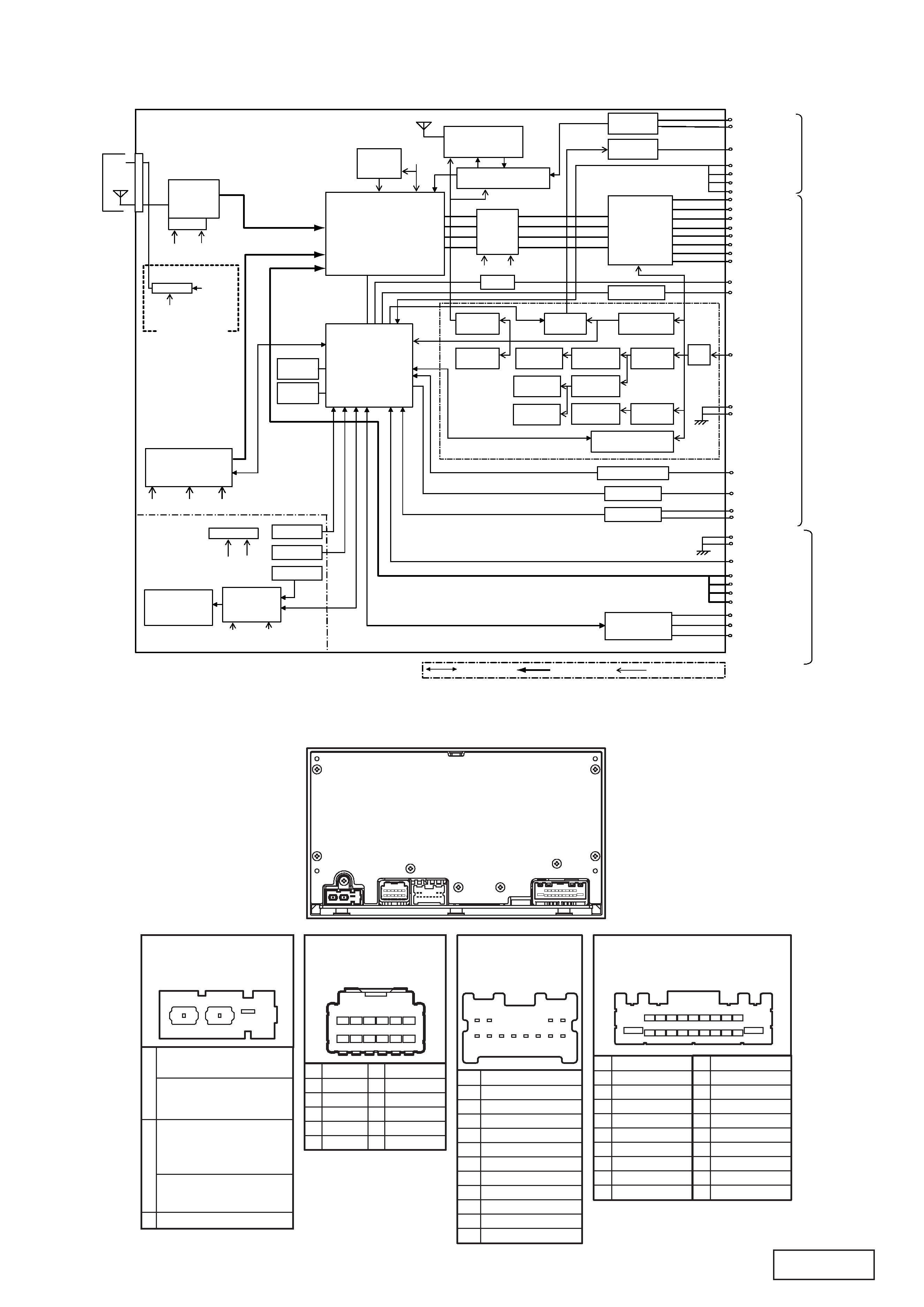
BLOCK DIAGRAM
Rear view of the unit
ANT101
J201
J502
J204
ANT101
ANT Connector
(GT13)
C
B
A
11
12
13
14
15
16
17
18
19
20
FRONT-RH(+)
FRONT-RH(-)
REAR-RH(+)
REAR-RH(-)
STRG GND
STRG SW B
IMMOBILIZER
SPEED SIGNAL
BACK UP
GND
MIC SIGNAL
N.C.
7
8
9
10
11
12
N.C.
N.C.
MIC GND
MIC VCC
1
N.C.
EQ1
EQ2
EQ3
2
3
4
5
6
EQ4
N.C.
V01 CD-LH(-)
V02
V03
V04
CD-LH(+)
CD-RH(-)
CD-RH(+)
V05
V06
V07
V08
V09
V10
V11
V12
EARTH
SHIELD-EARTH
N.C.
N.C.
AUX-ON
1
N.C.
2
3
4
FRONT-LH(+)
FRONT-LH(-)
REAR-LH(+)
5
6
7
8
9
10
REAR-LH(-)
STRG SW A
ACC
N.C.
ILLUMI (+)
N.C.
1
2
34
5
6
78
9 10 11 12
J201
NAVI Connector
(TH12 HW)
J204
NDS Connector
(A12 MW)
V02 V04
V10 V12
V01 V03 V05 V06 V07 V08 V09 V11
1
2 34 5
67 89
19
10 11 12 13 14 15 16 17 18
20
J502
Main Connector
(TH18 )
ANTENNA ON
( PN-3001P-A )
N.C.
( PP-3001M-A )
( PP-3001M-B )
ACTIVE ANT
: USED ANTENNA BOOST
AMP TYPE
( PN-3001P-A )
A
B
C N.C.
PASSIVE ANT
( PP-3001M-A )
( PP-3001M-B )
CHG - REQ1
CHG - COMBI (RXD)
COMBI - CHG (TXD)
CONNECTOR LAYOUT
DSP
AUDIO-CPU
M30876FJBGP
IC402
POWER IC
40W
4CH
4
TA8275
IC503
EEPROM
IC406
MIC+B
Q219,Q220
CD-EJ
GUIDE ILL
Digital
MIC SIGNAL
ACC-DET Q520
SAF7730
IC301
ILL+
B/U
FIL
VDD 5V
REG IC505
SYS 12V
Q516,517
SYS 5V
Q518,519
POWER
-SUPPLY
LCD
1/8DUTY
5 x 7 DOT x 13
LCD DRIVER
LC75816
IC801
BL+9V,DIMMER
Q506,507,509
KEY
1/2SYS 9V
ILL-
IMMOBI I/F
SSV
VOLUME
BASS
TREBLE
BALANCE
FADER
EQ
RDS
AM NC
SOUND FOUCUS
SYS-1.8V
REG
Q301
DSP-3.3V
DSP-3.3V
IC504
SYS5V
SYS9V
CD 8V
IC204
SYS 9V
Q515
TUNER 9V
Q109
TUNER 5V
IC104
CODEC-IC AK2301A
IC101
BLUETOOTH
UGZZ5
IC901
MIC AUDIO
I/F
MIC GND
CERAMIC-ANT
ANT902
BT 3.3V
IC502
RESET
IC404
20K LPF
IC501
1/2SYS 9V
SYS 9V
SWITCH PWB
CD
MECHANISM
FR-L +
FR-L -
FR-R +
FR-R -
RR-L +
RR-L -
RR-R +
RR-R -
SPEED SIGNAL
IMMOBILIZER
BACK UP
GND
STRG GND
REMOCOM
ILL
ACC
ILLUMI +
STRG SW A
STRG SW B
MIC VCC
EARTH
SHIELD-EARTH
AUX-ON
CD-LH(-)
CD-LH(+)
CD-RH(-)
CD-RH(+)
J204
NDS Connector
(A12 MW)
J502
Main Connector
(TH18 )
J201
NAVI Connector
(TH12 HW)
POWER-SUPPLY
CONTROL
AUDIO-SIG
IF
TUNER
AM/FM
ANT-ON
+B
ANT
-ON
ANT
ANT101
GT13
E2 PROM
SYS5V
TUNER9V
TUNER5V
Q110,111
( PN-3001P-A )
BL101
EQ1
EQ2
EQ3
EQ4
1CD 8V
1CD 3.3V
1CD 5V
MUTE
N-BUS/AUX-SIG
CD 3.3V
IC203
CD 5V
Q217
N-BUS I/F
Q208 - Q212
CHG-REQ1
CHG-COMBI(RXD)
COMBI-CHG(TXD)