- 1 -
PN-2165M
Published by Service Dept.
Printed in Japan
Clarion Co., Ltd.
Export Division - 22-3, Shibuya 2-chome, Shibuyaku, Tokyo, 150-8335 Japan
Tel: 03-3400-1121
Service Dept.- 50 kamitoda,Toda-shi,Saitama,335-8511 Japan Tel: 048-443-1111
FAX:048-433-6996
298-5779-00 Dec.1999 P
Service Manual
Model
Model
Model
NISSAN Automobile Genuine
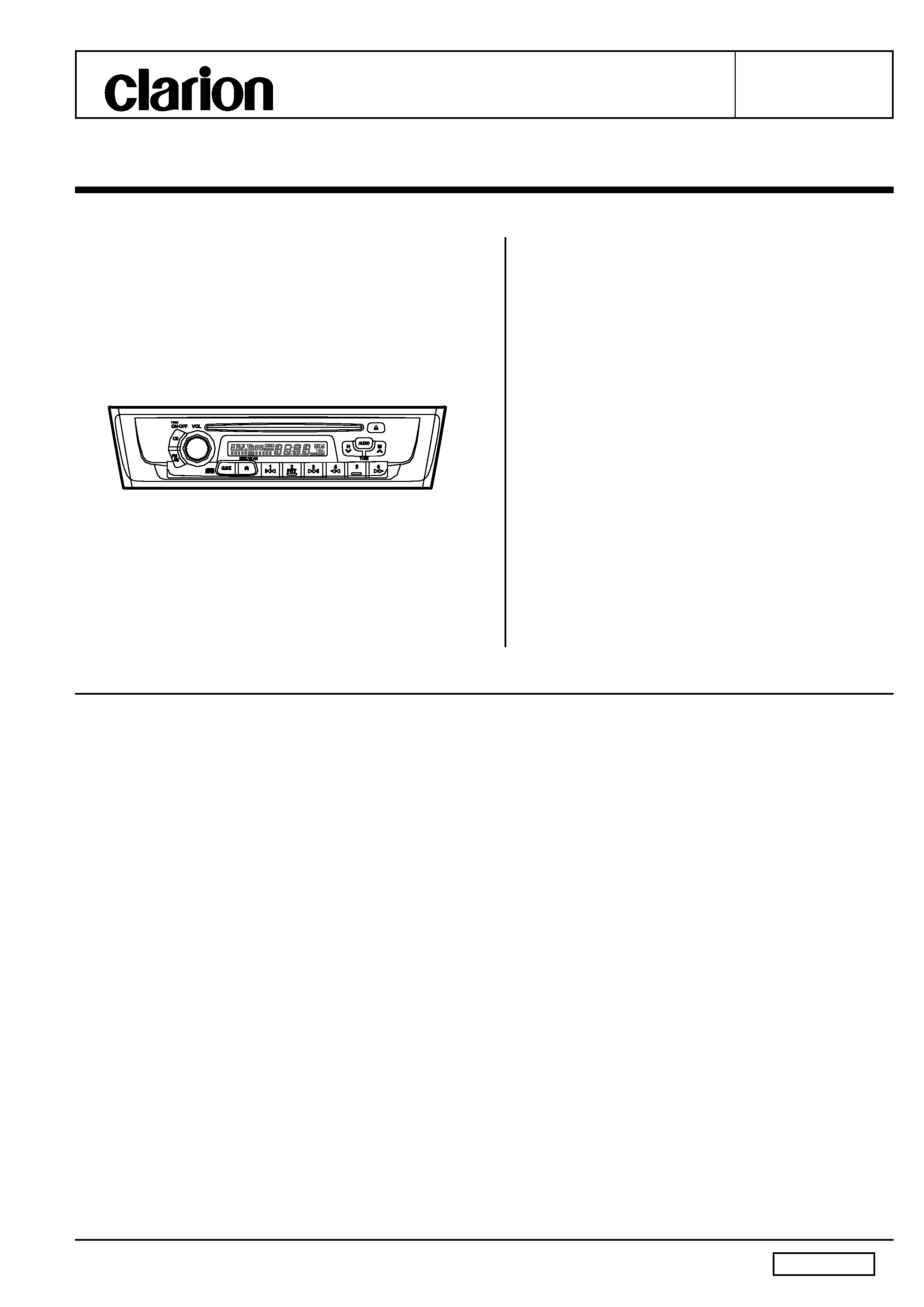
AM/FM Radio CD Stereo
(ID No. CY018 / Black Escutcheon)
(ID No. CY038 / Brown Escutcheon)
(ID No. CY068 / Gray Escutcheon)
·¡
SPECIFICATIONS
Radio section
Tuning system:
PLL Frequency synthesizer system
Receive range:
AM
530kHz to 1,710kHz
FM
87.9MHz to 107.9MHz
Intermediate frequency:
AM
450·}3kHz
FM
10.7·}0.2MHz
Quieting sensitivity:
AM
Less than 32dBÊ(at 20dB S/N)
FM
Less than 10dBÊ(at 30dB S/N)
Separation:
FM
More than 20dB(at 1kHz)
Auto tuning stop sensitivity:
AM
36·}6dBÊ
FM
25·}6dBÊ
General
Output power:
30W·~4
Power supply voltage: DC14.4V(10.8V to 15.6V)
Negative ground
Back-up consumption: Less than 3mA
Dimensions(mm):
264.2(W)·~63.6(H)·~171.9(D)
Weight:
1.7kg
·¦
Specifications and design are subject to change without
notice for further improvement.
·¡
COMPONENT
PN-2165M-A / PN-2165M-B / PN-2165M-C
Main unit
·|·|·|·|·|
1
·¡
NOTE
We cannot supply PWB with component parts in principle.
When a circuit on PWB has failure , please repair it by com-
ponent parts base. Parts which are not mentioned in ser-
vice manual are not supplied.
PN-2165M-B
PN-2165M-C
PN-2165M-A
(Genuine No. 28185 5M000)
(Genuine No. 28185 5M010)
(Genuine No. 28185 5M020)
CD section
Disc:
12cm,8cm Disc
Frequency response:
17Hz to 20kHz(·}3dB)
Separation:
More than 50dB(1kHz,0.5W)
S/N ratio:
More than 74dB(1kHz,5W)
Distortion:
Less than 0.4%(1kHz,0.5W)

- 2 -
PN-2165M
To engineers in charge of repair or
inspection of our products.
Before repair or inspection, make sure to follow
the instructions so that customers and Engineers
in charge of repair or inspection can avoid suf-
fering any risk or injury.
1. Use specified parts.
The system uses parts with special safety features against
fire and voltage. Use only parts with equivalent charac-
teristics when replacing them.
The use of unspecified parts shall be regarded as re-
modeling for which we shall not be liable. The onus of
product liability (PL) shall not be our responsibility in cases
where an accident or failure is as a result of unspecified
parts being used.
2. Place the parts and wiring back in their original positions
after replacement or re-wiring.
For proper circuit construction, use of insulation tubes,
bonding, gaps to PWB, etc, is involved. The wiring con-
nection and routing to the PWB are specially planned
using clamps to keep away from heated and high voltage
parts. Ensure that they are placed back in their original
positions after repair or inspection.
If extended damage is caused due to negligence during
repair, the legal responsibility shall be with the repairing
company.
3. Check for safety after repair.
Check that the screws, parts and wires are put back se-
curely in their original position after repair. Ensure for
safety reasons there is no possibility of secondary
ploblems around the repaired spots.
If extended damage is caused due to negligence of re-
pair, the legal responsibility shall be with the repairing
company.
4. Caution in removal and making wiring connection to the
parts for the automobile.
Disconnect the battery terminal after turning the ignition
key off. If wrong wiring connections are made with the
battery connected, a short circuit and/or fire may occur.
If extensive damage is caused due to negligence of re-
pair, the legal responsibility shall be with the repairing
company.
5. Cautions regarding chips.
Do not reuse removed chips even when no abnormality
is observed in their appearance. Always replace them
with new ones. (The chip parts include resistors, capaci-
tors, diodes, transistors, etc). The negative pole of tanta-
lum capacitors is highly susceptible to heat, so use spe-
cial care when replacing them and check the operation
afterwards.
6. Cautions in handling flexible PWB
Before working with a soldering iron, make sure that the
iron tip temperature is around 270
. Take care not to
apply the iron tip repeatedly(more than three times)to the
same patterns. Also take care not to apply the tip with
force.
7. Turn the unit OFF during disassembly and parts replace-
ment. Recheck all work before you apply power to the
unit.
8. Cautions in checking that the optical pickup lights up.
The laser is focused on the disc reflection surface through
the lens of the optical pickup. When checking that the
laser optical diode lights up, keep your eyes more than
30cms away from the lens. Prolonged viewing of the la-
ser within 30cms may damage your eyesight.
9. Cautions in handling the optical pickup
The laser diode of the optical pickup can be damaged by
electrostatic charge caused by your clothes and body.
Make sure to avoid electrostatic charges on your clothes
or body, or discharge static electricity before handling the
optical pickup.
9-1. Laser diode
The laser diode terminals are shorted for transpor-
tation in order to prevent electrostatic damage.
After replacement, open the shorted circuit. When
removing the pickup from the mechanism, short
the terminals by soldering them to prevent this
damage.
9-2. Actuator
The actuator has a powerful magnetic circuit. If a
magnetic material is put close to it. its characteris-
tics will change. Ensure that no foreign substances
enter through the ventilation slots in the cover.
9-3. Cleaning the lens
Dust on the optical lens affects performance. To
clean the lens, apply a small amount of isopropylalcohol
to lens paper and wipe the lens gently.
FEATURES
PN-2165M-A
PN-2165M-B
PN-2165M-C
NISSAN PART NO.
28185 5M000
28185 5M010
28185 5M020
ID NO.
CY018
CY038
CY068
RADIO
BAND
AM/FM
AM/FM
AM/FM
AUTO TUNING
SEEK/SCAN
SEEK/SCAN
SEEK/SCAN
FM DIVERSITY
AM N.C.
GLASS ANT.
INTERFACE
AUX CONNECTION
(((
REMOTE CONTROL
PHONE CONNECTION
CD A/C CONNECTION
OTHERS
ESCUTCHEON
BLACK
BROWN
GRAY
ILLUMINATION COLOR
WHITE
WHITE
WHITE
POWER AMP
30W×4
30W×4
30W×4
DIMMER
(((
CLOCK
(((
EQ
(((
AMP ON SIG
(((

- 3 -
PN-2165M
Item
Procedure
Measuring
instrument
ADJUSTMENT
Clock
accuracy
adjustment
1. Make the unit test mode as follows:
Turn the ACC switch on and off 4 times while pressing the POWER button and the
EJECT button.(The version number of the microcomputer is displayed, and the
beep signal sounds.)
2. Adjust TC301 so that the reading of CLK TP(pin44 of IC301) is 0
0.1sec.
(When the ACC switch is turned off, test mode is canceled.)
Universal timer
pin 47 : POWER SW_ : IN : Power switch pulse input. Negative logic.
pin 48 : AMP ON
: O : "H"= Power amplifier ON.
pin 49 : COMBI ON
: O : "H"= Combi ON.
pin 50 : AUX ON_
: IN : "L"= AUX ON.
pin 51 : VOL CE
: O : Chip enable signal output to the Volume
IC (LC75386).
pin 52 : VOL CLK
: O : Clock pulse output to the Volume IC
(LC75386).
pin 53 : VOL DATA
: O : Serial data output to the Volume IC
(LC75386).
pin 54 : VOL MUTE_
: O : Mute signal output to the Volume IC
(LC75386). Negative logic.
pin 55 : SUB SYNC
: IN : Sub code block signal input.
pin 56 : NU
: O : Not in use.
pin 57 : FM ON_
: O : FM ON flag output. Negative logic.
pin 58 : AM ON_
: O : AM ON flag output. Negative logic.
pin 59 : CD ON_
: O : "L"= CD ON.
pin 60 : AF MUTE_
: O : "L"= Audio mute ON.
pin 61 : NU
: IN : Not in use.
pin 62 : NU
: IN : Not in use.
pin 63 : NU
: IN : Not in use.
pin 64 : NU
: IN : Not in use.
pin 65 : CLOCK INH
: IN : "L"= Clock display ON.
pin 66 : EJECT INH
: IN : "L"= with the dual stage eject.
pin 67 : HOLD_
: IN : ACC ON detect terminal. Negative logic.
pin 68 : SNS
: IN : Voltage sensor terminal.
pin 69 : AM IF
: IN : AM IF signal input.
pin 70 : FM IF
: IN : FM IF signal input.
pin 71 : NU
: O : Not in use.
pin 72 : NU
: O : Not in use.
pin 73 : VDD
: O : Positive supply voltage.
pin 74 : AM OSC
: IN : AM VCO signal input.
pin 75 : FM OSC
: IN : FM VCO signal input.
pin 76 : GND
: - : Ground.
pin 77 : NU
: O : Not in use.
pin 78 : EO 1
: O : PLL error out.
pin 79 : TEST 1
: - : Not in use.
pin 80 : X OUT
: O : 4.5MHz crystal connection.
Table 1. Loading motor control output
Loading
Eject
Brake
Stop
CW
( pin 6 )
H
L
H
L
CCW ( pin 7 )
L
H
H
L
Table 2. Key matrix
KR 0
KR 1
KR 2
KR 3
(pin27)
(pin28)
(pin29)
(pin30)
KS 0
FM/AM
CD
(pin19)
KS 1
M 1
M 2
M 3
AUDIO
(pin20)
APS-REW
RPT
APS-FF
KS 2
M 4
M 5
M 6
(pin21)
REW
FF
KS 3
Tune-UP
Tune-Down
Seek-Up
Seek-Down
(pin22)
Disk-Up
Disk-Down
Scan-Up
Scan-Down
Clock
LC72366-9531
052-1160-00 CD and Tuner Controller
1. Terminal Description
pin
1 : X IN
: IN : 4.5MHz crystal connection.
pin
2 : TEST 2
: IN : Open or connect to ground.
pin
3 : RF MUTE
: O : IF control signal output. "H"= SEEK.
pin
4 : ST_/TW_/SD
: O : AM : Output "L" ,when received 900kHz.
FM : "L"= Stereo ON.
AM/FM SEEK : Station detect signal in-
put.
pin
5 : CHU SW_
: IN : "L"= Disc chucked.
pin
6 : CW
: O : Loading motor control output.
Ref. Table 1.
pin
7 : CCW
: O : Loading motor control output.
Ref. Table 1.
pin
8 : TR C
: IN : Photo sensor signal input from the CD
mechanism.
pin
9 : TR B
: IN : Photo sensor signal input from the CD
mechanism.
pin 10 : TR A
: IN : Photo sensor signal input from the CD
mechanism.
pin 11 : CD 3
: I/O : Data communication line with TC9432.
pin 12 : CD 2
: I/O : Data communication line with TC9432.
pin 13 : CD 1
: I/O : Data communication line with TC9432.
pin 14 : CD 0
: I/O : Data communication line with TC9432.
pin 15 : CD CK
: O : Clock pulse output to TC9432.
pin 16 : CD CE_
: O : Chip enable signal output to TC9432.
Negative logic.
pin 17 : CD RESET_
: O : Reset pulse output to TC9432.
Negative logic.
pin 18 : NU
: O : Not in use.
pin 19 : KS 0
: O : Key scan output. Ref. Table 2.
pin 20 : KS 1
: O : Key scan output. Ref. Table 2.
pin 21 : KS 2
: O : Key scan output. Ref. Table 2.
pin 22 : KS 3
: O : Key scan output. Ref. Table 2.
pin 23 : NU
: O : Not in use.
pin 24 : NU
: O : Not in use.
pin 25 : NU
: O : Not in use.
pin 26 : NU
: O : Not in use.
pin 27 : KR 0
: IN : Key scan input. Ref. Table 2.
pin 28 : KR 1
: IN : Key scan input. Ref. Table 2.
pin 29 : KR 2
: IN : Key scan input. Ref. Table 2.
pin 30 : KR 3
: IN : Key scan input. Ref. Table 2.
pin 31 : VDD
: - : Positive supply voltage.
pin 32 : EJECT SW_
: IN : CD eject key signal input.
Negative logic.
pin 33 : LCD DATA
: O : Serial data output to LCD driver
(LC75822).
pin 34 : LCD CLCK
: O : Serial clock output to LCD driver
(LC75822).
pin 35 : LCD CE
: O : Chip enable signal output to LCD driver
(LC75822).
pin 36 : LCD INH_
: O : Inhibit signal output to LCD driver
(LC75822).
Negative logic.
pin 37 : SYS ON
: O : Power supply control signal output.
pin 38 : NU
: O : Not in use.
pin 39 : NU
: O : Not in use.
pin 40 : NU
: O : Not in use.
pin 41 : RADIO ON
: O : "H"= Radio ON.
pin 42 : LCD ON_
: O : "L"= LCD back light ON.
pin 43 : NU
: O : Not in use.
pin 44 : BEEP
: O : Beep out(3.75kHz).
pin 45 : VOL 1
: IN : Volume control pulse input from the rota-
ry switch.
pin 46 : VOL 2
: IN : Volume control pulse input from the rota-
ry switch.
EXPLANATION OF IC
- 4 -
PN-2165M
·¡
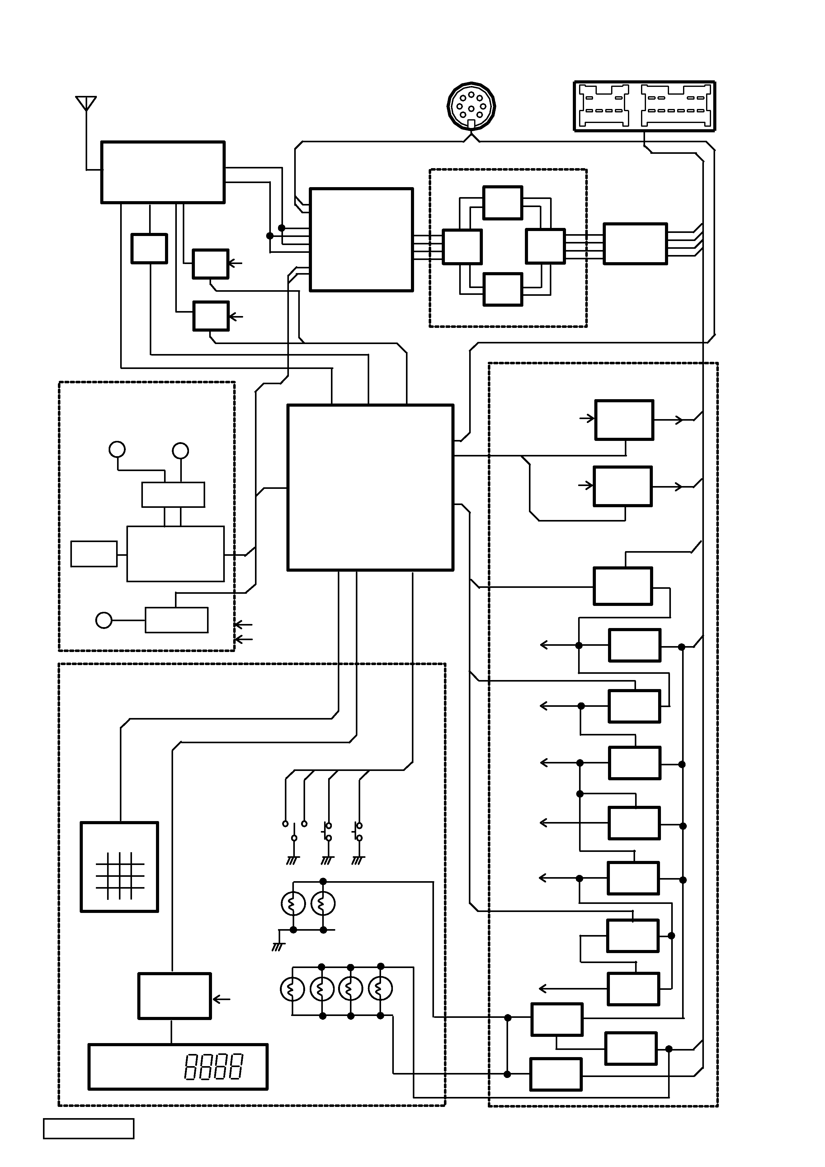
BLOCK DIAGRAM
IC301
System controller
ANT101
BL101
AM/ FM Tuner
Q103
L.P.F
IC201
Electro. volume
AUX L/ R
FM L/ R
AM- L/ R
CD L/ R
Fix. EQ block
IC601
IC602
IC603
IC604
Power amp.
30WX4ch
,i 201
AUX 8pin DIN
,i 701
NS10MW/ NS06MW
FL RL
RR FR
RR
FL
FR
RL
,p411
AMT- ON
SW
Q421
AMP- ON
SW
RADIO- ON
AMP- ON
B/ U
,p409
CD+8V
CD+8V
,p402
SYS+9V
SYS+9V
AUX ON
COMBI ON
IC901
LCD driver
LCD901
Indicator
SYS+5V
Key matrix
Escutcheon module
CD mechanism module
KS- 0
KS- 1
KS- 2
KS- 3
IC1
RF amp
IC2
Digital sig processor
with Digital servo
IC3
Servo driver
M
M
P
O
W
E
R
E
J
V
O
L
CD+8V
ANT- ON
RADIO- ON
VT
OSC
IC605
AM/ FM OSC
CD+5V
C
D
L
/
R
Power supply block
KR- 0
KR- 1
KR- 2
KR- 2
VOL- 1
VOL- 2
PWR- SW
EJ- WS
LCD- INH
LCD- CE
LCD- CLK
LCD- DATA
KS- 0
KS- 1
KS- 2
KS- 3
KR- 0
KR- 1
KR- 2
KR- 2
VOL- 1
VOL- 2 / PWR- SW / EJ- WS
LCD- INH
LCD- CE
LCD- CLK
LCD- DATA
PL+B
PL·|
ILL·{
ILL·|
IC4
Motor driver
M1
Spindle motor
M2
Sled motor
M
M3
Loading motor
AMP- ON
B/ U
AMP- ON
B/ U
,p405
SYS+12V
SYS+12V
,p407
CD ON
CD- ON
ACC
Q301
Q503
ACC- DET
ACC- ON
,p410
VDD+5V
VDD+5V
,p422
SYS+5V
SYS+5V
SYS- ON
,p401
CD+5V
CD+5V
,p417
PL+B
PL+B
,p419
,p420
R420
ILL+
ILL-
,p106
AM+B
,p107
FM+B
SYS+9V
AM- ON
FM- ON
SYS+9V
- 5 -
PN-2165M
·¡
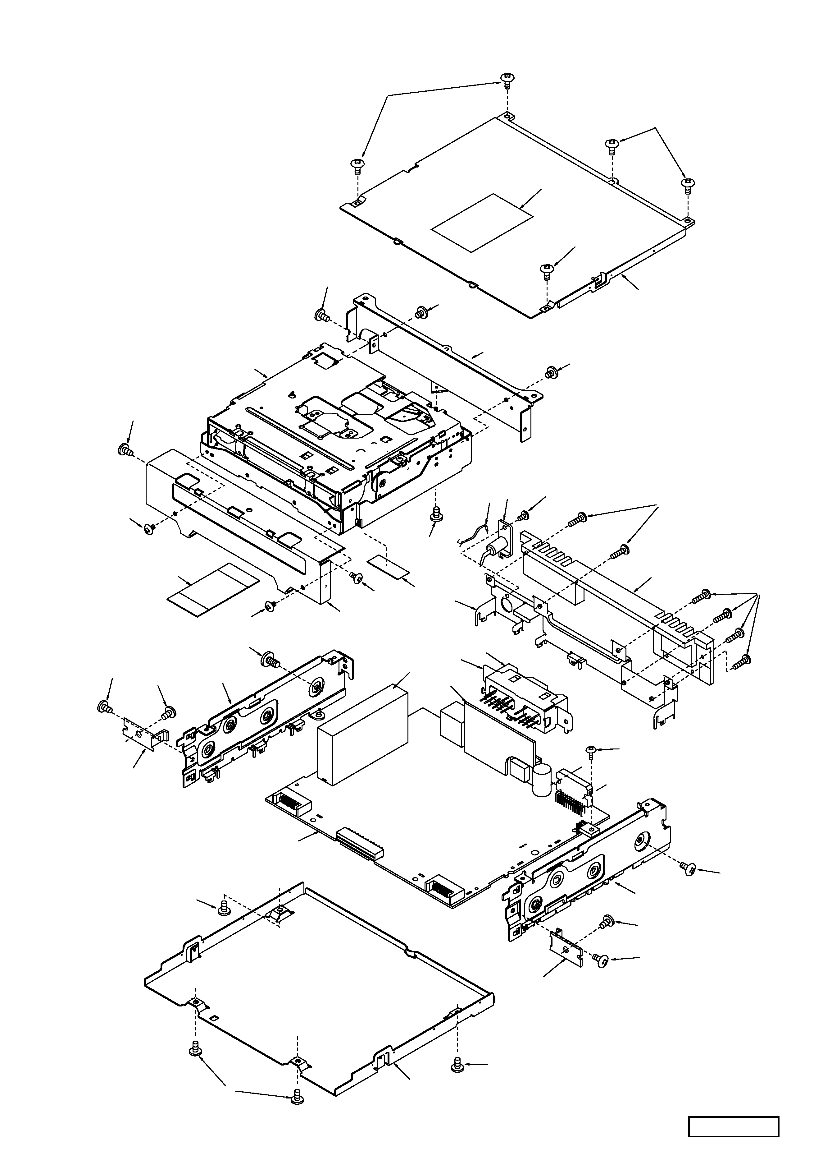
EXPLODED VIEW·EPARTS LIST
Main section
29
29
29
33
32
38
29
37
29
29
38
29
37
41
39
39
42
39
39
39
39
31 24
29
27
36
43
39
39
40
35
25
23
22
28
30
30
21
20
19
29
26
34
41
41