
3LCD DATA PROJECTOR
SERVICE MANUAL
TLP-MT1
FILE NO. 333-9906
PRINTED IN JAPAN, Dec., 1999 CS
SUPPLEMENT
--
SUMMARY
--
TLP-MT1 is based on TLP450E and TLP450U.
This service manual covers only different portions from service manual (File No. 333-9904) for
TLP450E and TLP450U.
The following parts list covers only the different parts from the base models.
For the other parts, please refer to the service manual (File No. 330-9904) of the base models.
Description
Case
Rating Label
Front Tag
Top Tag
Owner's Manual, English
Owner's Manual, French/German
Lamp Driver, 120W
Lemote Control Unit
Adaptor, 21P-RCA
PC Board, Main, PB9312
PC Board, Fan, PB9315
Part No.
23064069
23550982
23550983
23564019
23552863
23552864
23122373
23306351
23365914
23784288
23784318
Location
No.
A400
A302
A300
A301
Y201
Y202
P850
Y210
Y100
U001
U008

3LCD DATA PROJECTOR
SERVICE MANUAL
TLP450E, TLP451E
TLP650E, TLP651E
TLP450U, TLP451U
TLP650U, TLP651U
FILE NO. 330-9904
PRINTED IN JAPAN, Oct., 1999 S
TLP451, TLP651

SECTION 1
PART REPLACEMENT AND ADJUSTMENT PROCEDURES
SECTION 2
SERVICING DIAGRAMS
SECTION 3
PARTS LIST
1 . SAFETY PRECAUTION ...................................................... 3 - 1
2 . NOTICE ..................................................................................... 3 - 1
3 . ABBREVIATIONS .................................................................. 3 - 1
3-1. Integrated Circuit (IC) .................................................... 3-1
3-2. Capacitor (Cap) ................................................................ 3-1
3-3. Resistor (Res) ..................................................................... 3-1
3-11. Input PC Board ............................................................... 1-6
3-12. Lens .................................................................................... 1-6
3-13. Mirror Box ....................................................................... 1-6
3-14. LCD Block and LCD Panel ........................................... 1-7
3-15. CAM SW PC Board (Only for TLP451/651) ............ 1-9
3-16. Arm Assembly (Only for TLP451/651) ...................... 1-9
3-17. Switch (Only for TLP451/651) .................................. 1-10
3-18. Camera PC Board (Only for TLP451/651) ............. 1-10
3-19. Lamp PC Board (TLP451/651) .................................. 1-10
4 . ELECTRICAL ADJUSTMENT ....................................... 1-11
4-1. LCD Drive Adjustment .................................................. 1-12
5 . LED DISPLAY ...................................................................... 1-16
1 . PART CONFIGURATION AND THEIR SYMBOLS 2 - 1
1-1. Replacing Subminiature "CHIP" Parts ....................... 2-1
1-2. Precoutions for Part Replacement ................................ 2-2
1-3. Solid Resistor Indication .................................................. 2-2
1-4. Capacitance Indication .................................................... 2-2
1-5. Inductor Indication ........................................................... 2-3
1-6. Waveform and Voltage Measurement .......................... 2-3
2 . EACH SIGNAL FLOW ........................................................ 2 - 4
2-1. Operation at RGB Signal Input ..................................... 2-4
2-2. Video Signal ....................................................................... 2-4
2-3. Operation at Y/Pb/Pr Signal and HDTV Signal Input2-5
2-4. Camera Input Operation ................................................ 2-5
2-5. Camera Overlay Signal ................................................... 2-5
3 . BLOCK DIAGRAMS ............................................................ 2 - 7
3-1. RGB Block Diagram ........................................................ 2-7
3-2. Input Block Diagram ........................................................ 2-8
3-3. Main Block Diagram ........................................................ 2-9
3-4. Digital Block Diagram ................................................... 2-11
4 . PRINTED WIRING BOARD AND
SCHEMATIC DIAGRAM ................................................. 2-12
5 . CIRCUIT DIAGRAMS ...................................................... 2-15
5-1. Drive Circuit Diagram (for TLP650, TLP651) ........ 2-15
5-2. Drive Circuit Diagram (for TLP450, TLP451) ........ 2-19
5-3. Main Circuit Diagram (for TLP650, TLP651) ......... 2-23
5-4. Main Circuit Diagram (for TLP450, TLP451) ......... 2-27
5-5. Micon Circuit Diagram ................................................. 2-31
5-6. RGB Circuit Diagram .................................................... 2-35
5-7. Input Circuit Diagram ................................................... 2-39
5-8. Power Supply Circuit Diagram .................................... 2-42
5-9. Camera Interface Circuit Diagram ............................ 2-45
5-10. ............................................ FAN Control Circuit Diagram
2-47
6 . PC BOARDS ......................................................................... 2-49
6-1. Input PC Board ............................................................... 2-49
6-2. CAM Switch PC Board .................................................. 2-50
6-3. Main PC Board ............................................................... 2-51
6-4. RGB PC Board ................................................................ 2-55
6-5. LED PC Board ................................................................ 2-55
6-6. Sub Digital PC Board .................................................... 2-56
1 . LOCATION OF MAIN PARTS ......................................... 1 - 1
2 . LOCATION OF PC BOARDS ........................................... 1 - 1
3 . REPLACEMENT OF MECHANICAL PARTS ............ 1 - 2
3-1. Camera Arm Assembly (Only for TLP451/651) ........ 1-2
3-2. Lamp Assembly ................................................................. 1-2
3-3. Front Cover and Top Cover .......................................... 1-3
3-4. Main PC Board ................................................................. 1-3
3-5. RGB PC Board .................................................................. 1-3
3-6. Handle and Fan Assembly ............................................... 1-4
3-7. Power Supply Unit ............................................................ 1-4
3-8. Filter Assembly .................................................................. 1-5
3-9. Lamp House ....................................................................... 1-5
3-10.Optical Engine .................................................................. 1-5
CONTENTS
SAFETY PRECAUTIONS .............................................................. I
IMPORTANT PRECAUTIONS .................................................... I
IMPORTANT SAFETY INSTRUCTIONS .............................. II
4 . EXPLODED VIEWS .............................................................. 3 - 2
4-1. Packing Assembly ............................................................. 3-2
4-2. Remote Control Unit ........................................................ 3-2
4-3. Chassis Assembly ............................................................... 3-3
4-4. Arm Assembly (TLP451, TLP651) ................................ 3-4
5 . PARTS LIST ............................................................................. 3 - 5
1-1
SECTION 1
PART REPLACEMENT AND
ADJUSTMENT PROCEDURES
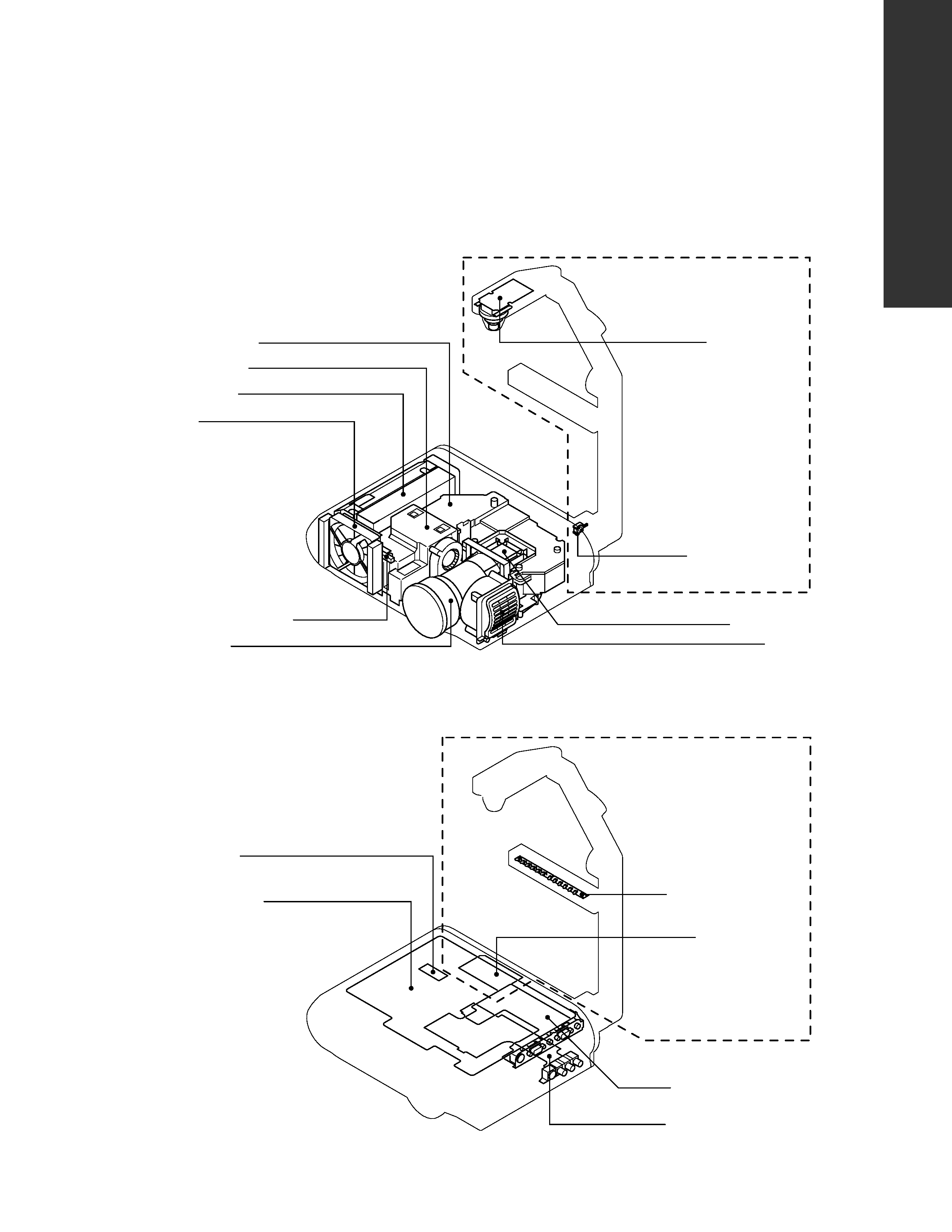
1. LOCATION OF MAIN PARTS
Fig. 1-1-1
2. LOCATION OF PC BOARDS
Fig. 1-2-1
SECTION
1
P
A
R
T
REPLA
CEMENT
AND
ADJUSTMENT
PROCEDURES
Z101 Fan
Projection Lens
P800 Power Unit
Filter
P100 Thermal Lead Switch
E200 Optical Engine
B180 Lamp House
SC01 Arm Position
Detection Switch
PC300 Camera
Unit Assembly
LCD Block
TLP451/651
U001 Main PC Board
U0031 CAM
Switch PC Board
U0032 LED PC Board
U0021RGB PC Board
U0022 Input PC Board
U007 Sub Digital
TLP451/651