
SERVICE MANUAL
PUBLISHED IN JAPAN, July, 2001
FILE NO. 2B0-200109
SX-2981
CORDLESS TELEPHONE

-- 1 --
CONTENTS
SAFETY PRECAUTIONS ...................................................................................................................... 1
OPERATING CONTROLS ................................................................................................................... 2
ALIGNMENT PROCEDURE ................................................................................................................. 3
BLOCK DIAGRAMS .............................................................................................................................. 5
SCHEMATIC DIAGRAMS ..................................................................................................................... 7
TROUBLESHOOTING HINTS ........................................................................................................... 13
IC AND TRANSISTOR VOLTAGE CHART ....................................................................................... 20
SEMICONDUCTOR LEAD IDENTIFICATION ................................................................................... 25
ELECTRICAL PARTS LOCATION ..................................................................................................... 29
WIRING DIAGRAMS .......................................................................................................................... 32
EXPLODED VIEW AND MECHANICAL PARTS LIST ...................................................................... 34
PARTS LIST ........................................................................................................................................ 36
ASSEMBLY PARTS LIST ................................................................................................................... 49
SPECIFICATIONS .............................................................................................................................. 50
SAFETY PRECAUTIONS
Before returning any models to the customer, a safety check of the entire instrument should be made.
The service technician must be sure that no protective device built into the instrument by the manufacturer
has become defective or inadvertently degraded during servicing.
1. WARNING:
Alterations of the design or circuitry of these models should not be made.
Any design changes or additions such as, but not limited to, circuit modifications, auxiliary speaker
jacks, switches, grounding, active or passive circuitry, etc. may alter the safety characteristics of these
models and potentially create a hazardous situation for the user.
Any design alterations or additions will void the manufacturer's warranty and will further relieve the
manufacturer of responsibility for personal injury or property damage resulting therefrom.
2. PRODUCT SAFETY NOTICE
Many electrical and mechanical parts in this chassis have special characteristics. These characteristics
often pass unnoticed and the protection afforded by them cannot necessarily be obtained by using
replacement components rated for higher voltage, wattage, etc. Replacement parts that have these
special safety characteristics are identified in this manual and its supplements; electrical components
having such features are identified by a
in the schematic diagram and the parts list. Before replacing
any of these components, read the parts list in this manual carefully. The use of substitute replacement
parts that do not have the same safety characteristics as specified in the parts list may create shock,
fire or other hazards.
-- 2 --
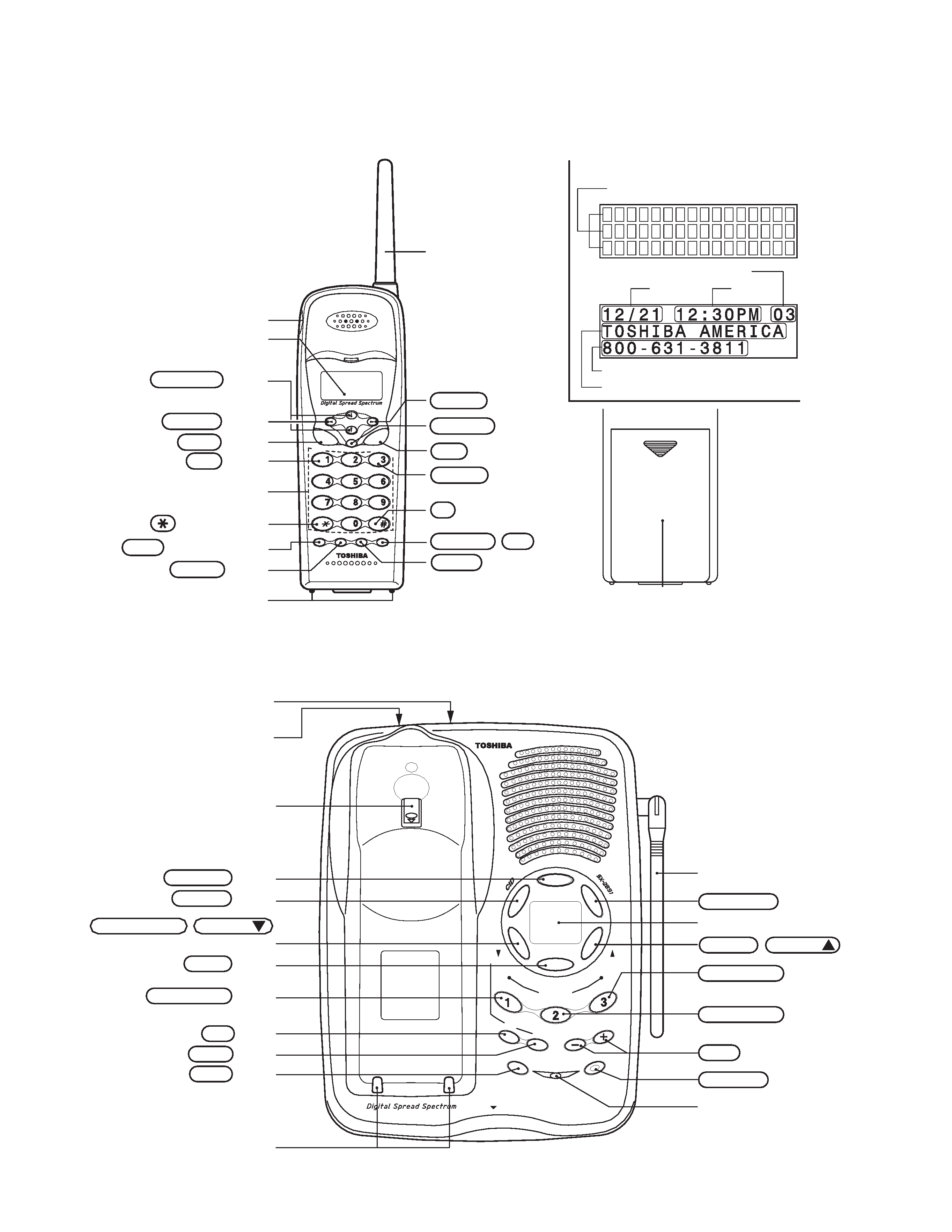
OPERATING CONTROLS
BASE UNIT CONTROLS
REDIAL
L.D.
LOCAL
MEM
TONE
PAUSE
FUNCTION DELETE
CHANNEL
FLASH
VOL/RING
SELECT
TALK
CID
ABC
JKL
TUV
OPER
DEF
MNO
WX
YZ
PQ
RS
GHI
Dialpad
Charging contact
LCD Display
Handset Jack
Antenna
VOL/RING Button
TALK Button
L.D. Button
(TONE) Button
PA
MEM (Memory) Button
USE Button
FUNC Button
DELETE
CH Button
CID Button
FLASH Button
LOCAL Button
SELECT Button
(PULSE) Button
#
REDIAL Button
DELETE
REC/MEMO
ANSWER
STOP
SKIP
REPEA
T
FF
REW
MIC
CO
RDL
ESS TELEPHO
NE
D
IG
ITA
L C
ALL
ER ID
/ANSWERING
SYS
TE
M
MAIL BOX
SELECT
SELECT
SET
MENU
VOL
PAGE
SPEAKER
IN USE
CHARGE
Hook
DC IN 9V Jack
TEL LINE Modular Jack
Antenna
LED Display
PAGE Button
REC/MEMO Button
SKIP FF / SELECT
Button
STOP Button
SPEAKER Button
IN USE / CHARGE LED
DELETE Button
Charging Contact
MAIL BOX 1 Button
MAIL BOX 3 Button
MAIL BOX 2 Button
ANSWER Button
VOL Button
MENU Button
SET Button
REPEAT REW / SELECT
Button
HANDSET CONTROLS
Rechargeable
Battery Pack (back)
LCD
Number of calls
Dot matrix display
Date
Time
Caller's telephone number
Caller's name
-- 3 --
ALIGNMENT AND ADJUSTMENT
BASE UNIT
Transmitter Section
Connections
· Spectrum Analyzer
Alignment Point Location on Base Main PCB and Base RF PCB
AC Adapter
(120V 60Hz)
Base Unit
Test Point
(J301)
Spectrum Analyzer
RF PCB
CT1
J1
J2
Base Main PCB
Remove solder
before alignment
J301
Base RF PCB
Test Point
Alignment Procedure
Step
Adjustment
Remarks
1
CT1
(Frequency Adjust)
Connect the Spectrum Analyzer to test point (J301).
Adjust CT1 so that the frequency is 916.992 MHz.
2
--
Confirm that the power instructions of the Spectrum analyzer reaches
11.5 3.0 dBm. After alingnment, be sure to re-solder the pattern.
Preset
a) Turn on AC power while the "PAGE" key is being depressed.
b) Before alignment, be sure to remove solder on the pattern of RF PCB (refer to the illus. below).
-- 4 --
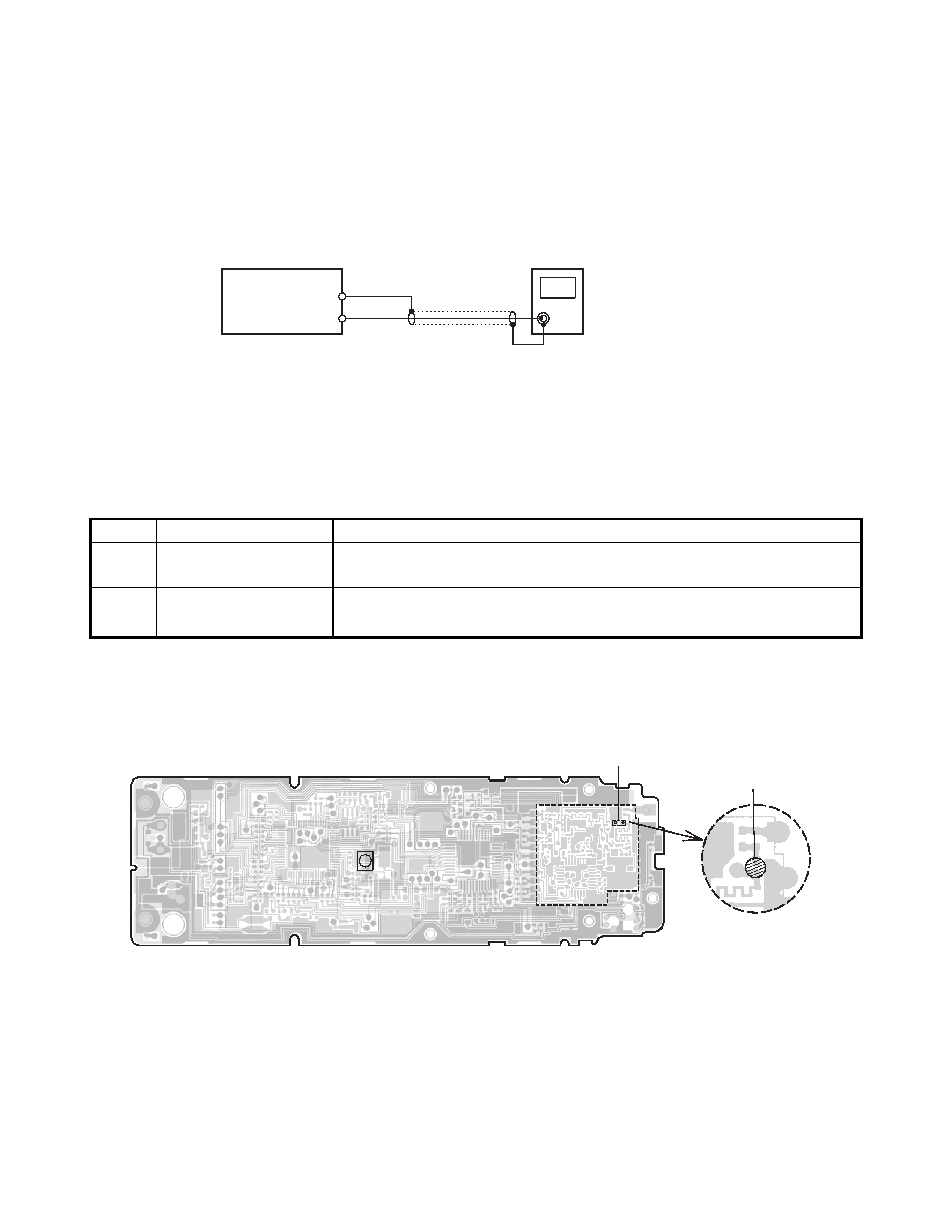
Alignment Point Location on Handset Main PCB and Handset RF PCB
Handset Unit
Test
Point
(J801)
Spectrum Analyzer
CT601
Handset PCB
Handset RF PCB
Remove solder
before alignment
J801
Test Point
Alignment Procedure
Step
Adjustment
Remarks
1
CT601
(Frequency Adjust)
Connect the Spectrum Analyzer to test point (J801).
Adjust CT601 so that the frequency is 916.992 MHz.
2
--
Confirm that the power instructions of the Spectrum analyzer reaches
11.5
3.0 dBm.After alignment, be sure to re-solder the pattern.
HANDSET UNIT
Transmitter Section
Connections
· Spectrum Analyzer
Preset
a) Turn the power ON (Connect battery) while depressing " " and "#" keys.
b) Press "1" key.
c) Before alignment, be sure to remove solder on the pattern of RF PCB (refer to the illus. below).