DVD VIDEO/AUDIO PLAYER
SERVICE MANUAL
Aug., 2002 5
FILE NO. 813-200201
SD-4800
SUMMARY
This service manual covers only the different points from the service manual, file no. 810-200210,
for model SD-3800 since SD-4800 is basically the same designing as SD-3800.
Please refer to the file no. 810-200210 for other information.
SUPPLEMENT
DIGITAL VIDEO
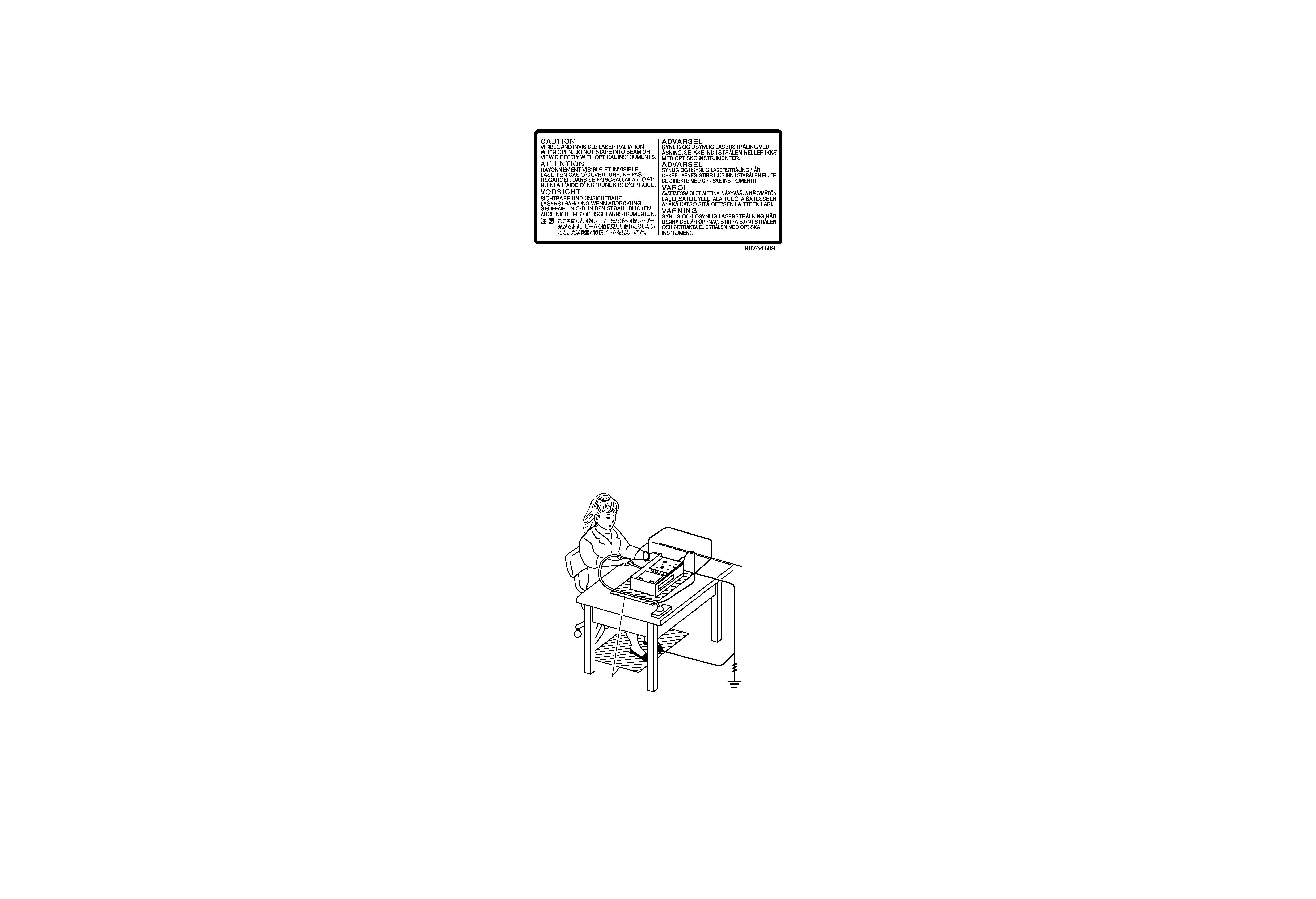
LASER BEAM CAUTION LABEL
When the power supply is being turned on, you may not remove this laser cautions label. If it removes, radiation of a laser
may be received.
PREPARATION OF SERVICING
Pickup Head consists of a laser diode that is very susceptible to external static electricity.
Although it operates properly after replacement, if it was subject to electrostatic discharge during replacement,
its life might be shortened. When replacing, use a conductive mat, soldering iron with ground wire, etc. to
protect the laser diode from damage by static electricity.
And also, the LSI and IC are same as above.
1M9
Ground conductive
wrist strap for body.
Soldering iron
with ground wire
or ceramic type
Conductive mat
The ground resistance
between the ground line
and the ground is less than 109.

1. PRINTED WIRING BOARD AND SCHEMATIC DIAGRAM
2. BLOCK DIAGRAMS
2-1. Overall Block Diagram
2-2. Output Block Diagram
CONTENTS
SECTION 3
SERVICING DIAGRAMS
SECTION 4
PARTS LIST
SAFETY PRECAUTION
NOTICE
ABBREVIATIONS
1. Integrated Circuit (IC)
2. Capacitor (Cap)
3. Resistor (Res)
4. EXPLODED VIEWS
4-1. Chassis Assembly (Type A)
4-2. Chassis Assembly (Type B)
5. PARTS LIST
3. Circuit Diagram
3-1. Output Circuit Diagram
4. PC Board
4-1. Output PC Board
1
2
3
4
5
1
2
3
4
5
VCC+9V
GND
VEE-9V
GND
VDD+5V
VCC+9V
GND
VEE-9V
GND
VDD+5V
RGBON
SOUTX
ASP1
ASP2
IPXO
IPXI
GND
CV
-INPUT
VGND
Y
-INPUT
VGND
C-INPUT
VGND
Y(I/P)-INPUT
VGND
Cb(I/P)-INPUT
VGND
Cr(I/P)-INPUT
VGND
RGBON
SOUTX
ASP1
ASP2
IPXO
IPXI
GND
CV
-OUTPUT
VGND
Y
-OUTPUT
VGND
C-OUTPUT
VGND
Y(I/P)-OUTPUT
VGND
Cb(I/P)-OUTPUT
VGND
Cr(I/P)-OUTPUT
VGND
1
2
3
4
5
6
7
8
9
10
11
12
13
14
15
16
17
18
19
1
2
3
4
5
6
7
8
9
10
11
12
13
14
15
16
17
18
19
GND
LDMP
TOPN
LDMN
TCLS
NC
NC
LEFT
COMMON(GND)
DOWN
ENTER
RIGHT
UP
GND
5V
TXD
CTS
RXD
RTS
FMN
FMP
GND
LMT
DMN
DMP
VCC
DMFG
PWON
E+5V
VDD+5V
VDD+3.3V
VDD+2.5V
GND
GND
M+8V
MGND
VKK-34V
F-
F+
PWON
E+5V
VDD+5V
VDD+3.3V
VDD+2.5V
GND
GND
M+8V
MGND
VKK-34V
F-
F+
GND
EVER+5V
POWER LED
POWER KEY
1
2
3
4
5
6
7
8
9
10
11
12
1
2
3
4
5
6
7
8
9
10
11
12
1
2
3
4
5
6
7
8
1
2
3
4
5
6
7
8
1
2
3
4
5
6
1
2
3
4
5
6
1
2
3
4
1
2
3
4
1
2
3
4
5
6
7
1
2
3
4
5
6
5P
Press-fit
12P
Press-fit
FFC 1.25mm 6P W502
FFC 1mm 8P W503
FFC 2mm 4P
W102
FFC 1mm 19P
W302
CNY02
Board-in
CN802
PUH
TRAY
MOTOR
CN502
CN503
CN701
CN101
CN603
CN103
CN102
CN801
Board-in
CNX01
CN302
CN104
CN601
EU05 OUTPUT
EU02
POWER
EU04 POWER-SW
EU03 FRONT
EU01 MAIN
Mechanism
RST
OX
PWRCNT
E+5V
HMUTE
DSPRST
DSPSIO_D-M
DSPSIO_M-D
DSPCKX
DSTBX
GND
VKK-34V
F+
F-
RST
OX
PWRCNT
E+5V
HMUTE
DSPRST
DSPSIO_D-M
DSPSIO_M-D
DSPCKX
DSTBX
GND
VKK-34V
F+
F-
1
2
3
4
5
6
7
8
9
10
11
12
13
1
2
3
4
5
6
7
8
9
10
11
12
13
FFC 1mm 13P
W603
1
2
3
4
5
6
7
8
9
10
11
12
13
14
15
16
17
18
19
20
21
22
23
1
2
3
4
5
6
7
8
9
10
11
12
13
14
15
16
17
18
19
20
21
22
23
VCC
RF
LD2
MON2
VOR2
GND
VREF
VCC
F0
E0
A0
D0
C0
B0
F+
T-
T+
F-
VCC
GND
LD
MON
VOR
W501
FFC 1mm 23P
CN501
IED958IN
GND
HMUTE
POWER
ON
FL
OUTPUT
GND
FR
OUTPUT
SL
OUTPUT
GND
SR
OUTPUT
C
OUTPUT
GND
SW
OUTPUT
HMUTES
HMUTE
CSW
IED958OUT
GND
HMUTE
POWER
ON
FL
OUTPUT
GND
FR
OUTPUT
SL
OUTPUT
GND
SR
OUTPUT
C
OUTPUT
GND
SW
OUTPUT
HMUTES
HMUTE
CSW
1
2
3
4
5
6
7
8
9
10
11
12
13
14
15
1
2
3
4
5
6
7
8
9
10
11
12
13
14
15
FFC 1mm 15P
W901
CNY01
CN901
1. PRINTED WIRING BOARD AND SCHEMATIC DIAGRAM
Fig. 3-1-1
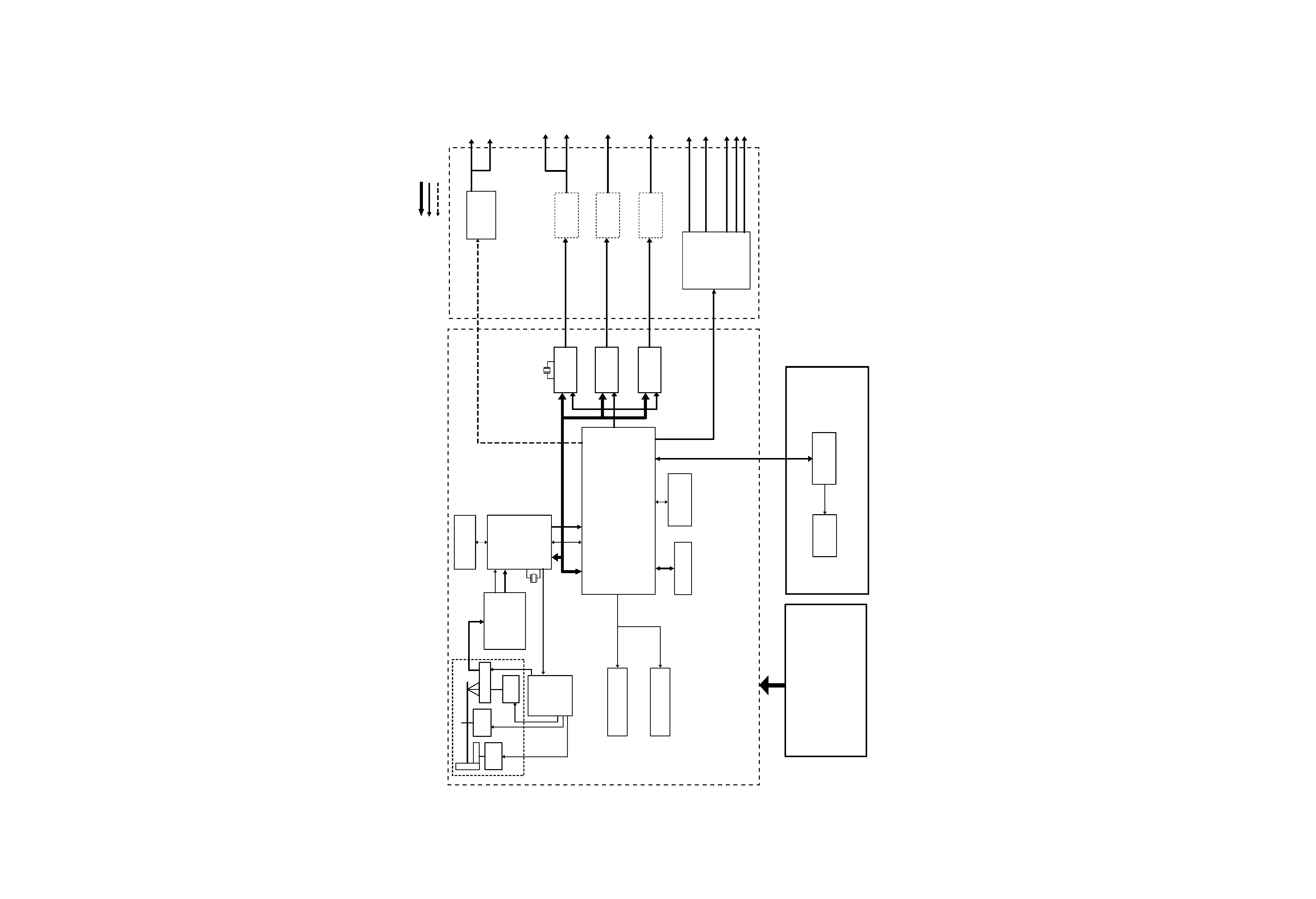
PUH
Display-CPU
Display
(FL)
Feed
Motor
Tray
Motor
PUH Driver
Motor Driver
1M-DRAM
Decryption,
Video Process,MPEG-2 Decoder
Dolby-Digital Decoder, OSD
MAIN CPU
64M-S-DRAM
1chip-SERVO
Data Processor
SPM
VIDEO LPF
with
AMPLIFIRE
Composite
Video Out
S Video Out
Y,CB,CR
Video
Out
Coaxial
Digital
TOS Link Digital
Audio Out
22.5792
MHz
E2PROM
RF Amp.
Data/Control Bus
DVD AV Data
SP DIF Data
Buffer
LPF &
Amplifier
Audio Out
FL, FR Analog
Audio Out
SL, SR Analog
Audio Out
Center SW
Analog
Audio Out
2ch Analog
Audio Out
SW POWER SUPPLY
FRONT DISPLAY UNIT
MAIN PROCESSOR UNIT
AUDIO/VIDEO OUTPUT UNIT
IC502
TA1323F
X501
Xtal
27MHz
IC503
BA5813FM
IC307
S24C02BFJ
E2PROM
IC308
S24C02BFJ
IC402
M11B11664A-30T
IC401
TC94A03F
IC101
TMP87CH75F-3D68
IC305
MT48LC2M32B2
32M-FRAM
IC309
MBM29DV324BE
IC902
AD1958
IC903
PCM1742KE
IC904
PCM1742KE
IC306
ZR36750
ICY02
TC74HCU04A
ICY01
NJM4580E
LPF &
Amplifier
Audio Out
ICY06
NJM4580E
LPF &
Amplifier
Audio Out
ICY05
NJM4580E
ICX01
MM1568
PLL+DAC
Audio-DAC
Audio-DAC
Fig.3-2-1
2. BLOCK DIAGRAMS
2-1. Overall Block Diagram