
!"#$%&''()&%&*+",&
PUBLISHED IN JAPAN, Nov., 1998
'&#-.!&(/0,10%
2.%&(,"3((456789:;
FT-7007LR
FT-7007LBR

1
CONTENTS
SAFETY PRECAUTIONS ............................................................................................................ 1
OPERATING CONTROLS ........................................................................................................... 2
ALIGNMENT PROCEDURE ........................................................................................................ 3
BLOCK DIAGRAMS ..................................................................................................................... 7
SCHEMATIC DIAGRAMS ............................................................................................................ 9
TROUBLESHOOTING HINTS ................................................................................................... 13
IC AND TRANSISTOR VOLTAGE CHART ............................................................................... 20
SEMICONDUCTOR LEAD IDENTIFICATION ........................................................................... 24
ELECTRICAL PARTS LOCATION ............................................................................................. 26
WIRING DIAGRAM .................................................................................................................... 27
EXPLODED VIEW AND MECHANICAL PARTS LIST ............................................................... 28
PARTS LIST ............................................................................................................................... 32
ASSEMBLY PARTS LIST .......................................................................................................... 40
SPECIFICATIONS ..................................................................................................................... 41
SAFETY PRECAUTIONS
Before returning any models to the customer, a safety check of the entire instrument should be made. The service
technician must be sure that no protective device built into the instrument by the manufacture has become defective
or inadvertently degraded during servicing.
1.WARNING:
Alterations of the design or circuitry of these models should not be made.
Any design changes or additions such as, but not limited to, circuit modifications, auxiliary speaker jacks, switches,
grounding, active or passive circuitry, etc. may alter the safety characteristics of these models and potentially
create a hazardous situation for the user.
Any design alterations or additions will void the manufacturer's warranty and will further relieve the manufacturer of
responsibility for personal injury or property damage resulting therefrom.
2.PRODUCT SAFETY NOTICE
Many electrical and mechanical parts in this chassis have special characteristics. These characteristics often pass
unnoticed and the protection afforded by them cannot necessarily be obtained by using replacement components
rated for higher voltage, wattage, etc. Replacement parts that have these special safety characteristics are identified
in this manual and its supplements; electrical components having such features are indentified by a
in the
schematic diagram and the parts list. Before replacing any of these components, read the parts list in this manual
carefully. The use of substitute replacement parts that do not have the same safety characteristics as specified in
the parts list may create shock, fire or other hazards.
2
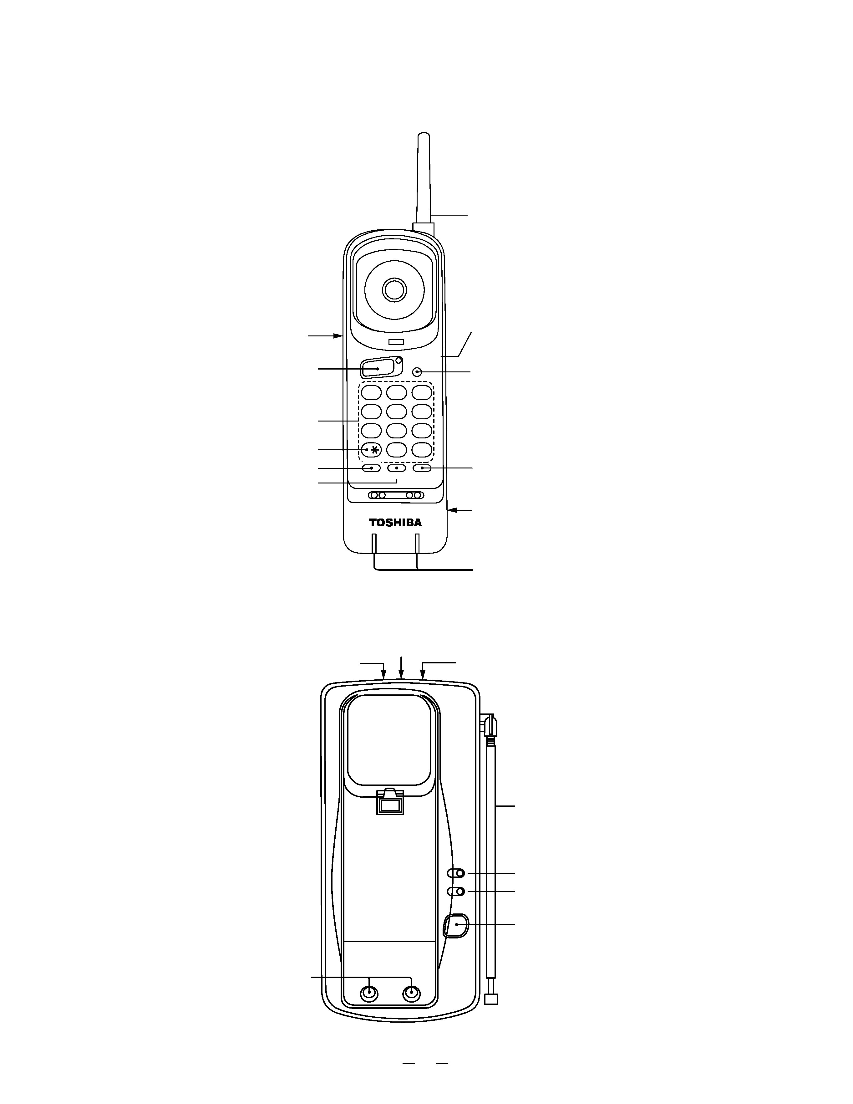
OPERATING CONTROLS
HANDSET CONTROLS AND FUNCTIONS
BASE UNIT CONTROLS AND FUNCTIONS
TALK/BATT
CHANNEL
2
ABC
3
DEF
1
5
JKL
6
MNO
4
GHI
8
TUV
9
WX
YZ
7
0
OPER
#
MEM
FLASH RDL/P
25CHANNEL
COMPANDOR
NOISE
REDUCTION
SYSTEM
FT-7007
TOSHIBA
PAGE
POWER
CHARGE
TONE
PQ
RS
25CHANNEL
Helical Antenna
Speed Dial Index Card(back)
Write all your memorized telephone
numbers.
TALK/BATT.LOW LED
TALK Button
CHANNEL Button
0-9, æ
, # Buttons
TONE
MEM Button
REDIAL/PAUSE Button
FLASH Button
Rechargeable Battery Pack
(back)
Charging Contacts
Telephone Modular Jack
DC in 9V Jack
T-P(TONE-PULSE) Switch
Base Antenna
CHARGE LED
PAGE Button
Charging Contacts
POWER LED
3
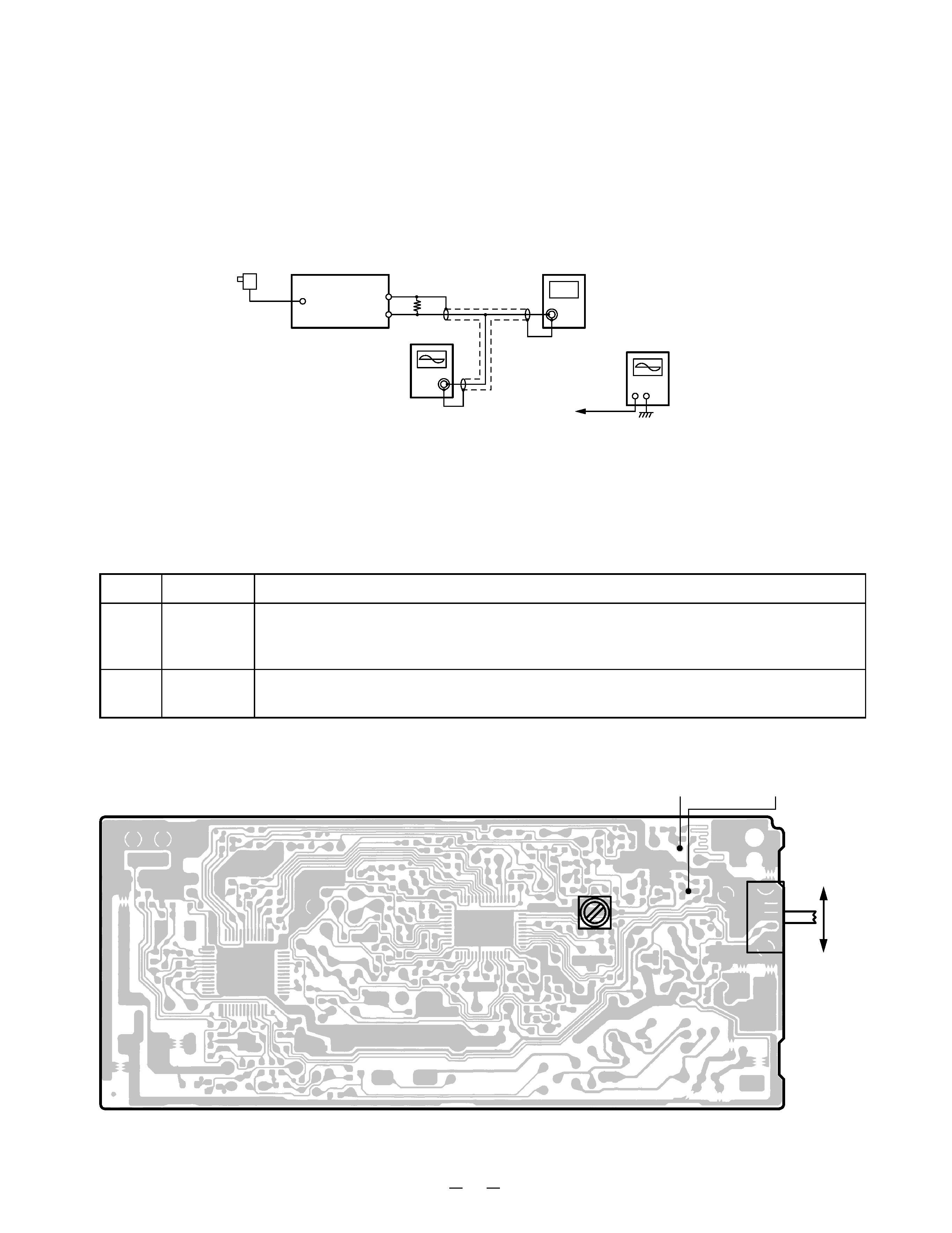
ALIGNMENT PROCEDURE
Base Unit / Transmitter
Test Equipment Required and Connections
· Oscilloscope
· Dummy Load, 50-ohm
· Frequency Counter
· AC Power Supply : 120V, 60Hz (With AC Adapter)
Preset
a) Set T/P SW to Pulse Mode.
b) Turn on AC power while the Page key is being depressed.
c) Release the Page key 2 seconds later, then the TX Mode is entered (CH21).
Alignment Procedure
Alignment Point Location on Main PCB
Step
Adjustment
Remarks
1L8
Connect the oscilloscope across a 50-ohm load to RF test point.
Set the digital voltmeter at the test point of TX VCO.
Adjust L8 to indicate DC 2.8V ±0.05V.
2
!
Connect the frequency counter across a 50-ohm dummy load to RF test point. Make
sure that the frequency is 46.770 MHz ±1500Hz.
AC Adapter
(120V 60Hz)
BASE Unit
Dummy Load
(50-ohm)
RF Test
Point
Frequency Counter
Digital Voltmeter
TX VCO
Test Point
Oscilloscope
T/P SW
L8
S1
P
T
RF Test Point
TX VCO Test Point
4
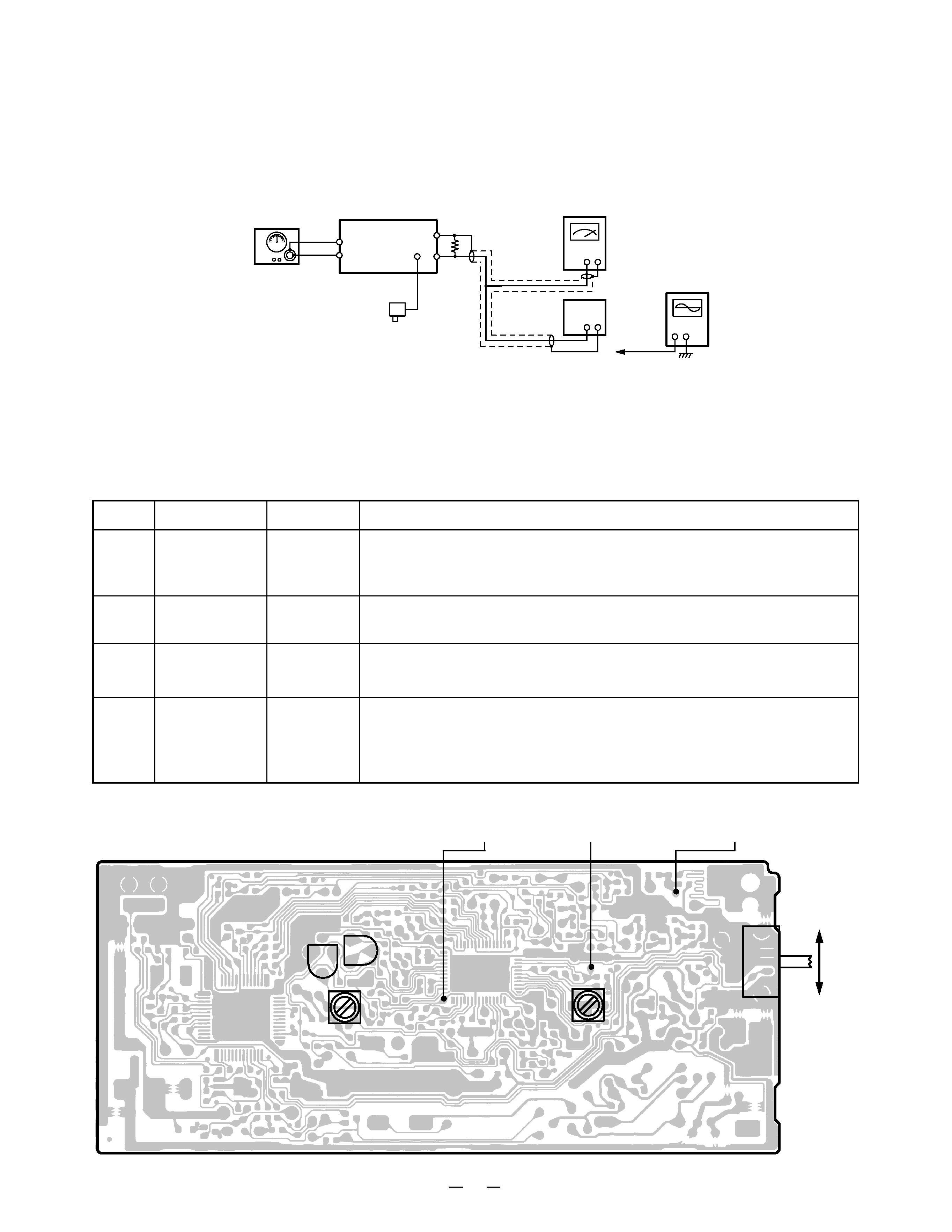
Receiver
Test Equipment Required and Connections
· SG: RF Signal Generator, 49.830MHz
· Dummy Load, 600-ohm
· Digital Voltmeter
· AF SSVM
· SINAD Meter
AC Adapter
(120V 60Hz)
Digital Voltmeter
BASE Unit
RF Test
Point
TEL Jack
SG
MOD=1kHz
DEV=±3kHz
AF SSVM
SINAD
Meter
Dummy Load
(600-ohm)
Alignment Point Location on Main PCB
Preset
a) Set T/P SW to Pulse Mode.
b) Turn on AC power while the Page key is being depressed.
c) Release the Page key 2 second later, then the TX Mode is entered (CH21).
d) Press the Page key 4 times, then the DUPLEX Mode is entered (CH21).
Alignment Procedure
T/P SW
L4
S1
P
T
DISCRI Test Point
RX VCO Test Point
L2
RT2
RT1
RF Test Point
Step
Preset to
Adjustment
Remarks
1
SG: 1mV
No modulation
L4
Connect the SG to the RF test point.
Connect the digital voltmeter to the test point of the RX VCO.
Adjust L4 to indicate DC 3.3V ±0.05V.
2
SG: 1mV
No modulation
L2
Set the digital voltmeter at the test point of DISCRI.
Adjust L2 to indicate 2.0V ±0.05V.
3
SG: 1mV
1kHz ±3kHz
deviation
RT2
Connect the AF SSVM to the TEL LINE through a 600-ohm dummy
load, then adjust RT2 to indicate AC -6dBm ±0.5dBm.
4
SG: 0.2"V
No modulation
RT1
Press the Page key 2 times.
Turn RT1 to fully clockwise and confirm
the STATUS LED turns off.
Then adjust RT1 to turn to counterclockwise slowly where the STATUS
LED just turns on.