U
UX
X--11
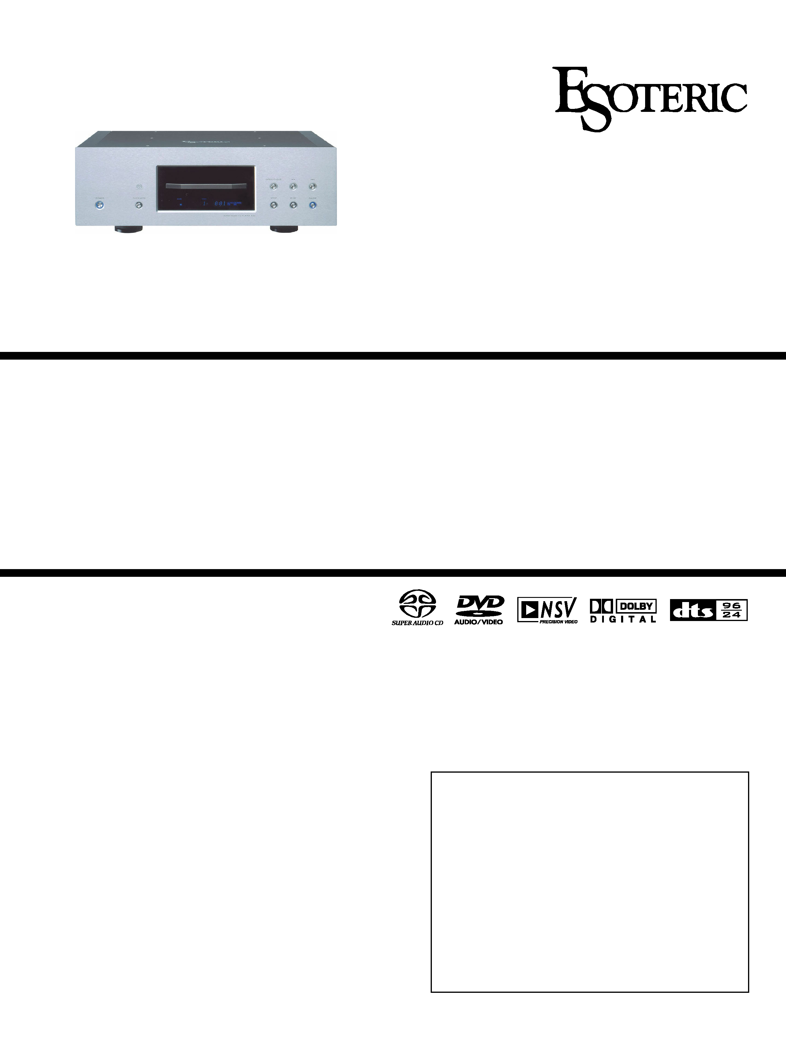
SERVICE MANUAL
DVD/DVD-A/CD/SACD PLAYER
Effective : August, 2004 8C0362
S-0127A
NOTES
PC boards shown are viewed from parts side.
The parts with no reference number or no parts number in the
exploded views are not supplied.
As regards the resistors and capacitors, refer to the circuit diagrams
contained in this manual.
£
Parts marked with this sign are safety critical components. They
must be replaced with identical components - refer to the appropriate
parts list and ensure exact replacement.
Parts of [ ] mark can be used only with the version designated.
CONTENTS
1 SPECIFICATIONS
2
2 BLOCK DIAGRAM
3
3 ADJUSTMENTS
4
4 EXPLODED VIEWS AND PARTS LIST
5
5 PC BOARDS AND PARTS LIST
11
6 INCLUDED ACCESSORIES
26
General
System ..................................DVD-Video, DVD-Audio, DVD-R/RW,
Video-CD, SACD, and CD
Power supply ..............................AC 230 V, 50 Hz (Europe model)
........................................AC 120 V, 60 Hz (U.S.A./Canada model)
......................................................AC 220 V, 60 Hz (Korea model)
Power consumption ..............................................................45 W
Weight................................................................25 kg (55-1/16 lb)
External dimensions (W x H x D) ..................442 x 153 x 353 mm
(17-3/8" x 6" x 13-7/8")
Operating temperature................................................+5°C ~ +35°C
Operating humidity..........................5% to 85% (no condensation)
Storage temperature ................................................20°C ~ +55°C
Video Output
S-Video output (S1/S2)
Y (luminance) - Output level ................................1 Vp-p (75 )
C (color) - Output level ................................286 mVp-p (75 )
Jacks ....................................................................S-VIDEO jack
Video output
Output level ........................................................1 Vp-p (75 )
Jacks ..........................................................................RCA jack
Component video output (Y, PB, PR)
Y-Output level ..................................................1.0 Vp-p (75 )
PB, PR-Output level ..........................................0.7 Vp-p (75 )
Jacks ........................................................................ BNC jacks
D1/D2 video output (Y, PB, PR)
Y-Output level ..................................................1.0 Vp-p (75 )
PB, PR-Output level ..........................................0.7 Vp-p (75 )
Jacks ........................................................................D terminal
DVI-D video output (HDCP compatible digital RGB)
Jacks ..............DVID 24pin (conform to TMDS, single link only)
Audio output (Analog Audio)
Jacks ......................................................XLR jacks (2 channel) x 1
RCA jacks (5.1 channel) x 1
Maximum Output level (1 kHz, full scale) ..............2.5 Vrms (RCA)
2.3 Vrms (XLR)
Nominal Output level (1 kHz, full scale 20dB) ..250 mVrms (RCA)
230 mVrms (XLR)
Frequency response ..............................5Hz - 80 kHz (DVD-Audio)
Signal-to-Noise Ratio (S/N)..........................112 dB (SACD, 1 kHz)
Dynamic range ............................................106 dB (SACD, 1 kHz)
Total harmonic distortion............................0.001% (SACD, 1 kHz)
Decodable format ............................DTS, DTS 96/24, Dolby Digital
PCM 44.1 kHz-192 kHz/16-24 bit, DSD
Audio output (Digital Audio)
OPTICAL ..........................Optical digital jack x 1, 15 to 21 dBm
COAXIAL ............................................RCA jack x 1, 0.5 Vp-p/75
Word Synchronization input format
Jack ........................................................................................BNC
Input level ................................................................4.5 Vp-p/75
The main unit can accept and synchronize to the following
frequencies received from external devices:
44.1kHz, 48kHz, 88.2kHz, 96kHz, 100kHz, 176.4kHz, 192kHz
as well as frequencies which are 96% of these values, in the
4% DOWN mode.
Accessories
Power cord x 1
Remote Control Unit (RC-942) x 1
Batteries (AA, R6, SUM-3) x 2
Screwdriver x 1
Felt x 3
Warranty card x 1
Owner's manual x 1
· Design and specifications are subject to change without notice.
· Weight and dimensions are approximate.
1 SPECIFICATIONS
2
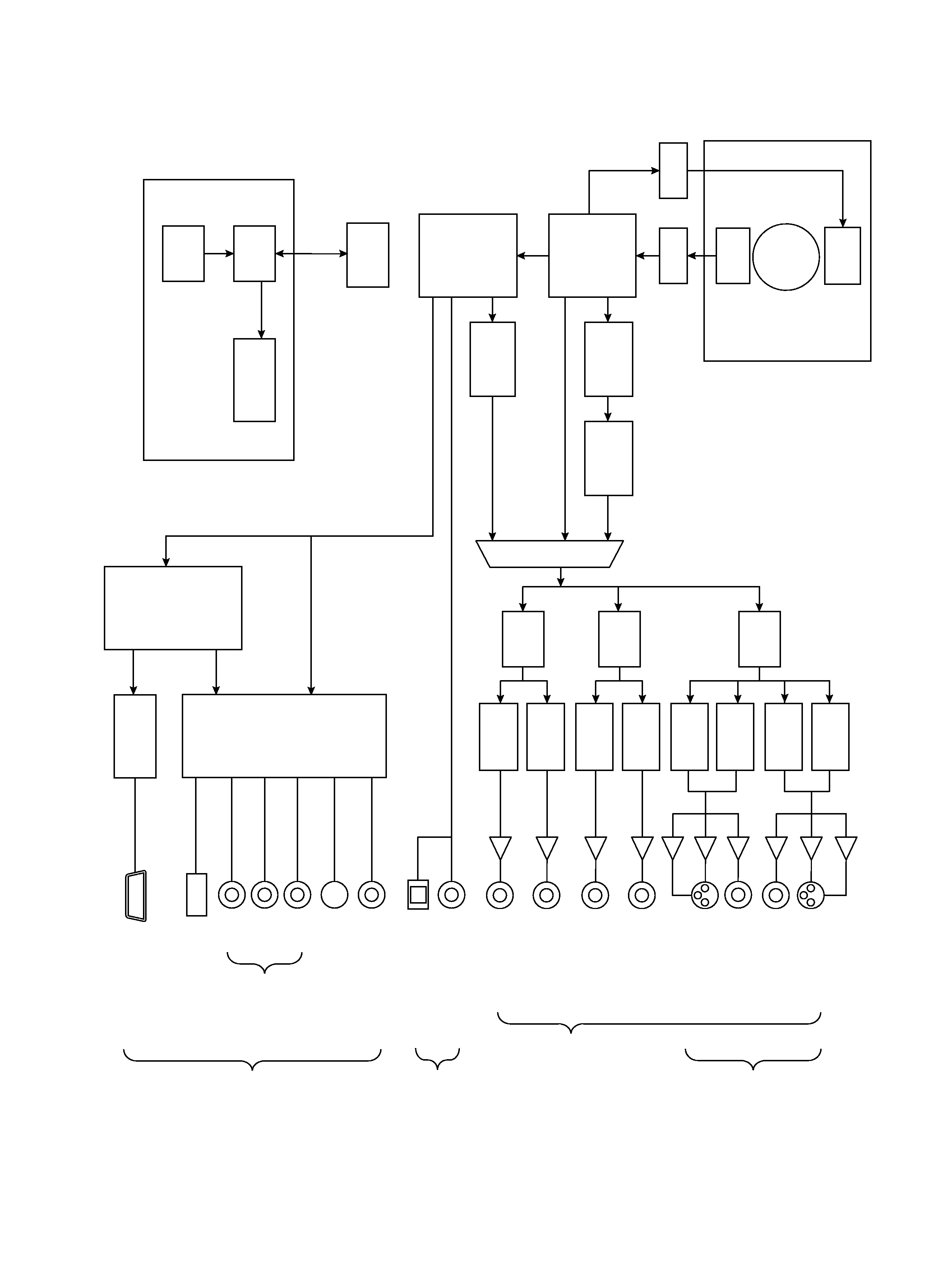
2 BLOCK DIAGRAM
3
SACD
CD
SACD
VRDS
UNIT
FRONT
P
ANEL
CD
DVD
Spindle
Motor
Front
End
DSP
SACD
Decoder
PCM
Converter
Digital
Filter
D/A
Converter
+
+
Balanced
Front
L
ch
Balanced
Front
R
ch
Front
L
ch
AUDIO
OUT
(2ch)
AUDIO
OUT
(5.1ch)
VIDEO
OUT
Component
V
ideo
DIGIT
AL
OUT
Front
R
ch
Surround
L
ch
Surround
R
ch
Center
Subwoofer
Coaxial
Optical
Composite
V
ideo
S-V
ideo
Y
C
B/P
B
C
R/P
R
D1/D2
DVI-D
(HDCP)
D/A
Converter
D/A
Converter
D/A
Converter
D/A
Converter
D/A
Converter
D/A
Converter
D/A
Converter
DVI
T
ransmitter
Digital
Filter
Digital
Filter
MPEG-2
Decorder
V
ideo
Encoder
I/P
Converter
Driver
Optical
Pickup
RF
Amp
Back
End
MPU
I/F
MPU
FL
Display
Key
SW
Audio
DSP
3 ADJUSTMENTS
4
R232
R235
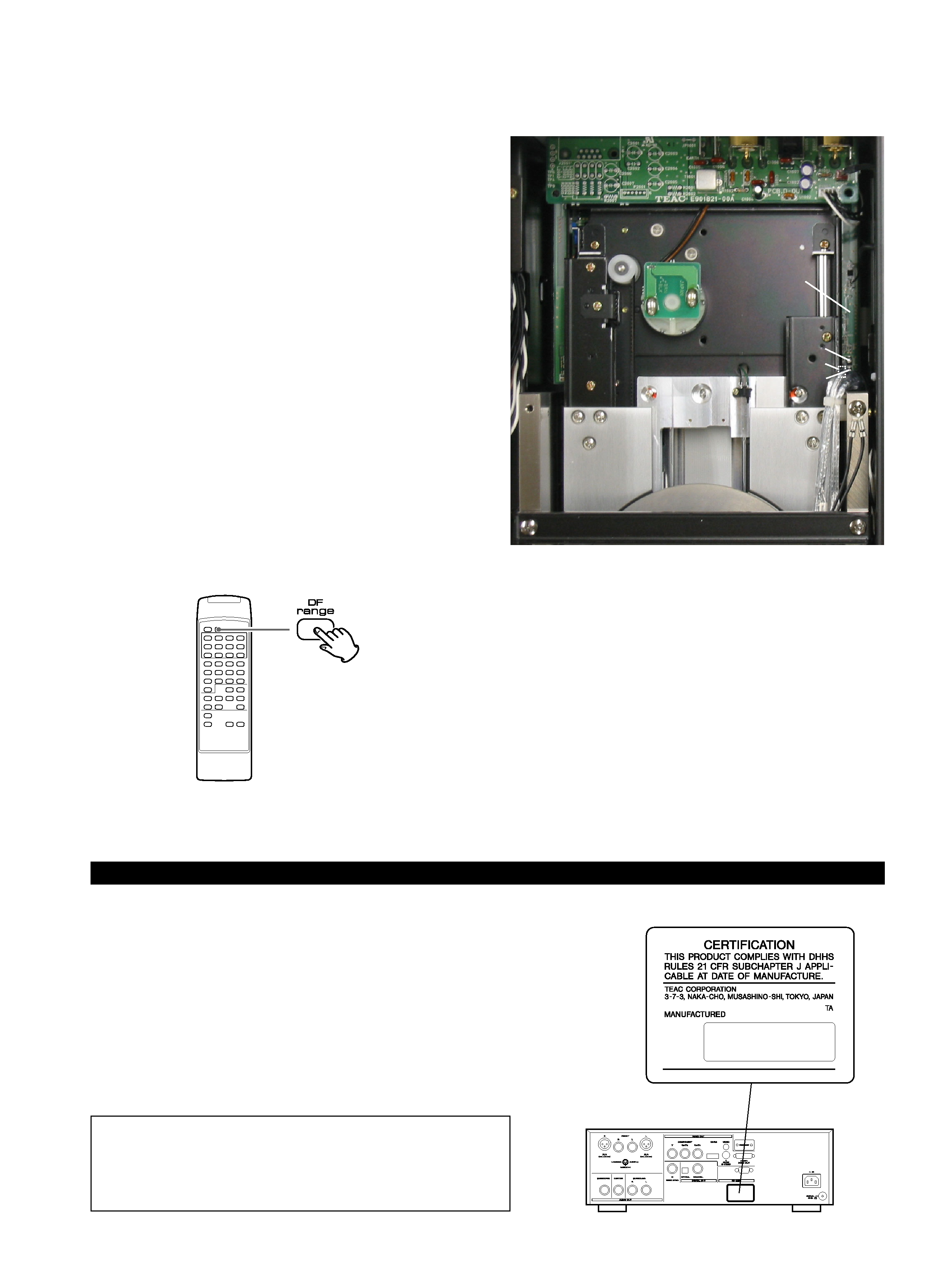
CORE PCB
P205 (Bottom Side)
SAFETY INFORMATION
This product has been designed and manufactured according to FDA
regulations "title 21, CFR, chapter 1, subchapter J, based on the Radiation
Control for Health and Safety Act of 1968", and is classified as a class 1
laser product. There is no hazardous invisible laser radiation during
operation because invisible laser radiation emitted inside of this product
is completely confined in the protective housings.
The label required in this regulation is shown 1.
OCAUTION
USE OF CONTROLS OR ADJUSTMENT OR PERFORMANCE OF
PROCEDURES OTHER THAN THOSE SPECIFIED HEREIN MAY RESULT IN
HAZARDOUS RADIATION EXPOSURE.
Optical pickup:
Type
: GH20707A2A
Manufacturer
: SHARP CORPORATION
Laser output
: Less than 1mW on the objective lens
Wavelength
: 788±5 nm (CD), 650±10 nm (DVD)
1 For U.S.A.
The CORE PCB is beneath the VIDEO PCB. So remove the VIDEO
PCB before attempting adjustments.
3-1 Sled Offset Adjustment
1. Connect the probe of oscilloscope to pin 1 (SLCNT) of P205 on
CORE PCB, and the probe earth to pin 2 (SL18V).
2. Set the oscilloscope's voltage range to DC100mV, and the time
calibration to 10mS.
3. Adjust potentiometer R232 for a potential difference of 0V
between pins 1 and 2.
3-2 Sled Gain Adjustment
1. Connect the probe of oscilloscope to pin 3 (H1OUT) of P205 on
CORE PCB, and the probe earth to pin 2 (SL18V).
2. Set the oscilloscope's voltage range to AC200mV, and the time
calibration to 10mS.
3. Press the DF range button on RC-668 (P/No. E00380000A), a
remote controller for VRDS-8, to activate the sled, and adjust
potentiometer R235 for a sine wave output of 1Vp-p at pin 3.
Pressing the DF range button again beings the unit back to the
normal mode.
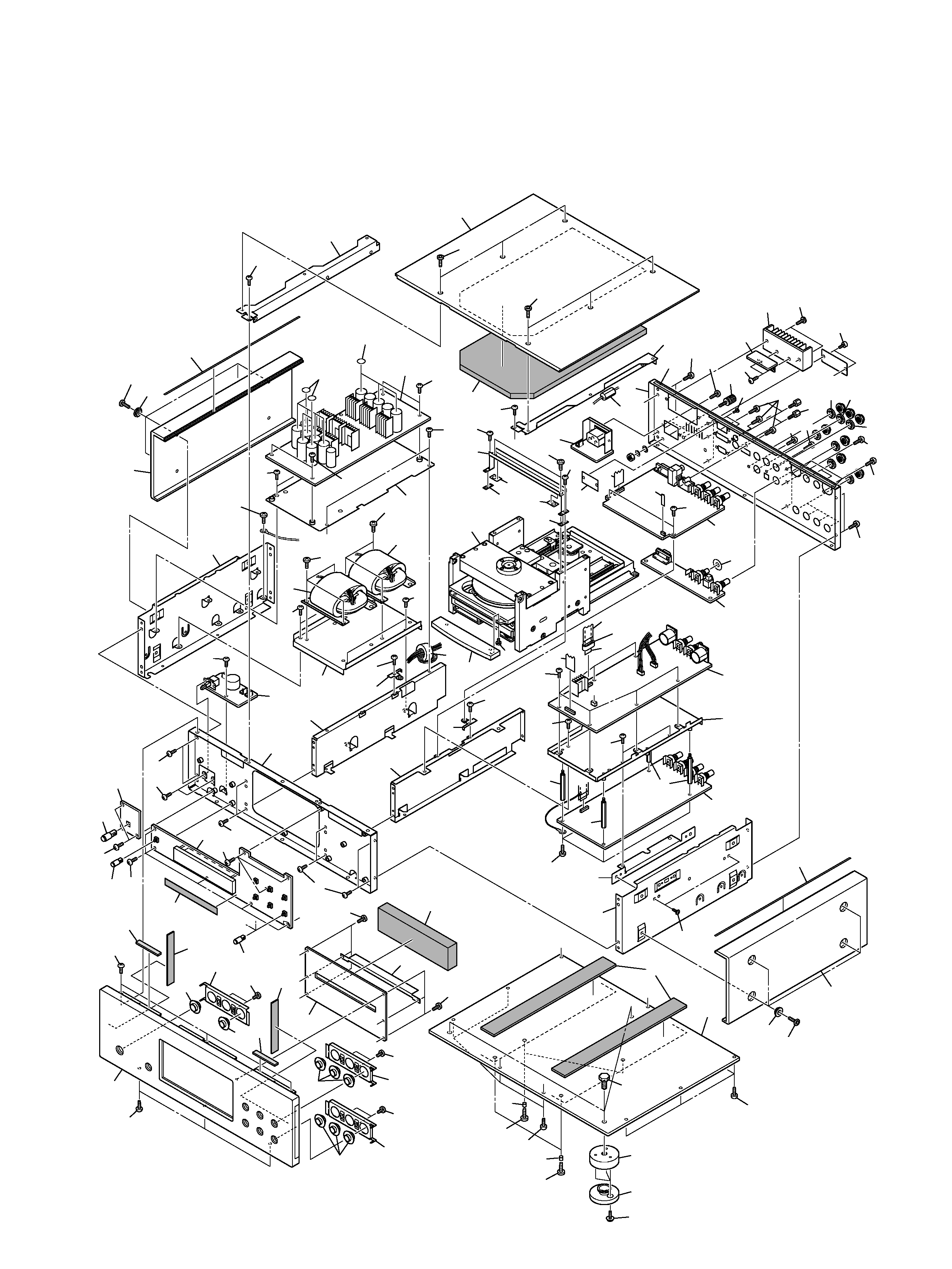
4 EXPLODED VIEWS AND PARTS LIST
EXPLODED VIEW-1
5
1
2
3
4
5
6
7
8
9
t
y
u
i
o
o
p
s
d
f
g
h
a
j
k
k
l
l
;
z
z
z
x
x
x
c
v
b
n
m
,
.
/
!
#
$
%
&
@
Q
^
W
E
*
(
T
T
)
Y
U
I
O
R
P
A
S
D
F
G
G
£ £
£
£
£
£
£
£
£
£
£
£
£
¢
¢
¡
¡
H
¡
TM
TM
TM
TM
TM
TM
TM
TM
§
§
§
¶
¶
·
·
·
ª
ª
º
´
oe
6
¡
¨
¨
®
TM
T
¨
0
w
w
q
e
r
¥
H
^
J
J
K
L
:
C
C
Z
X
A
A
B
B