±
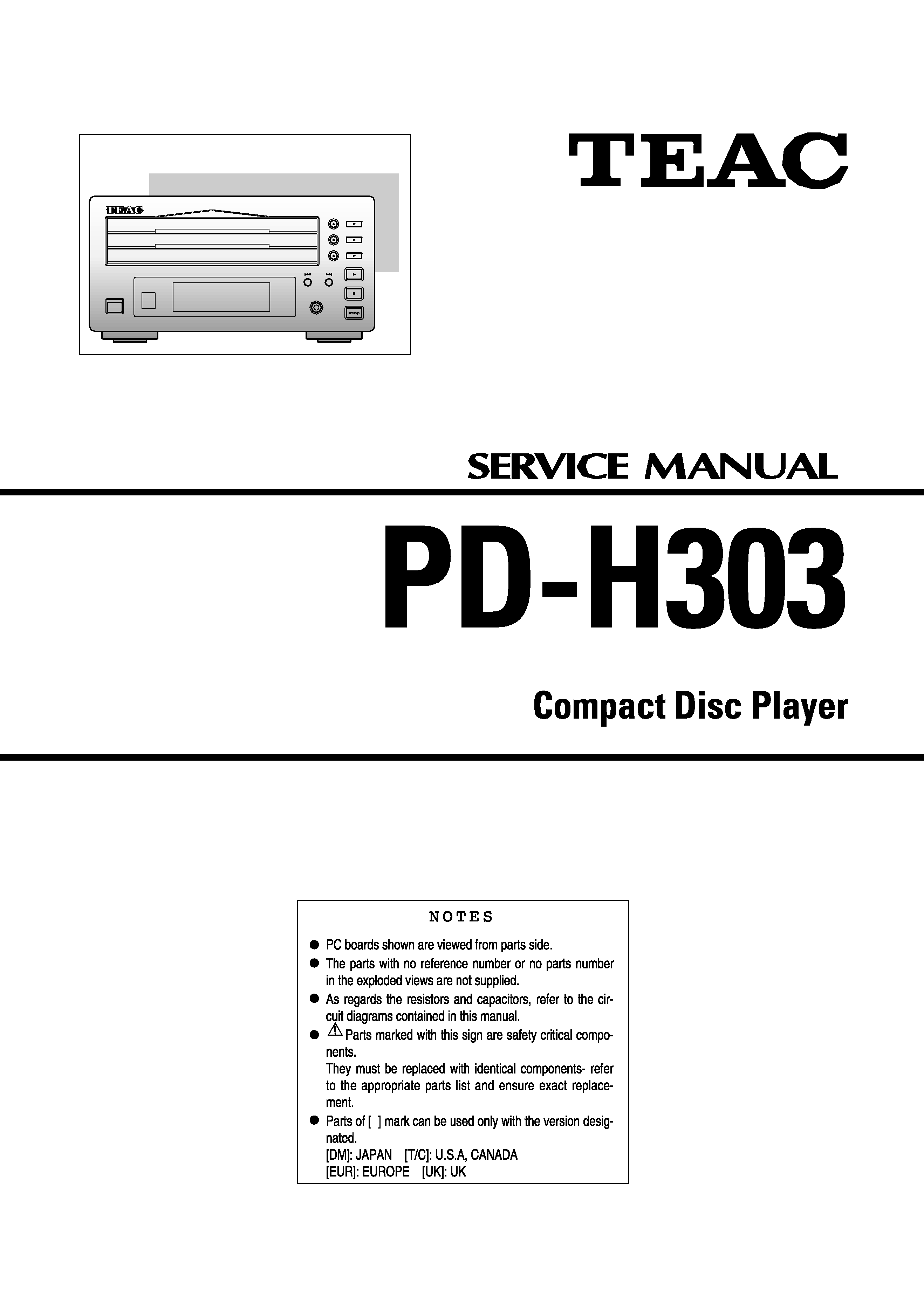
SERVICE MANUAL
3
TC9432AF/ TC9462AF (Digital Signal Processor)
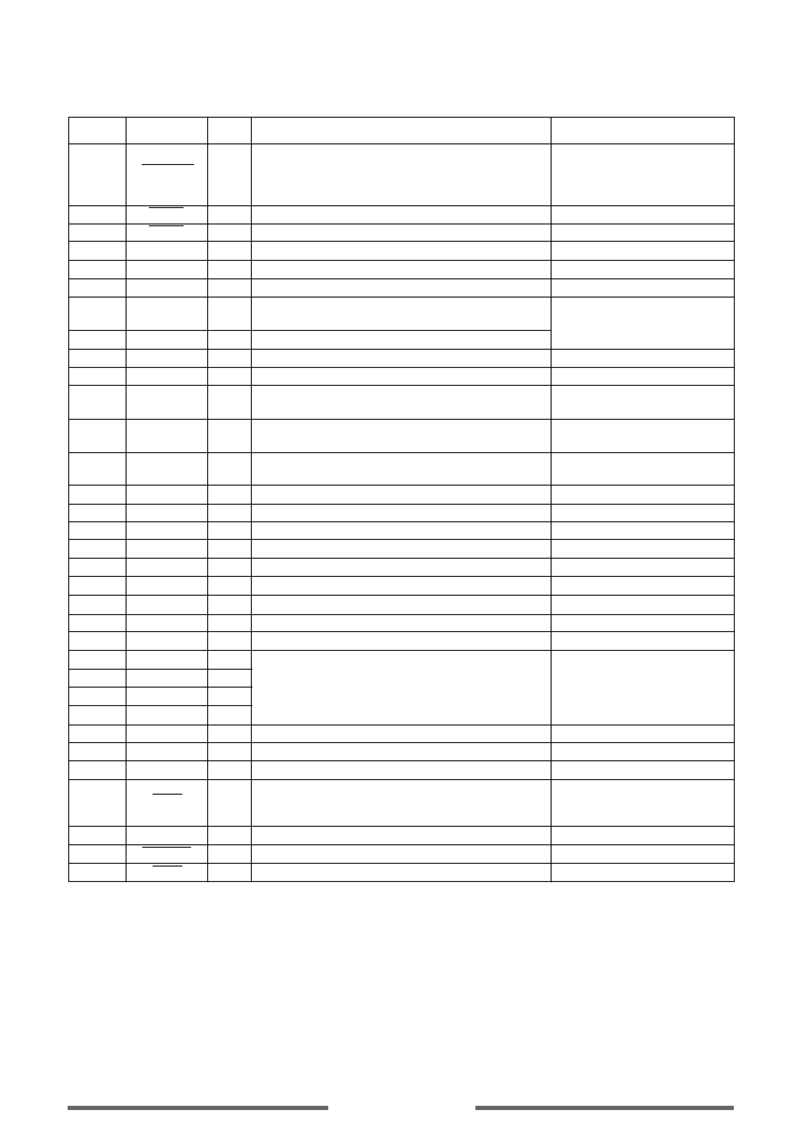
PIN No. NAME
I/O
FUNCTIONAL DESCRIPTION
REMARKS
TEST0
HSO
UHSO
EMPH
LRCK
VSS
BCK
AOUT
DOUT
MBOV
IPF
SBOK
CLCK
VDD
VSS
DATA
SFSY
SBSY
SPCK
SPDA
COFS
MONIT
VDD
TESIO0
P2VREF
HSSW
ZDET
PDO
TMAXS
TMAX
With pull-up resistor.
-
-
-
-
-
-
-
-
-
-
-
-
-
-
-
-
-
-
-
-
-
-
-
2-state output (PVREF,HiZ)
-
3-state output
(P2VREF,PVREF,VSS)
-
3-state output
(P2VREF,HiZ,VSS)
1
2
3
4
5
6
7
8
9
10
11
12
13
14
15
16
17
18
19
20
21
22
23
24
25
26
27
28
29
30
Test mode terminal. Normally, keep at open.
Playback speed mode flag output terminal.
Subcode Q data emphasis flag output terminal.
Emphasis ON at "H" level and OFF at "L" level.
The output polarity can invert by command.
Channel clock output terminal. (44.1 kHz)
L-ch at "L" level and R-ch at "H" level.
The output polarity can invert by command.
Digital GND terminal.
Bit clock output terminal. (1.4112 MHz)
Audio data output terminal.
Digital data output terminal.
Buffer memory over signal output terminal.
Over at "H" level.
Correction flag output terminal.
At "H " level, AOUT output is made to correction
impossibility by C2 correction processing.
Subcode Q data CRCC check adjusting result output
terminal. The adjusting result is OK at "H" level.
Subcode P~W data readout clock input/output termi-
nal. This terminal can select by command bit.
Digital power supply voltage terminal.
Digital GND terminal.
Subcode P~W data output terminal.
Playback frame sync signal output terminal.
Subcode block sync signal output terminal.
Processor status signal readout clock output terminal.
Processor status signal output terminal.
Correction frame clock output terminal. (7.35 kHz)
Internal signal (DSP internal flag and PLL clock) output
terminal. Selected by command.
Digital power supply voltage terminal.
Test input/output terminal. Normally, keep at "L" level.
PLL double reference voltage supply terminal.
2/4 times speed at "VREF" voltage.
1 bit DA converter zero detect flag output terminal.
Phase difference signal output terminal of EFM signal
and PLCK signal.
TMAX detection result output terminal. Selected by
command bit (TMPS).
TMAX detection result output terminal. Selected by
command bit (TMPS).
-
O
O
O
O
-
O
O
O
O
O
O
I/O
-
-
O
O
O
O
O
O
O
-
I
-
O
O
O
O
O
UHSO
HSO
PLAYBACK SPEED
H
H
Normal
H
L
2 times
L
H
4 times
L
L
-
DIFFERENCE RESULT
TMAX OUTPUT
Longer than fixed ferq.
"P2VREF"
Shorter than fixed freq.
"VSS"
Within the fixed freq.
"HiZ"
4
SERVICE MANUAL
PIN No. NAME
I/O
FUNCTIONAL DESCRIPTION
REMARKS
LPFN
LPFO
PVREF
VCOREF
VCOF
AVSS
SLCO
RFI
AVDD
RFCT
RFZI
RFRP
FEI
SBAD
TSIN
TEI
TEZI
FOO
TRO
VREF
RFGC
TEBC
TEBC
TEBC
DMO
2VREF
SEL
FLGA
FLGB
FLGC
FLGD
VDD
VSS
IO0
IO1
IO2
IO3
Analog input.
Analog output.
-
-
Analog output.
-
Analog output.
Analog input (Zin : selected by command)
-
Analog input (Zin : 50k
)
Analog input.
Analog input.
Analog input.
Analog input.
Analog input.
Analog input.
Analog input (Zin : 10k
)
Analog output (2VREF~AVSS)
-
3-state PWM signal output.
(2VREF, VREF, VSS)
(PWM carrier = 88.2 kHz)
3-state PWM signal
output.(2VREF, VREF, VSS)
-
-
-
-
-
-
-
-
-
31
32
33
34
35
36
37
38
39
40
41
42
43
44
45
46
47
48
49
50
51
52
53
54
55
56
57
58
59
60
61
62
63
64
65
66
67
LPF amplifier inverting input terminal for PLL.
LPF amplifier output terminal for PLL.
PLL reference voltage supply terminal.
VCO center frequency reference level terminal.
Normally, keep at "PVREF" level.
VCO filter terminal.
Analog GND terminal.
Data slice level output terminal.
RF signal input terminal.
Analog power supply voltage terminal.
RFRP signal center level input terminal.
RFRP zero cross input terminal.
RF ripple signal input terminal.
Focus error signal input terminal.
Sub-beam adder signal input terminal.
Test input terminal. Normally, keep at "VREF" level.
Tracking error signal input terminal.
Track in at tracking servo on.
Trcaking error zero cross input terminal.
Focus servo equalizer output terminal.
Tracking servo equalizer output terminal.
Analog reference voltage supply terminal.
RF amplitude adjustment control signal output terminal.
Tracking balance control signal output terminal.
Feed equalizer output terminal.
Speed error signal or feed search equalizer output ter-
minal.
Disk equalizer output terminal. (PWM carrier = 88.2 kHz
for DSP, Synchronize to PXO)
Analog double reference voltage supply terminal.
APC circuit ON/OFF indication signal output terminal.
At the laser on time, UHF = L at "HiZ" level and
UHF = H at "H" level.
Extemal flag output terminal for internal signal.
Can select signal from TEZC, FOON, FOK and RFZC by
command.
Extemal flag output terminal for internal signal.
Can select signal from DECT, FOON, FMON and RFZC
by command.
Extemal flag output terminal for internal signal.
Can select signal from TRON, TRSR, FOK and SRCH by
command.
Extemal flag output terminal for internal signal.
Can select signal from TRON, DMON, HYS and SHC by
command.
Digital power supply voltage terminal.
Digital GND terminal.
General I/O terminal. Can change over input port or
output port by command. At the input mode time can
readout a state of terminal (H/L) by read command. At
the output mode time can control a state of terminal
(H/L/HiZ) by command.
I
O
-
I
O
-
O
I
-
I
I
I
I
I
I
I
I
O
O
-
O
O
O
O
O
-
O
O
O
O
O
-
-
I/O
SERVICE MANUAL
5
PIN No. NAME
I/O
FUNCTIONAL DESCRIPTION
REMARKS
DMOUT
CKSE
DACT
TESIN
TESIO1
VSS
PXI
PXO
VDD
XVSS
XI
XO
XVDD
DVSR
RO
DVDD
DVR
LO
DVSL
TEST1
TEST2
TEST3
BUS0
BUS1
BUS2
BUS3
VDD
VSS
BUCK
CCE
TEST4
TSMOD
RST
With pull-up resistor.
With pull-up resistor.
With pull-up resistor.
Analog input.
Analog input.
-
-
-
-
-
-
-
-
-
-
-
-
-
With pull-up resistor.
With pull-up resistor.
With pull-up resistor.
Schmit input.
With pull-up resistor.
-
-
Schmit input.
Schmit input.
With pull-up resistor.
With pull-up resistor.
With pull-up resistor.
68
69
70
71
72
73
74
75
76
77
78
79
80
81
82
83
84
85
86
87
88
89
90
91
92
93
94
95
96
97
98
99
100
This terminal controls IO0~IO3 terminal.
At "L" level time, IO0, 1 out feed equalizer signal of
2-state PWM. IO2, 3 out disk equalizer signal of 2-state
PWM.
Normally, keep at open.
DAC test mode terminal. Normally, keep at open.
Test input terminal. Normally, keep at "L" level.
Test input/output terminal. Normally, keep at "L" level.
Digital GND terminal.
Crystal oscillator connecting input terminal for DSP.
Normally, keep at "L" level.
Crystal oscillator connecting output terminal for DSP.
Digital power supply voltage terminal.
Oscillator GND terminal for system clock.
Crystal oscillator connecting input terminal for system
clock.
Crystal oscillator connecting output terminal for sys-
tem clock.
Oscillator power supply voltage terminal for system
clock.
Analog GND terminal for DA converter. (R-ch)
R channel data forward output terminal.
Analog supply voltage terminal for DA converter.
Reference voltage terminal for DA converter.
L channel data forward output terminal.
Analog GND terminal for DA converter. (L-ch)
Test mode terminal. Normal, keep at open.
Test mode terminal. Normal, keep at open.
Test mode terminal. Normal, keep at open.
Micom interface data input/output terminal.
Digital Ppower supply voltage terminal.
Digital GND terminal.
Micom interface clock input terminal.
Command and data sending/receiving chip enable sig-
nal input terminal.
The bus
line becomes active at "L" level.
Test mode terminal. Normal, keep at open.
Local test mode selection terminal.
Reset signal input terminal. Reset at "L" level.
I
I
I
I
I
-
I
O
-
-
I
O
-
-
O
-
-
O
-
I
I
I
I/O
I/O
I/O
I/O
-
-
I
I
I
I
I