Ver 1.0 1999.04
MICROFILM
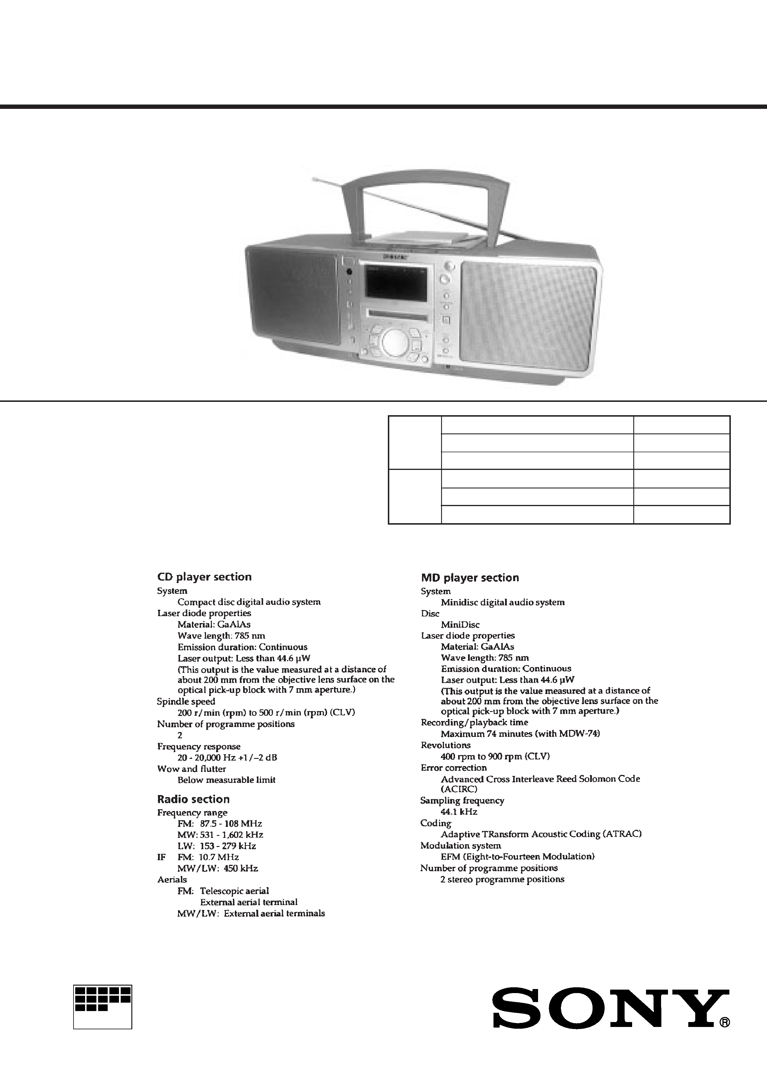
ZS-M50
SERVICE MANUAL
PERSONAL MINIDISC SYSTEM
SPECIFICATIONS
AEP Model
UK Model
Model Name Using Similar Mechanism
NEW
MD
MD Mechanism Type
MDM-3Z
Section
Optical Pick-up Type
KMS-260A
CD
Model Name Using Similar Mechanism
CFD-S27
Section
CD Mechanism Type
KSM-213CDM
Optical Pick-up Type
KSS-213C
Dolby noise reduction manufactured under license from
Dolby Laboratories Licensing Corporation.
"DOLBY" and the double-D symbol
a are trademarks of
Dolby Laboratories Licensing Corporation.
Continued on page 2
2
Specifications ........................................................................... 1
1. SERVICE NOTE ........................................................... 3
2. GENERAL ...................................................................... 5
3. DISASSEMBLY
3-1. Cabinet (Front) Sub ASSY,
Cabinet (Rear) Sub ASSY ......................................... 7
3-2. Control (L) Board ...................................................... 8
3-3. Control (R) Board ..................................................... 8
3-4. Control (F) Board, JOG Board .................................. 8
3-5. BATT Board .............................................................. 9
3-6. Power Board .............................................................. 9
3-7. Tuner Board, Antenna SW Board ............................. 9
3-8. Center Block Section .............................................. 10
3-9. Cabinet (Upper), Chassis (Main) ............................ 10
3-10. Optical Pick-up ASSY, CD Motor Board ................. 11
3-11. Control SW Board .................................................... 11
3-12. Motor Board, Belt, Motor (M703) ........................... 11
3-13. LCD Board, BL Board ............................................ 12
3-14. Audio Board ............................................................ 12
3-15. Line Board ............................................................... 13
3-16. Main Board ............................................................. 13
3-17. MD Block ASSY ..................................................... 14
3-18. DG Board ................................................................ 14
3-19. Chassis (MD) .......................................................... 15
3-20. BD Board ................................................................ 15
3-21. Sub Chassis ASSY, MD Mechanism Deck ............. 16
3-22. Shutter ASSY .......................................................... 16
3-23. SW Board ................................................................ 17
3-24. "Head, Over Write", Slider ASSY .......................... 17
3-25. MD Optical Pick-up Block ..................................... 18
4. TEST MODE
4-1. Caution When Using the Test Mode ......................... 19
4-2. Test Mode Settings ................................................... 19
4-3. Releasing the Test Mode ........................................... 19
4-4. Basic Operations of the Test Mode ........................... 19
4-5. Selecting the Test Mode ............................................ 19
4-6. Functions of Other Buttons ...................................... 20
4-7. Test Mode Display .................................................... 20
TABLE OF CONTENTS
5. ADJUSTMENTS
MD Section ...................................................................... 21
CD Section ....................................................................... 24
Display Section ................................................................ 25
Tuner Section ................................................................... 26
6. DIAGRAMS
6-1. Explanation of IC Terminals ................................... 28
6-2. Block Diagram (Main Section) ............................... 35
6-3. Block Diagram (MD Section) ................................. 39
6-4. Printed Wiring Boards Main Section ................. 43
6-5. Schematic Diagram Main Section (1/3) ............. 47
6-6. Schematic Diagram Main Section (2/3) ............. 51
6-7. Schematic Diagram Main Section (3/3) ............. 55
6-8. Printed Wiring Boards Audio Section ................ 58
6-9. Schematic Diagram Audio Section .................... 61
6-10. Schematic Diagram DG Section ........................ 66
6-11. Printed Wiring Boards DG Section .................... 71
6-12. Printed Wiring Boards Tuner Section ................ 73
6-13. Schematic Diagram Tuner Section ..................... 75
6-14. Schematic Diagram Control Section .................. 78
6-15. Printed Wiring Boards Control Section ............. 81
6-16. Printed Wiring Boards BD Section .................... 83
6-17. Schematic Diagram BD Section ........................ 85
7. EXPLODED VIEWS
7-1. Rear Cabinet Section ................................................ 95
7-2. Front Cabinet Section ............................................... 96
7-3. Center Block Section ................................................ 97
7-4. Upper Cabinet Section .............................................. 98
7-5. MD Section (1) ......................................................... 99
7-6. MD Section (2) ....................................................... 100
7-7. CD Optical Pick-up Section ................................... 101
8. ELECTRICAL PARTS LIST ................................. 102
3
NOTES ON HANDLING THE OPTICAL PICK-UP BLOCK
OR BASE UNIT
The laser diode in the optical pick-up block may suffer electrostatic
breakdown because of the potential difference generated by the
charged electrostatic load, etc. on clothing and the human body.
During repair, pay attention to electrostatic breakdown and also use
the procedure in the printed matter which is included in the repair
parts.
The flexible board is easily damaged and should be handled with
care.
NOTES ON LASER DIODE EMISSION CHECK
The laser beam on this model is concentrated so as to be focused on
the disc reflective surface by the objective lens in the optical pick-
up block. Therefore, when checking the laser diode emission, ob-
serve more than 30 cm away from the objective lens.
LASER DIODE AND FOCUS SEARCH OPERATION
CHECK
1. Close the lid for CD.
2. Press CD
fl button.
3. Confirm the laser diode emission while observing the objecting
lens. When there is no emission, Auto Power Control circuit or
Optical Pick-up is broken.
Objective lens moves up and down once for the focus search.
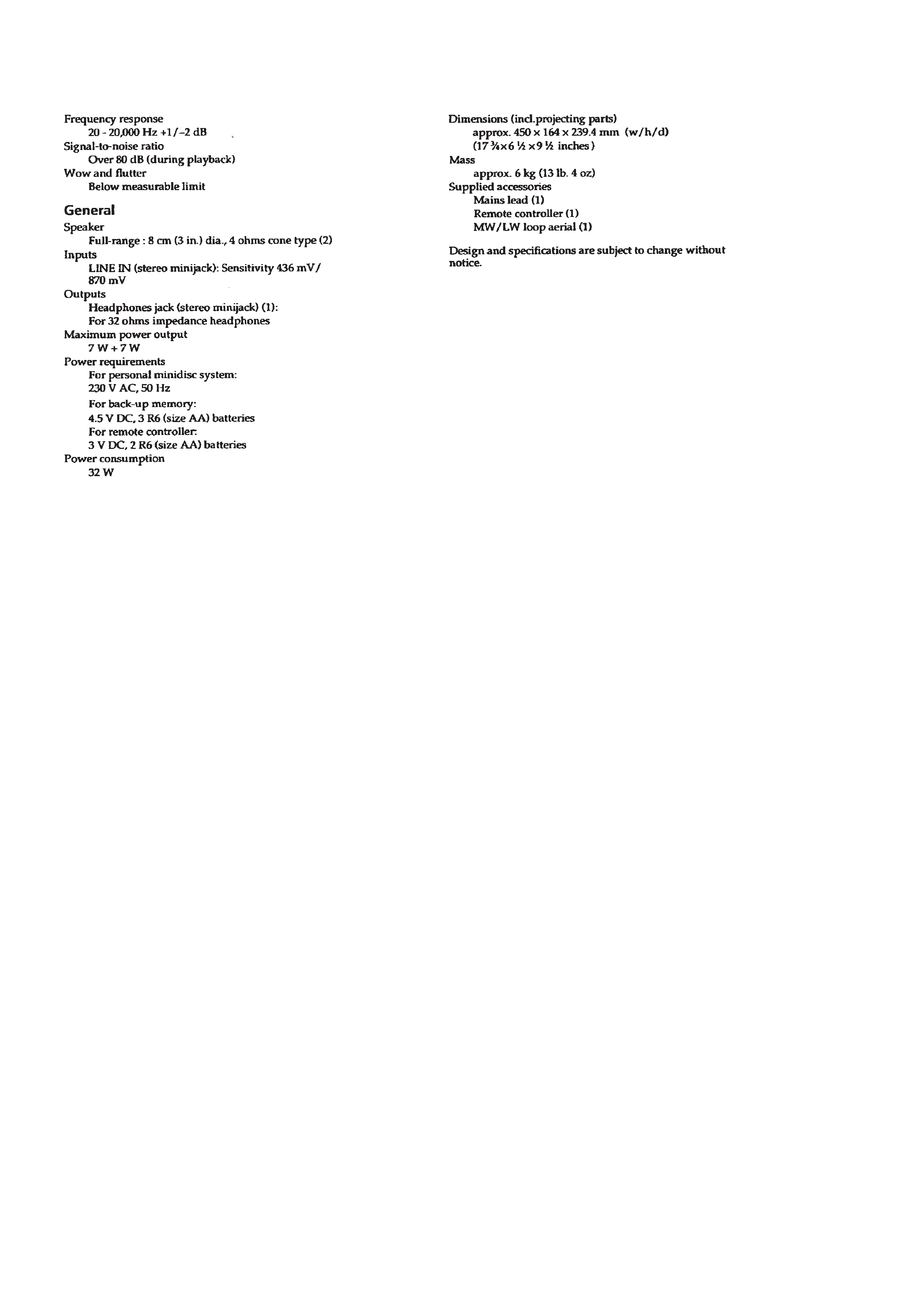
CAUTION DURING WHEN MOUNTING THE PULLEY
FOR THE CD DOOR MOTOR (M703)
Make the following adjustment when mounting the CD door motor
(part number : 1-763-224-11) and motor pulley (part number : 2-
627-174-01) of the CD section.
Specification : A = 0.9 to 1.1mm
SECTION 1
SERVICE NOTE
SAFETY-RELATED COMPONENT WARNING!!
COMPONENTS IDENTIFIED BY MARK
! OR DOTTED LINE WITH
MARK
!ON THE SCHEMATIC DIAGRAMS AND IN THE PARTS
LIST ARE CRITICAL TO SAFE OPERATION.
REPLACE THESE COMPONENTS WITH SONY PARTS WHOSE
PART NUMBERS APPEAR AS SHOWN IN THIS MANUAL OR IN
SUPPLEMENTS PUBLISHED BY SONY.
Flexible Circuit Board Repairing
· Keep the temperature of the soldering iron around 270°C during
repairing.
· Do not touch the soldering iron on the same conductor of the
circuit board (within 3 times).
· Be careful not to apply force on the conductor when soldering or
unsoldering.
Notes on chip component replacement
· Never reuse a disconnected chip component.
· Notice that the minus side of a tantalum capacitor may be dam-
aged by heat.
CHUCK PLATE JIG ON REPAIRING
On repairing CD section, playing a disc without the CD lid, use
Chuck Plate Jig.
· Code number of Chuck Plate Jig : X-4918-255-1
4
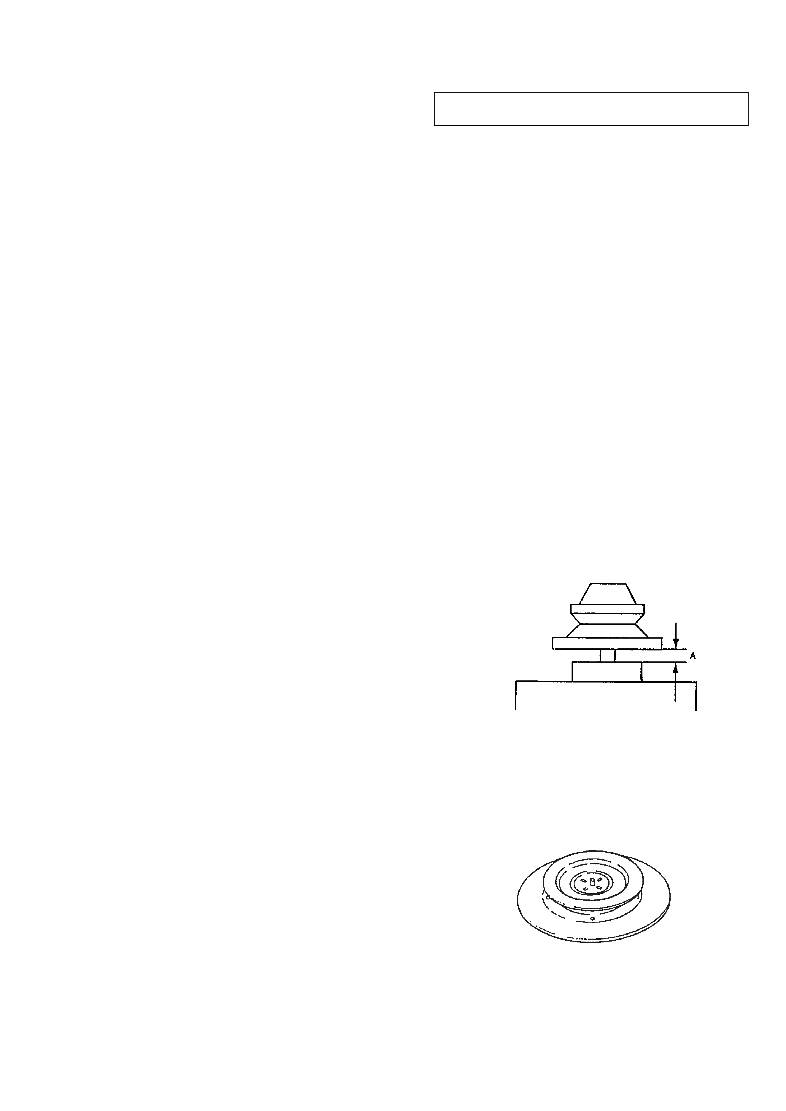
ABOUT THE BD BOARD WAVEFORM CHECKING JIG
The special jig (J-2501-124-A) is highly convenient when check-
ing the waveform of the BD board of the MD section. Pin names
and items to check are as follows:
I+3V : for IOP measurement (check for depleted optical pickup
laser)
IOP
: for IOP measurement (check for depleted optical pickup
laser)
TEO : TRK error signal (traverse adjustment)
VC
: Standard level for checking signals
RF
: RF signal (jitter check)
BD board
CN110
DG board
I + 3V
IOP
TEO
VC
RF
Jig
(J-2501-124-A)
MD block section
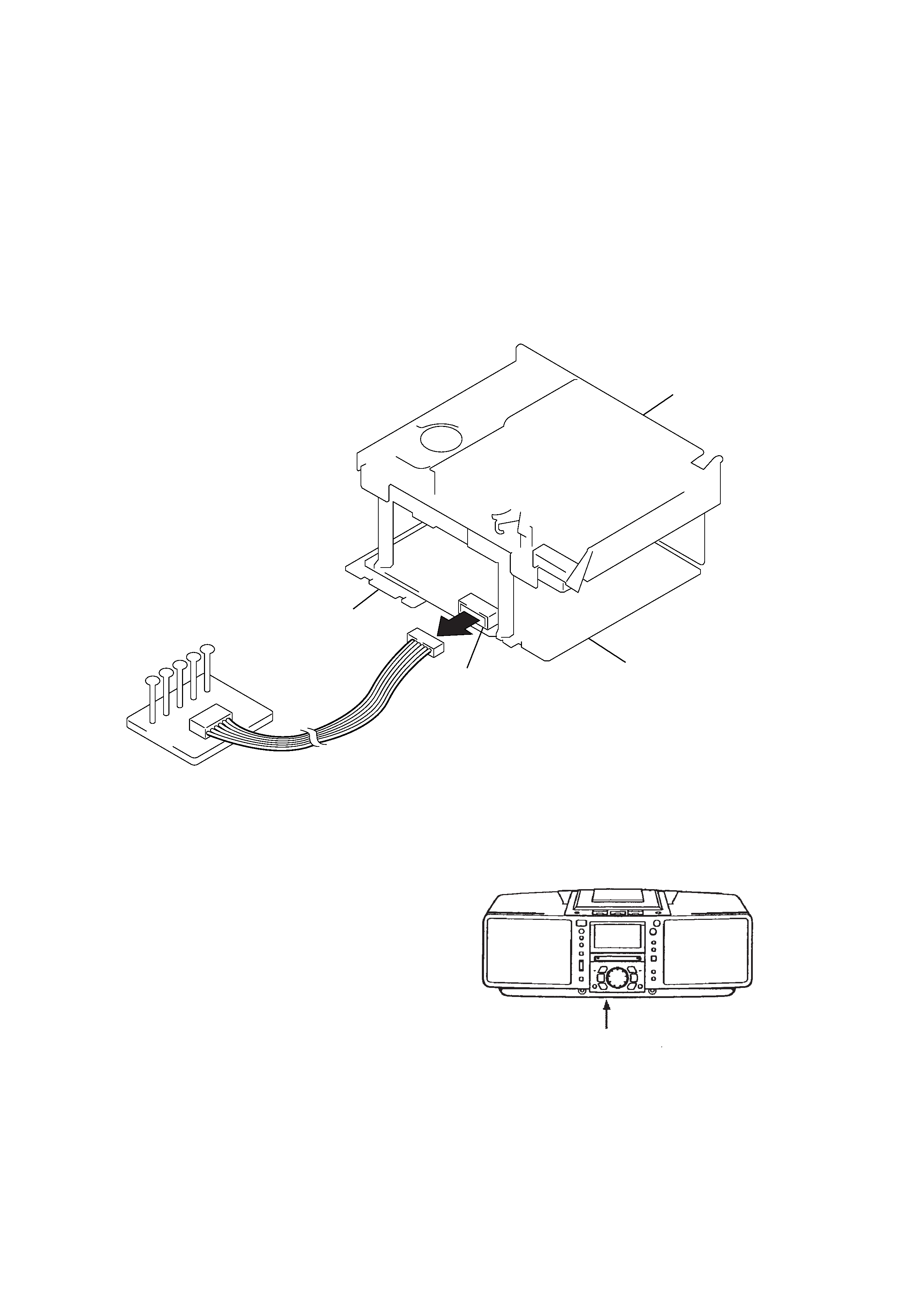
ABOUT THE HARDWARE RESET
It is possible to reset the system microcomputer by pressing the
RESET button located on the bottom with a pointed object. Use
this button when the unit cannot be operated properly due to such
problems as microcomputer errors, etc.
RESET button
(Located on the bottom)
5
SECTION 2
GENERAL
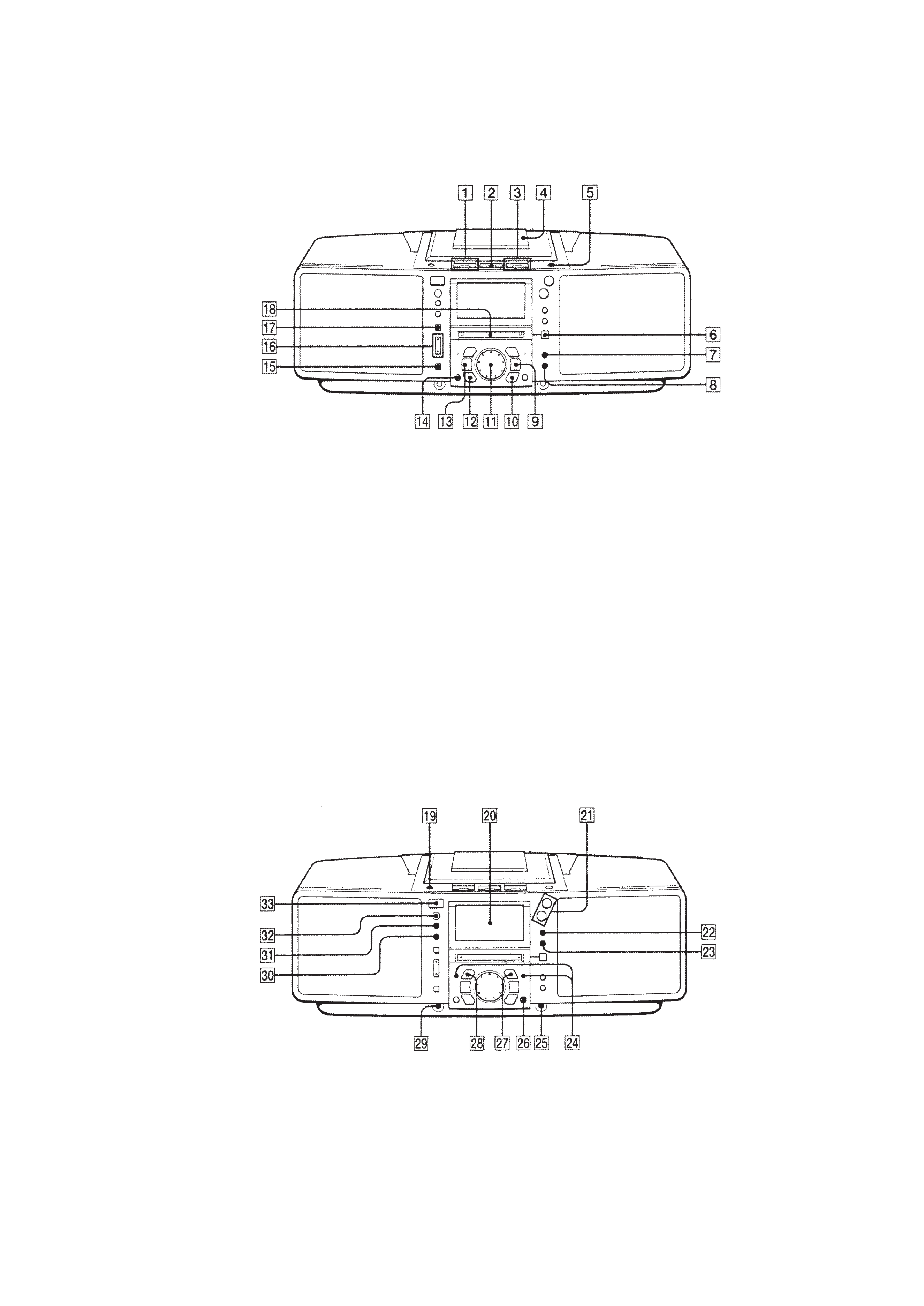
LOCATION AND FUNCTION OF CONTROLS
1 MD operation buttons
fl (play/pause)
(stop)
2 BAND button
3 CD operation buttons
fl (play/pause)
(stop)
4 CD lid
5 6 CD OPEN/CLOSE button
6 6 MD EJECT button
7 MONO/ST, REPEAT button
8 AUTO PRESET/RDS/SHUF/PGM button
9 TUNE +, ÷, ) button
!º YES, ENTER button
!¡ Jog dial
=/+ AMS
PRESET
!TM NO, CANCEL button
!£ TUNE , ¿, 0 button
!¢ EDIT button
! REC button
!§ REC IT button
TO TOP, TO END
!¶ SYNCHRO REC
CD
" MD button
!· MD insert section
!ª LINE/LINE LEVEL button
@º Display window
@¡ VOLUME +, buttons
@TM BASS/TREBLE button
@£ MEGA BASS button
@¢ Jog dial Function indicator
AMS/PRESET SELECT
@ LINE IN terminal
@§ DISPLAY button
@¶ INSERT/TIMER button
@· DELETE/CLOCK button
@ª 2 (Headphones) Jack (stereo mini jack)
#º STANDBY button
#¡ SLEEP button
#TM Remote control receiver section
#£ OPERATE button
FRONT PANEL: MD/CD/RADIO Section
FRONT PANEL: TIMER, COM Section