SERVICE MANUAL
XM SATELLITE RADIO RECEIVER
US Model
SPECIFICATIONS
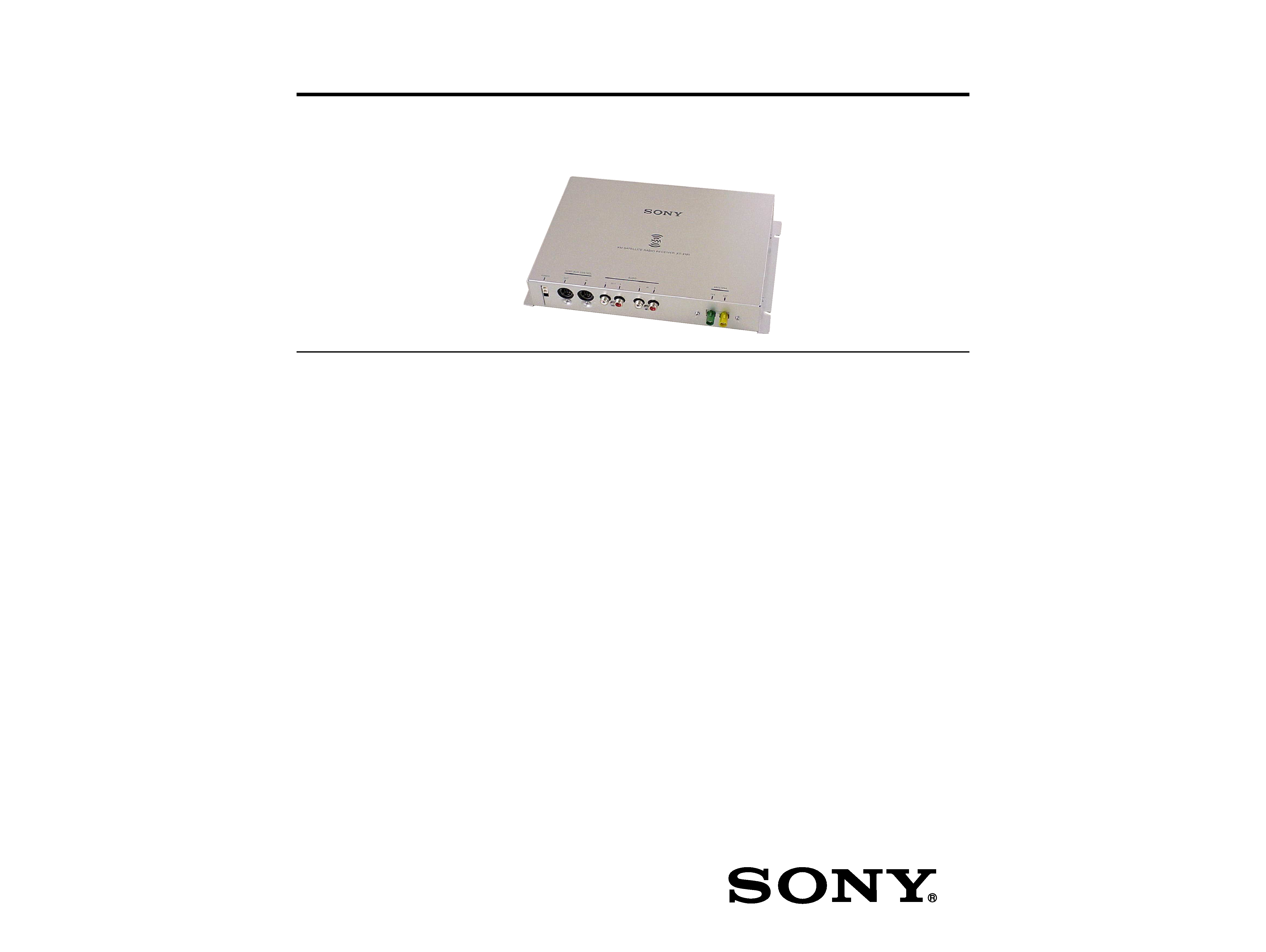
XT-XM1
Ver 1.1 2003.06
9-874-057-02
Sony Corporation
2003F05-1
e Vehicle Company
C
2003.06
Published by Sony Engineering Corporation
Notes on chip component replacement
·Never reuse a disconnected chip component.
· Notice that the minus side of a tantalum capacitor may be dam-
aged by heat.
Frequency
2332.5 2345.0 MHz
Power requirements
12 V DC car battery
(negative ground)
Outputs
BUS control output
Audio output
Inputs
Antenna input (Satellite,
Terrestrial)
BUS control input
Audio input
Dimensions
224
× 37.8 × 160 mm
(8 7/8 × 1 1/2 × 6 3/8 in.)
(w/h/d)
Mass
Approx. 1.0 kg
(2 lb. 4 oz.)
Supplied accessories
Parts for installation and
connection (1 set)
Design and specifications are subject to change
without notice.
2
XT-XM1
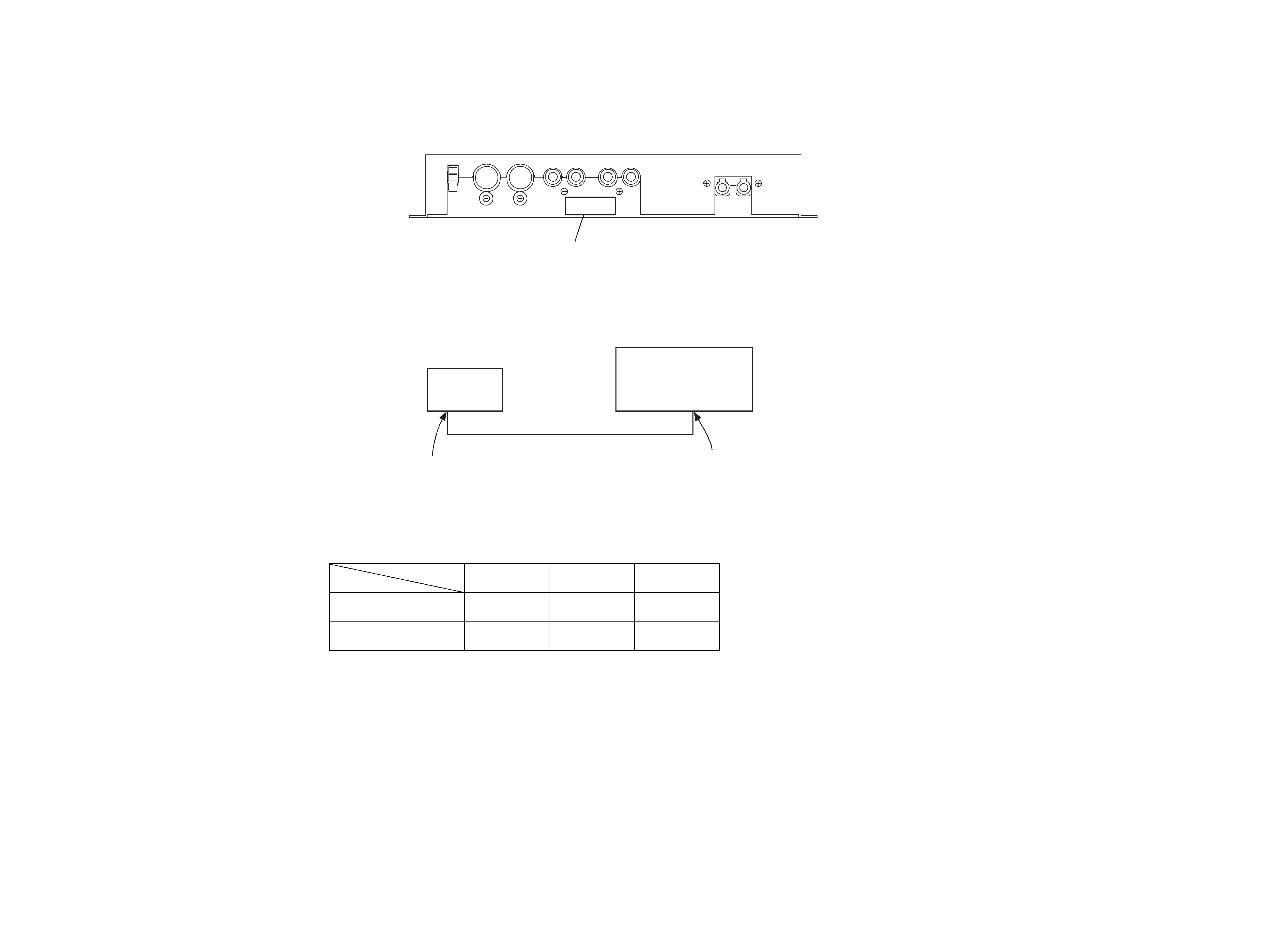
POSITION OF THE ID LABEL
The ID label is stuck on the following position.
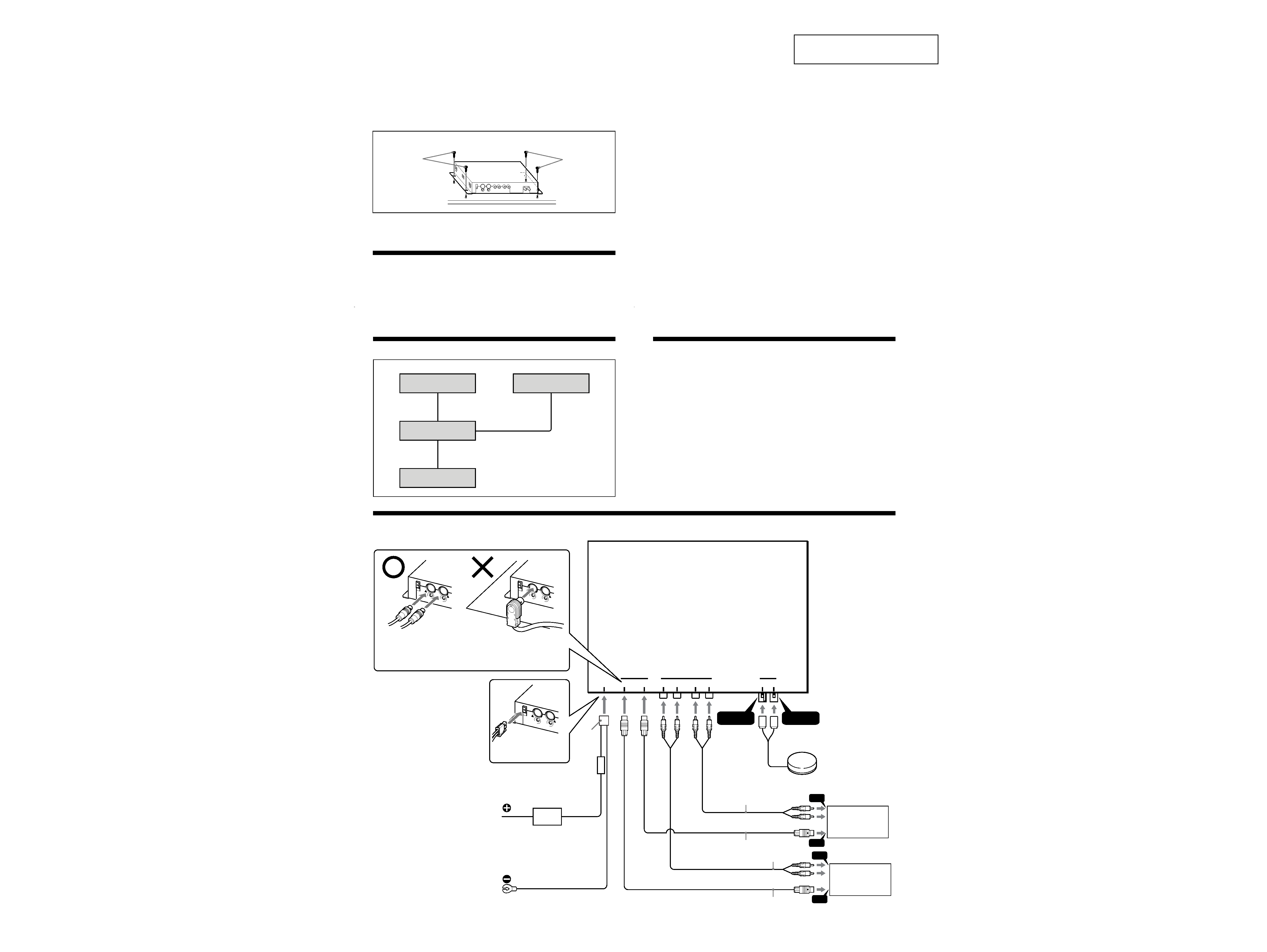
ABOUT THE MASTER UNIT
This unit is compatible only with the master unit (car audio system compatible with SONY BUS SYSTEM) released year 2000 or after.
Connect the master unit as shown below to activate this unit.
ABOUT TYPE A/B
IC107 of the TRANSLATOR board has been changed in the midway the production.
Part No. of the TRANSLATOR board and instruction manual have been also changed accompanying the above change.
When you repair or replace parts indicated in the table, please be sure to check the serial No..
TRANSLATOR
IC701
Instruction
board
manual
TYPE A
A-3274-400-A
6-801-746-02
3-243-168-12
(Serial No. 128500 or before)
MN101C49GYB1
TYPE B
A-3274-779-A
6-801-453-01
3-243-168-21
(Serial No. 128501 or after)
MN101C49GYG
XT-XM1
master unit
released in year 2000 or after
(compatible with
SONY BUS SYSTEM)
SONY BUS CONTROL OUT
SONY BUS CONTROL IN
SECTION 1
SERVICING NOTES
ID label
SIDE VIEW
Ver 1.1
3
XT-XM1
SECTION 2
GENERAL
This section is extracted from
instruction manual.
Connection
Connectionexample
Cautions
· This unit is designed for negative ground 12 V DC operation only.
· Before making connections, turn the car ignition off to avoid short circuits.
· Connect the yellow power input cord only after all other cords have been connected.
· Run all ground leads to a common ground point.
Connectiondiagram
XM Antenna*
Sony BUS Compatible
Car Audio*
XT-XM1
CD/MD changer*
* not supplied
POWER
SONY BUS CONTROL
OUT
IN
L
R
L
R
OUT
IN
AUDIO
TER
SAT
ANTENNA
Yellow
To a +12 V power terminal which
is energized at all times
Be sure to connect the black ground
lead to it first.
Fuse (3 A)
Black
To a metal point on the car
First connect the black ground lead,
then connect the yellow power input
leads.
CD/MD changer
(not supplied)
Sony BUS Compatible
Car Audio
(not supplied)
4
3
XM antenna
(not supplied)
OUT
OUT
IN
IN
Green
Yellow
Connect as the connector
hook facing down
Connect with BUS cable to
the XM Satellite receiver,
aligning the v marks.
RCA pin cord
(not supplied)
BUS cable
(not supplied)
2
Note
When you use an optional BUS cable, note
that a BUS cable with an 8-pin plug (L-type)
cannot be used because of its shape.
(Curry)
Installingthe unit
·Mount the unit either inside the trunk or under a seat.
·Choose the mounting location carefully so the unit will not interfere with the normal movements of
the driver and it will not be exposed to direct sunlight or hot air from the heater.
·Do not install the unit under the floor carpet, where the heat dissipation from the unit will be
considerably impaired.
First, place the unit where you plan to install it, and mark the positions of the four screw holes on
the mounting surface.
Notes
· Use only the supplied screws.
· Be sure not to damage the fuel tank or brake line with the tapping screws.
Fuse replacement
If the fuse blows, check the power connection and replace the fuse. If the fuse blows again after
replacement, there may be an internal malfunction.
Warning
Use a fuse with the specified amperage rating.
Use of a higher amperage fuse may cause serious damage.
Screw hole:
ø3.3 mm (5/32 in.)
1
1
4
XT-XM1
SECTION 3
DIAGRAMS
Note on Printed Wiring Board:
· X : parts extracted from the component side.
· Y : parts extracted from the conductor side.
·
: Pattern from the side which enables seeing.
(The other layers' patterns are not indicated.)
3-1.
NOTE FOR PRINTED WIRING BOARD AND SCHEMATIC DIAGRAM
Note on Schematic Diagram:
· All capacitors are in µF unless otherwise noted. pF: µµF
50 WV or less are not indicated except for electrolytics
and tantalums.
· All resistors are in and 1/4 W or less unless otherwise
specified.
· C : panel designation.
· A : B+ Line.
·Power voltage is dc 14.4V and fed with regulated dc power
supply from BATT cords.
·Voltages and waveforms are dc with respect to ground
under no-signal (detuned) and master unit connected
conditions.
no mark : XM
·Voltages are taken with a VOM (Input impedance 10 M).
Voltage variations may be noted due to normal produc-
tion tolerances.
·Waveforms are taken with a oscilloscope.
Voltage variations may be noted due to normal produc-
tion tolerances.
· Circled numbers refer to waveforms.
· Signal path.
F
: XM
E
: AUDIO (AUX)
Caution:
Pattern face side:
Parts on the pattern face side seen from
(Conductor Side)
the pattern face are indicated.
Parts face side:
Parts on the parts face side seen from
(Component Side) the parts face are indicated.
XT-XM1
5
5
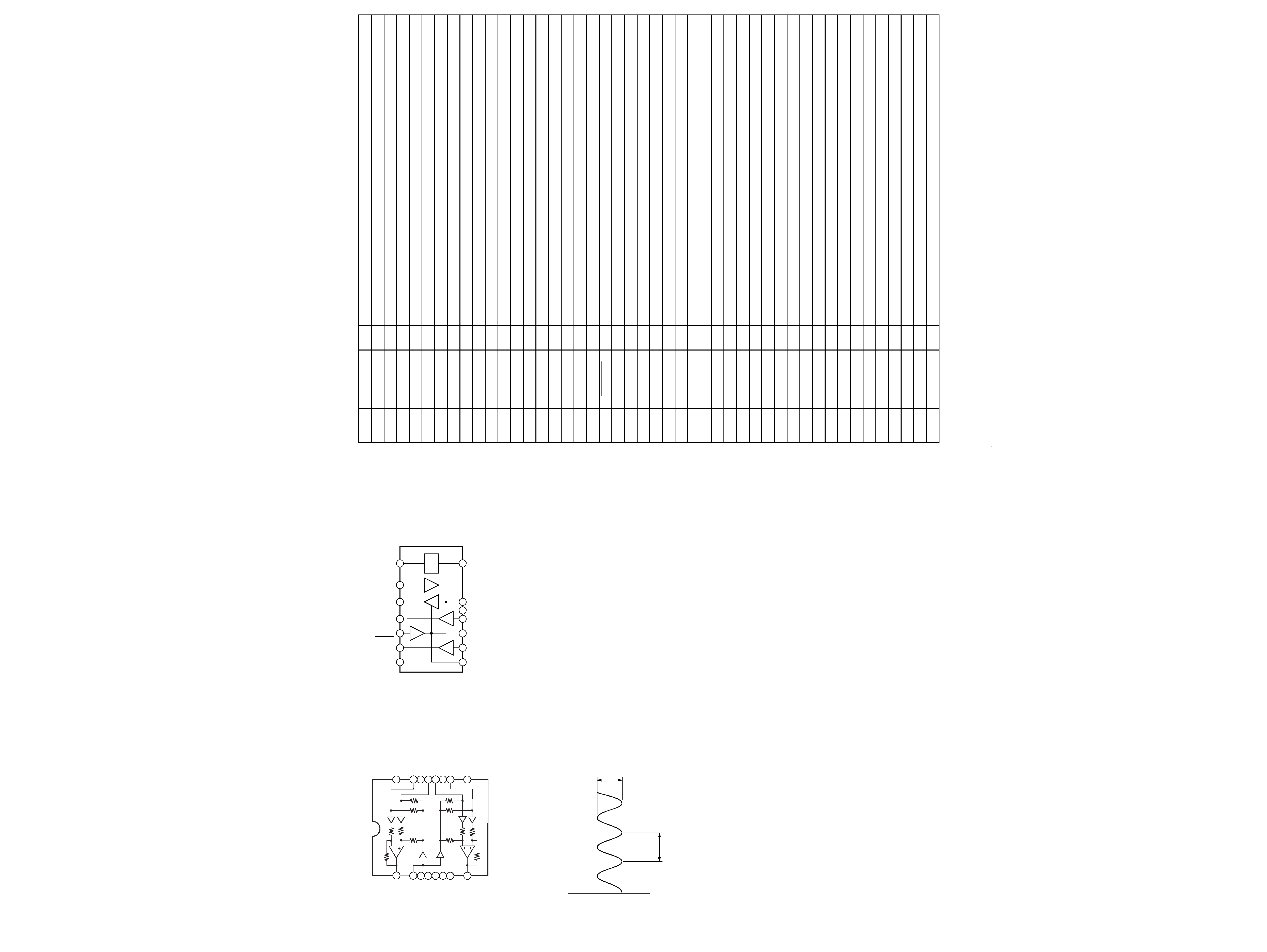
· IC Block Diagrams
IC103
TA2050F (EL)
IC106
BA8272FV-E2
1
2
3
4
5
6
7
8
9
10
11
12
13
14
15
16 NC
IN()1
IN(+)1
IN(+)2
IN()2
NC
NC
NC
OUT1
VREF
NC
GND
NC
VCC
NC
OUT2
1
2
3
4
5
6
7
8
9
10
14
13
12
11
VCC
BUS
ON
LINK
OFF
CLK
OUT
DATA
OUT
DATA
IN
BUS
RESET
BUS
DATA
VREF
BUS
CLK
GND
BUS
ON
IN
BUS
ON
OUT
RESET
RESET
SWITCH
· Waveform
1
IC107 qs (OSC2)
2.7 Vp-p
54 ns
3-2.
IC PIN FUNCTION DESCRIPTION
· IC107 MN101C49GYB1 (SYSTEM CONTROLLER)
Pin No.
Pin Name
I/O
Description
1VREF
I
Reference voltage (0V) input terminal (for A/D converter)
2
FLASH
I
Internal flash memory data write mode detection signal input terminal
"L": data write mode
3 to 9
(IN-L)
I
Not used
10
VREF+
I
Reference voltage (+5V) input terminal (for A/D converter)
11
VDD
--
Power supply terminal (+5V)
12
OSC2
OMain system clock output terminal (18.432 MHz)
13
OSC1
IMain system clock input terminal (18.432 MHz)
14
VSS
--
Ground terminal
15
XI (VSS)
I
Sub system clock input terminal
Not used
16
XO
O
Sub system clock output terminal
Not used
17
MMOD (VSS)
I
Memory mode selection signal input terminal
Not used
18
TX
O
IS bus "TXRX" signal output terminal
19
RX
I
IS bus "TXRX" signal input terminal
20
IS FOUT
O
IS bus "FRAME" signal output terminal
21
SO
O
Serial data output to the SONY bus interface
22
SI
I
Serial data input from the SONY bus interface
23
SCLK
O
Serial clock signal output to the SONY bus interface
24
GND
--
Ground terminal
25
LINKOFF
O
Bus on/off control signal output
"L": bus on
26
BUSON
I
Bus on/off control signal input from the SONY bus interface
"H": bus on
27
(IN-L)
I
Not used
28
BU IN
I
Battery detection signal input terminal
"L" is input at low voltage
29
IS FIN
I
IS bus "FRAME" signal input terminal
30, 31
(IN-L)
I
Not used
32
VDD2
--
Power supply terminal (+5V)
33
X T RESET
I
System reset signal input from the reset signal generator
"L": reset
"L" is input for several 100 msec after power on, then it changes to "H"
34 to 40
(IN-L)
I
Not used
41
VPP
--
Power supply terminal (+5V)
42
PC-TX
O
Not used
43
PC-RX
I
Not used
44
NC
--
Not used
45
E2PROM-SCL
O
Serial data transfer clock signal output to the EEPROM
46
NC
--
Not used
47
E2PROM-SDA
I/O
Two-way data bus with the EEPROM
48 to 62
NC
--
Not used
63
X M-RESET
O
Reset signal output to the MAIN board
"L": reset
64
X M-STANDBY
O
Standby signal output to the MAIN board
"L": standby
65
P-ON
O
+9V power supply on/off control signal output
"H": power on
66
SELECT (H-XM)
O
Relay drive signal output
"H": XM on
67
X MUTE
O
Muting on/off control signal output
"L": muting on
68 to 94
NC
--
Not used
95
DAVSS
--
Ground terminal (for D/A converter)
96to 99
NC
--
Not used
100
DAVDD
--
Power supply terminal (+5V) (for D/A converter)