1
SERVICE MANUAL
AEP Model
UK Model
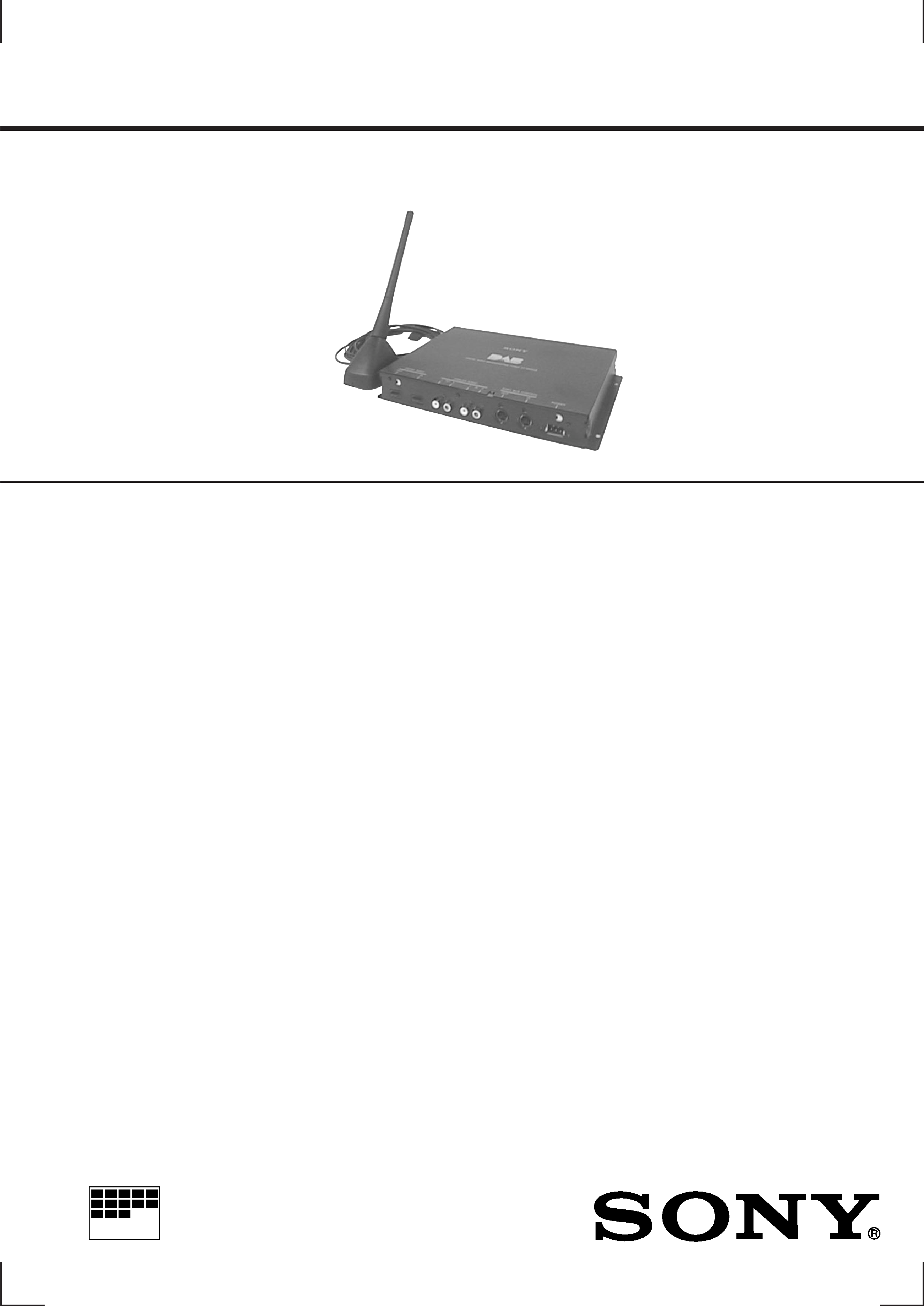
XT-100DAB
DIGITAL AUDIO
BROADCASTING TUNER
Frequency
174.928 - 239.200 MHz
(Band III)
1452.960 - 1490.624 MHz
(L band)
Mode
Mode I (Band III)
Mode II (L band)
Power requirements
12 V DC car battery
(negative earth)
Outputs
BUS control output
Audio optical output
Audio output
Inputs
Aerial input
BUS control input
Audio optical input
Audio input
Dimensions
240
× 35 × 163 mm
(w/h/d)
Mass
Approx. 1.2 kg
Supplied accessories
Parts for installation and
connection (1 set)
DAB aerial (1)
BUS cable (1)
RCA pin cord (1)
Optical cable (1)
Design and specifications are subject to change without
notice.
SPECIFICATIONS
MICROFILM

2
TABLE OF CONTENTS
1. SERVICE NOTE ................................................................ 2
2. GENERAL
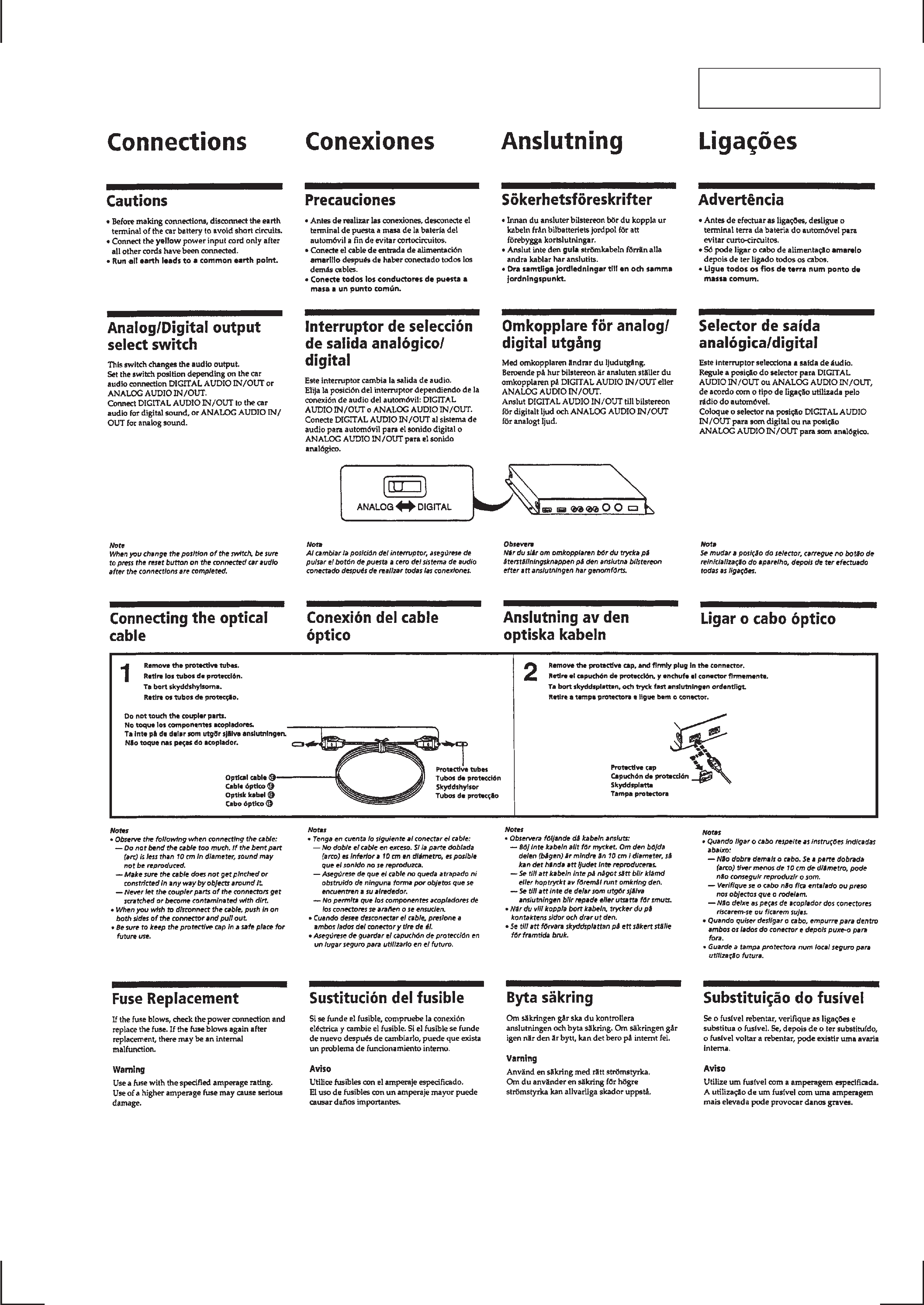
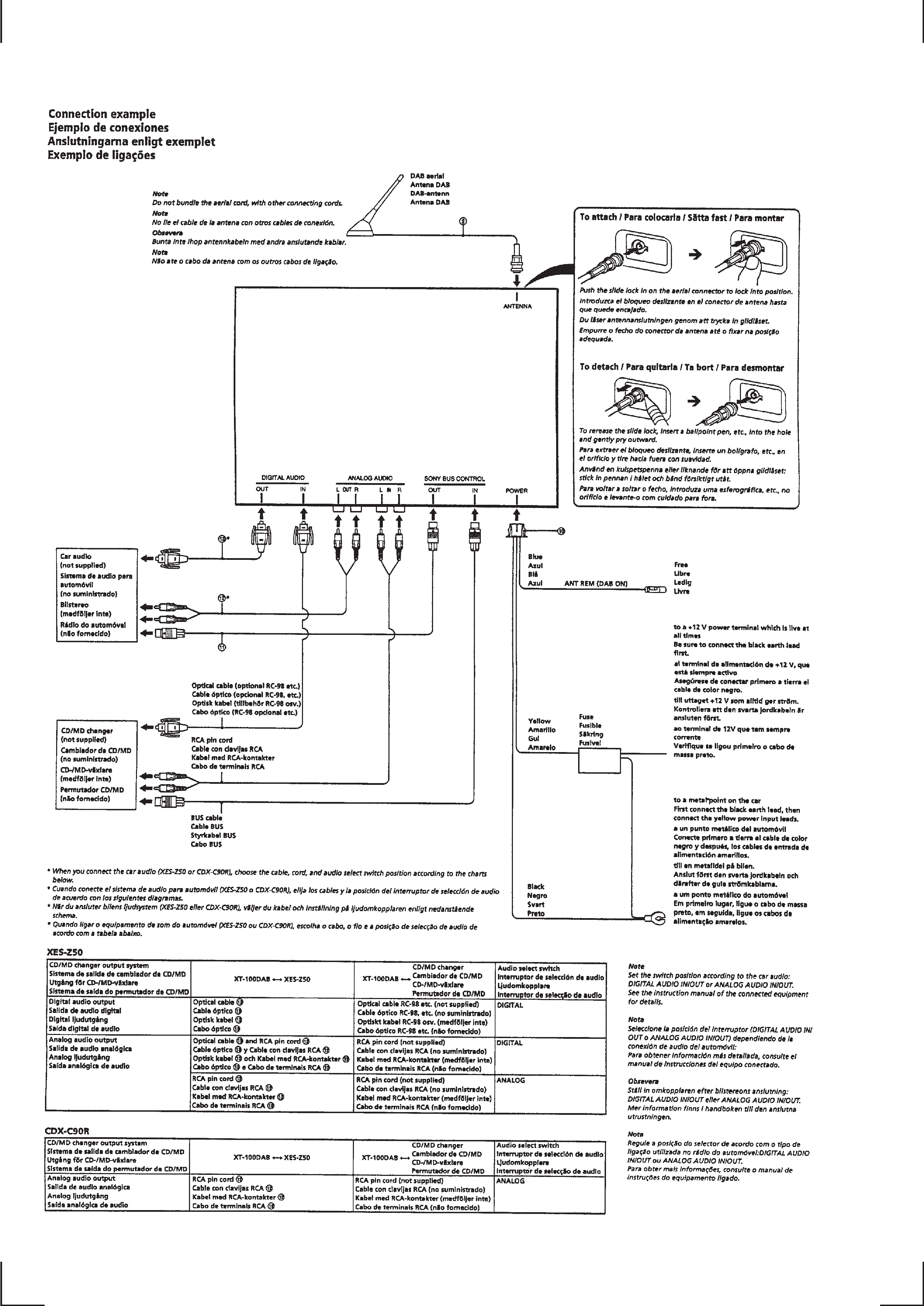
Connections ............................................................................. 3
3. ELECTRICAL ADJUSTMENTS ............................... 5
4. DIAGRAMS
4-1. Block Diagram RF Section ............................................. 7
4-2. Block Diagram Audio Section ........................................ 9
4-3. IC Pin Descriptions ........................................................... 11
4-4. Printed Wiring Board ........................................................ 21
4-5. Schematic Diagram Main Board (1/4) .......................... 25
4-6. Schematic Diagram Main Board (2/4) .......................... 27
4-7. Schematic Diagram Main Board (3/4) .......................... 29
4-8. Schematic Diagram Main Board (4/4) .......................... 31
5. EXPLODED VIEW .................................................... 37
6. ELECTRICAL PARTS LIST .................................... 38
Notes on Chip Component Replacement
· Never reuse a disconnected chip component.
· Notice that the minus side of a tantalum capacitor may be dam-
aged by heat.
SECTION 1
SERVICE NOTE
The XT-100DAB cannot be operated alone.
When performing voltage check and electrical adjustments, the set
should be connected to a master unit such as CDX-C90R or XES-
Z50 as shown below.
regulated
DC power
supply (14.4V)
BATT, ACC
BUS CONTROL
IN
master unit
B+
SONY BUS
CONTROL OUT
XT-100DAB
3
SECTION 2
GENERAL
This section is extracted
from instruction manual.
4
(3 A)
(3 A)
(3 A)
(3 A)
5
The set should be connected to a master unit for electrical
adjustments (See page 2).
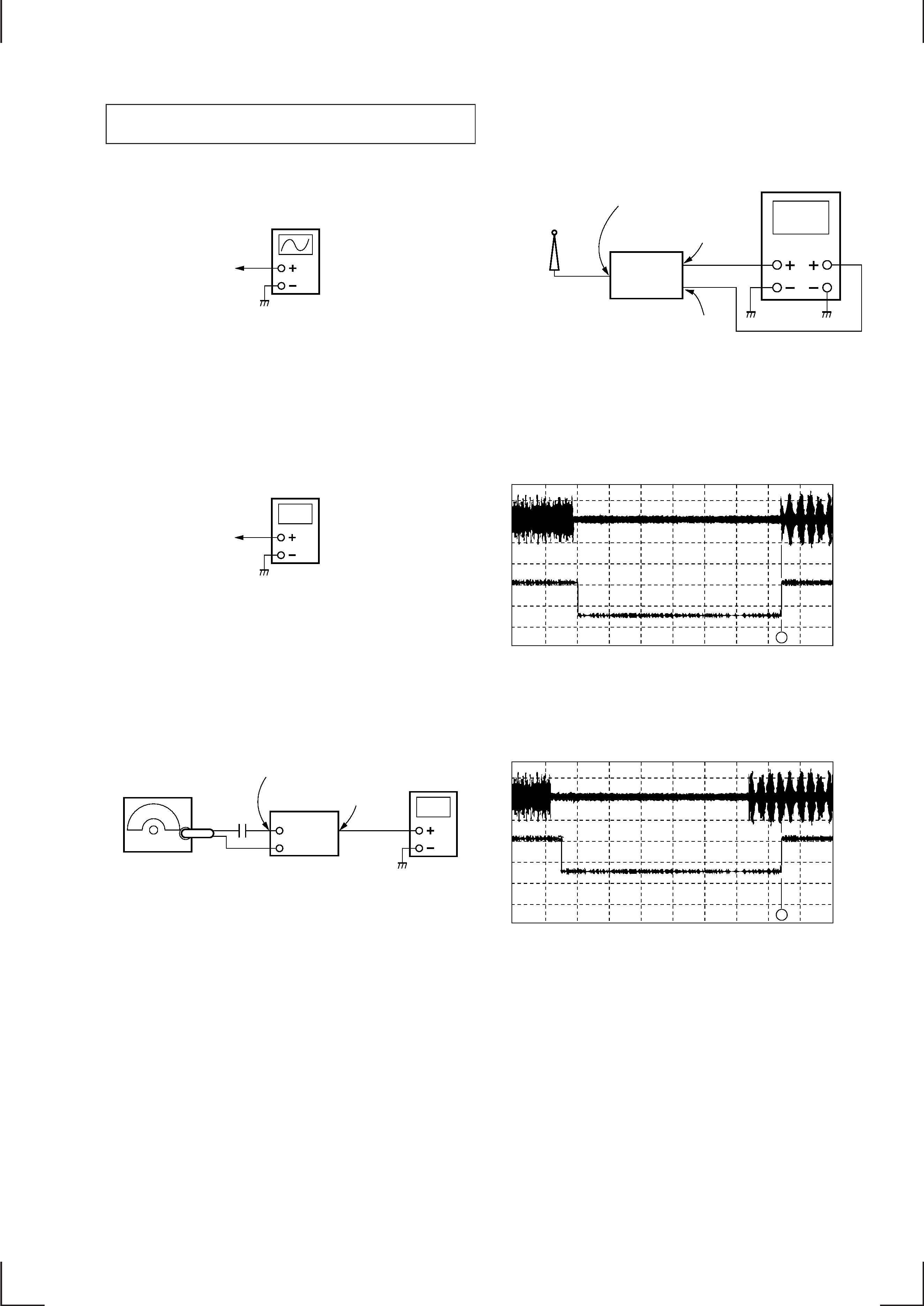
Local OSC Adjustment
Setting:
SECTION 3
ELECTRICAL ADJUSTMENTS
Procedure:
1. Adjust T102 so as to maximize the peak of waveform at 35.84
MHz.
Adjustment Location: See page 6.
IF2 Output Gain Adjustment
Setting:
oscilloscope
main board
TP LO
digital
voltmeter
main board
TP LEL
Procedure:
1. Adjust RV101 so that the reading on digital voltmeter is 2.25 V.
Adjustment Location: See page 6.
AGC Adjustment
Setting:
ANT +B switch : OFF
Procedure:
1. Set the carrier frequency of RF SSG to 225.648 MHz.
2. Receive the channel 12B (225.648 MHz).
3. Adjust RV102 so that the reading on digital voltmeter is 3.1
±
0.5 V.
4. Set the carrier frequency of RF SSG to 1471.792 MHz.
5. Receive the channel L12 (1471.792 MHz).
6. Adjust RV103 so that the reading on digital voltmeter is 3.2
±
0.5 V.
Adjustment Location: See page 6.
digital
voltmeter
main board
TP AGC
ANTENNA jack
0.01
µF
RF SSG
set
output level : 90 dBm (32 mV)
Non-modulation
Frame Sync Adjustment
Setting:
ANT +B switch : ON
Procedure:
1. Receive the DAB signal.
2. Adjust RV104 so that the rising edge of waveform of TP FSYNC
is positioned A.
(1) In case of Band
(from channel 5A to 13F)
(2) In case of L Band (from channel L1 to L23)
CH-1
CH-2
oscilloscope
main board
TP IF2
main board
TP FSYNC
ANTENNA jack
ANTENNA
set
TP
IF2
TP
FSYNC
A
1.68000 ms
680.00 us
200 us / div
320.00 us
realtime
1
500 mV/
2
2.00 V /
1.12500 V
5.00000 V
Adjustment Location: See page 6.
TP
IF2
TP
FSYNC
A
370.00 us
120.00 us
50.0 us / div
130.00 us
realtime
1
500 mV/
2
2.00 V /
125.000 mV
3.00000 V