1
MICROFILM
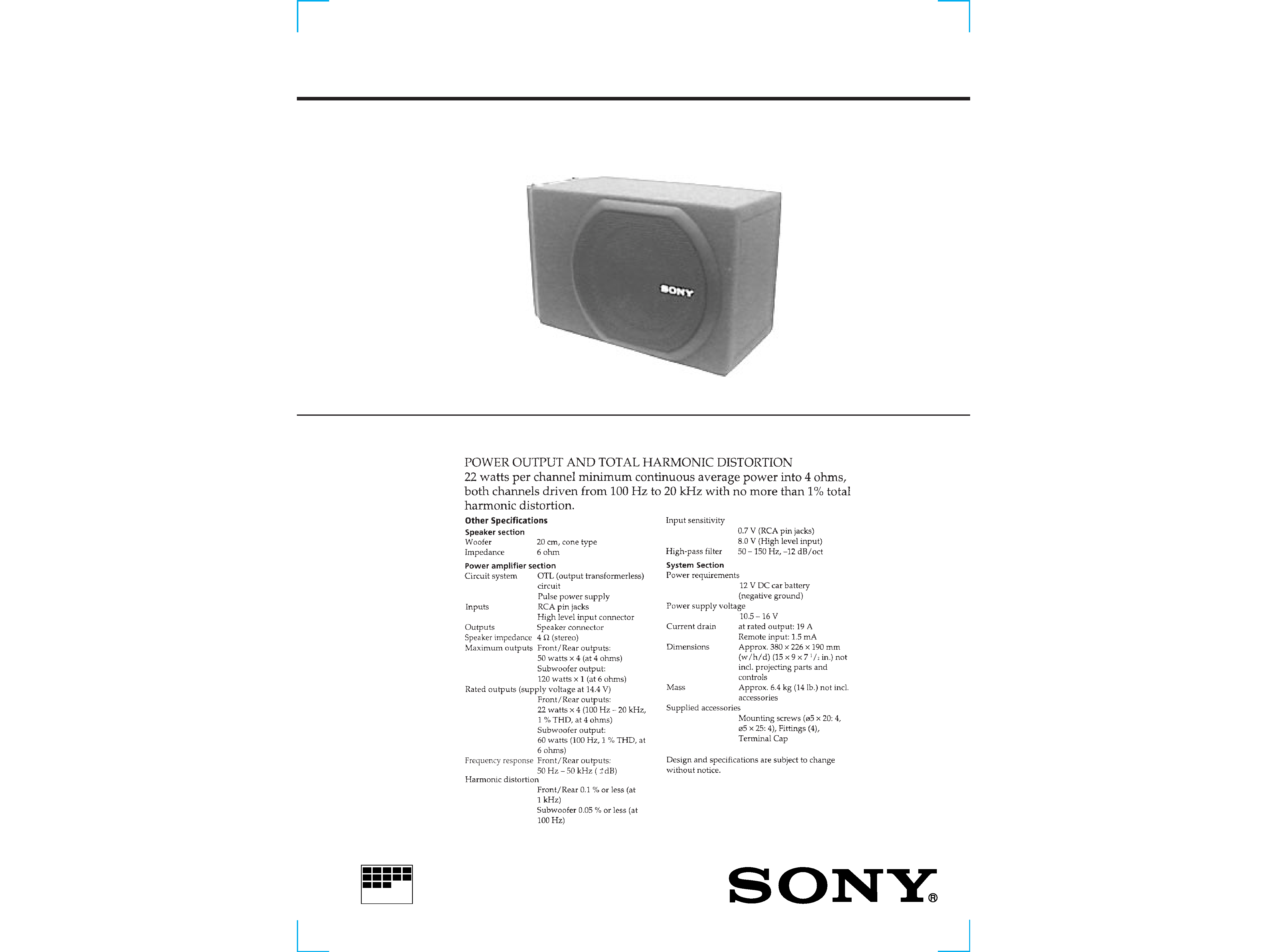
XS-AW850
SERVICE MANUAL
5 CHANNEL ACTIVE SUBWOOFER
US Model
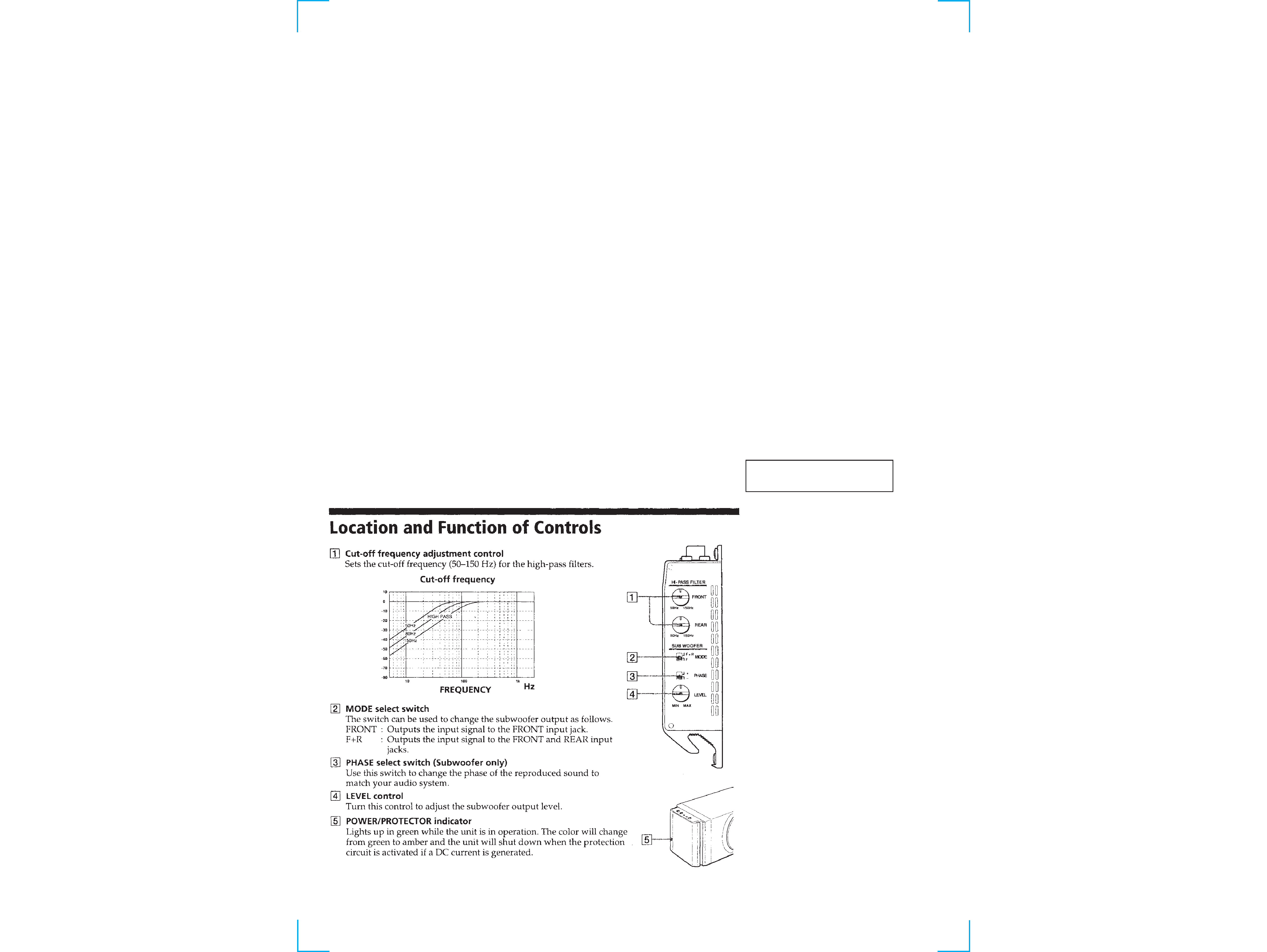
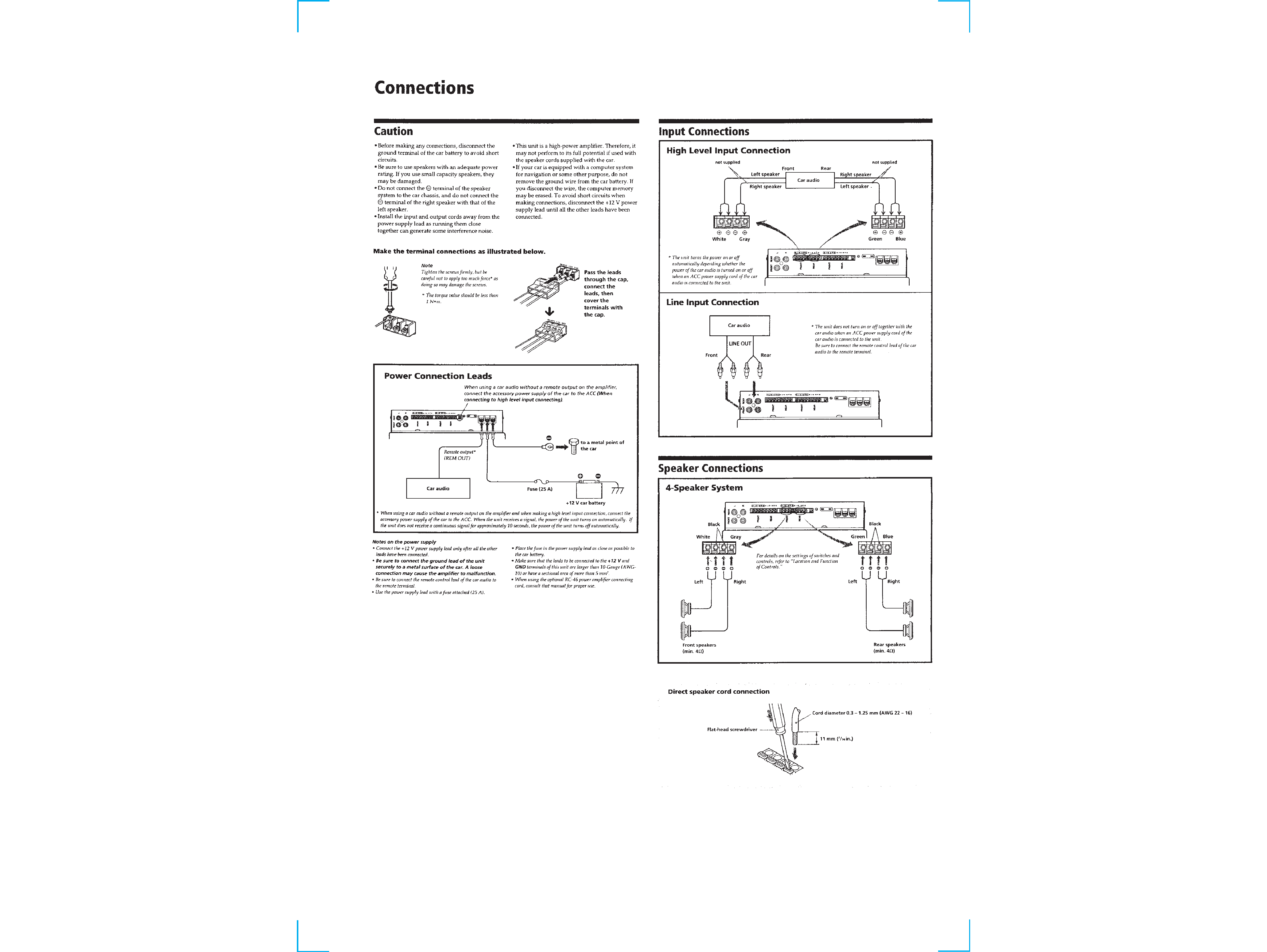
SPECIFICATIONS
2
Specifications ............................................................................. 1
1. GENERAL ....................................................................... 2
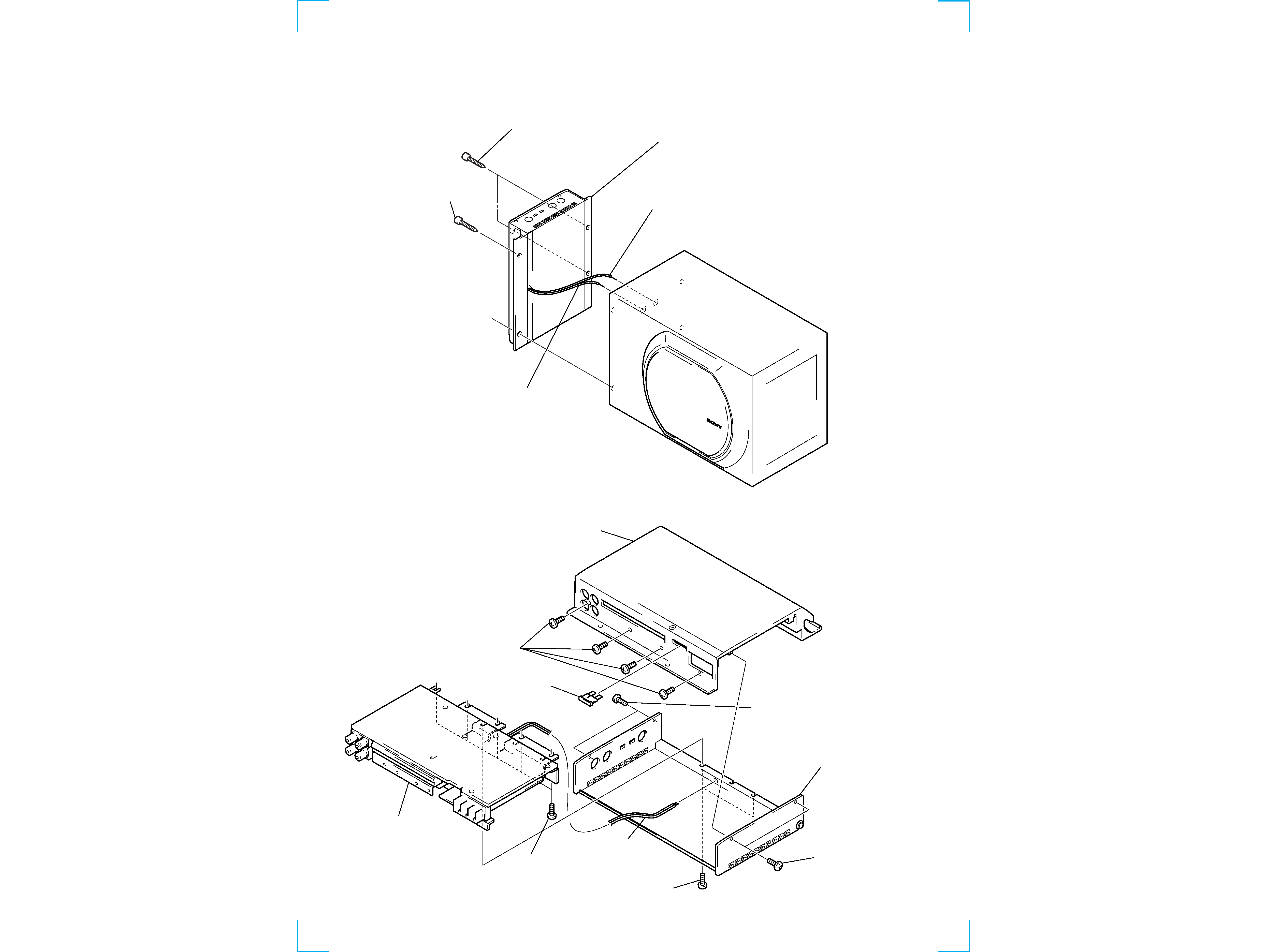
2. DISASSEMBLY
2-1. Amplifier Assembly ...................................................... 4
2-2. Main Board ................................................................... 4
2-3. DC Fan Motor ............................................................... 5
3. DIAGRAMS
3-1. IC Block Diagrams ....................................................... 6
3-2. Printed Wiring Board .................................................... 7
3-3. Schematic Diagram ....................................................... 9
4. EXPLODED VIEW ...................................................... 11
5. ELECTRICAL PARTS LIST .................................... 13
TABLE OF CONTENTS
SECTION 1
GENERAL
This section is extracted from
instruction manual.
3
4
SECTION 2
DISASSEMBLY
Note: Follow the disassembly procedure in the numerical order given.
2-1. AMPLIFIER ASSEMBLY
2-2. MAIN BOARD
1 Two tapping screws
(4x30)
2 Two tapping screws
(4x30)
3 Wire (White)
5 Amplifier assembly
4 Wire (Red)
1 Fuse (F901)
(Brade type)
5 Heat sink (MAIN)
8 Main board
9 Pull out a Wire.
0 Panel
2 Two screws
(BTP 3x8)
3 Two screws
(BTP 3x8)
4 Four screws
(BTP 3x8)
6 Three screws
(BTP 3x10)
7 Five screws
(BTP 3x10)
XS-AW850
5
6
SECTION 3
DIAGRAMS
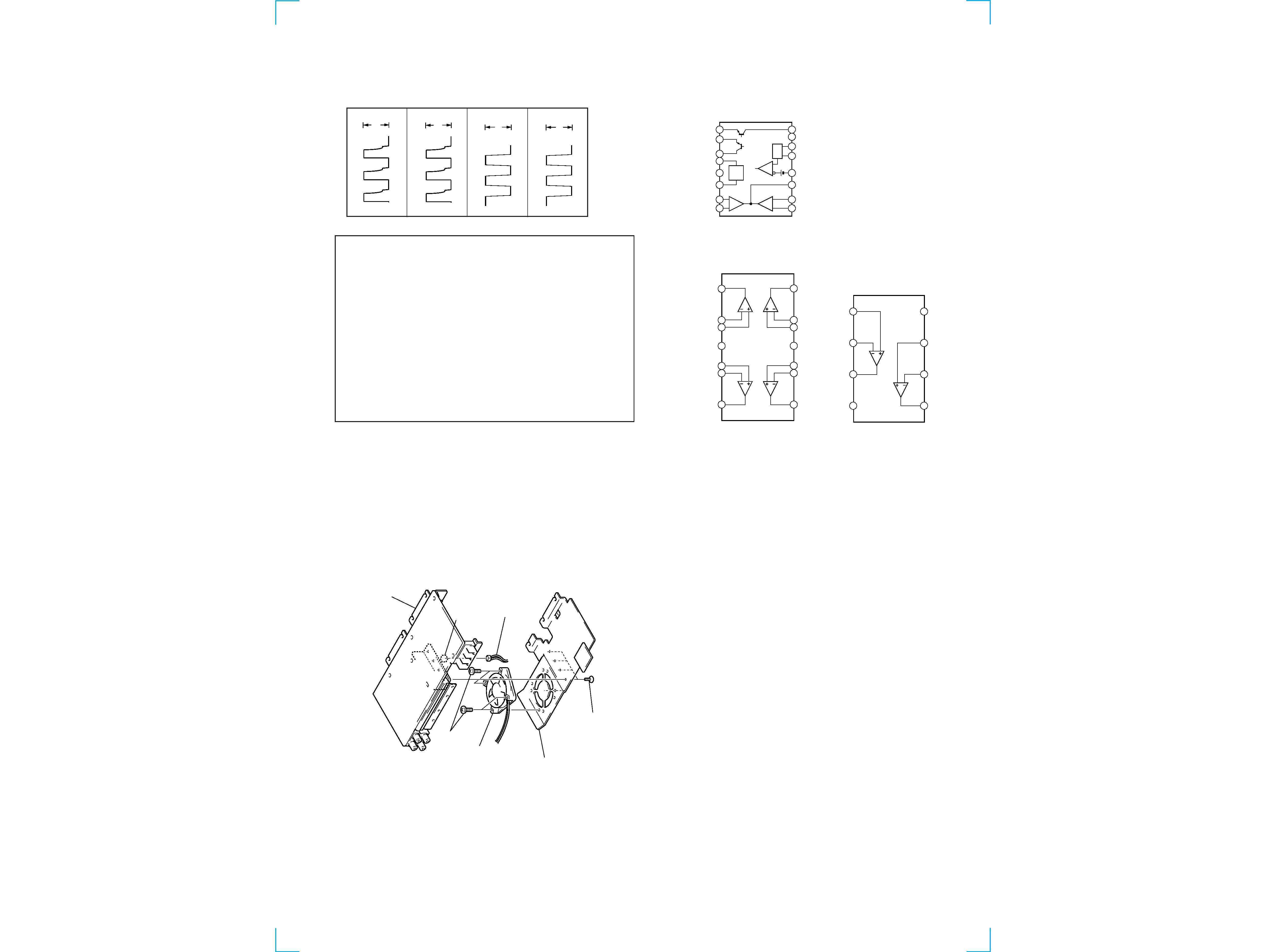
3-1. IC BLOCK DIAGRAMS
2-3. DC FAN MOTOR
IC101
µPC4570G2
IC602 LM2904M
IC901
µPC494GS
4
1
2
3
5
6
7 8
9
10
16 15
14
13
12 11
ERROR
0.1V
REG.
REF.
OSC
ERROR
Main baord
1 Four screws
(K 3x10)
4 Two screws
(BTP 3x14)
2 Connector (CN502)
3 Heat sink sub (A)
5 DC fan motor
(M901)
CN502
8
9
10
7
6
5
12
13
14
11
4
3
2
1
B-
B+
5
6
7
8
4
3
2
1
B-
B+
BO
VC
C
A+
GND
A-
AO
· WAVEFORMS
1
2
3
4
14Vp-p
27
µsec
29Vp-p
27
µsec
29Vp-p
27
µsec
60Vp-p
27
µsec
THIS NOTE IS COMMON FOR PRINTED WIRING
BOARDS AND SCHEMATIC DIAGRAMS.
(In addition to this, the necessary note is printed
in each block.)
For schematic diagrams.
Note:
· All capacitors are in µF unless otherwise noted. pF: µµF
50 WV or less are not indicated except for electrolytics
and tantalums.
· All resistors are in
and 1/4 W or less unless otherwise
specified.
·
¢
: internal component.
· C : panel designation.
· U : B+ Line.
· Power voltage is dc 14.4V and fed with regulated dc power
supply from ACC and BATT cords.
· Voltage and waveforms are dc with respect to ground
under no-signal conditions.
no mark : POWER ON
: Impossible to measure
· Voltages are taken with a VOM (Input impedance 10 M
).
Voltage variations may be noted due to normal production
tolerances.
· Waveforms are taken with a oscilloscope.
Voltage variations may be noted due to normal production
tolerances.
· Circled numbers refer to waveforms.
· Signal path.
F
: AUDIO
For printed wiring boards.
Note:
· X : parts extracted from the component side.
·
¢
: internal component.