1
MICROFILM
SERVICE MANUAL
US Model
Canadian Model
AEP Model
UK Model
E Model
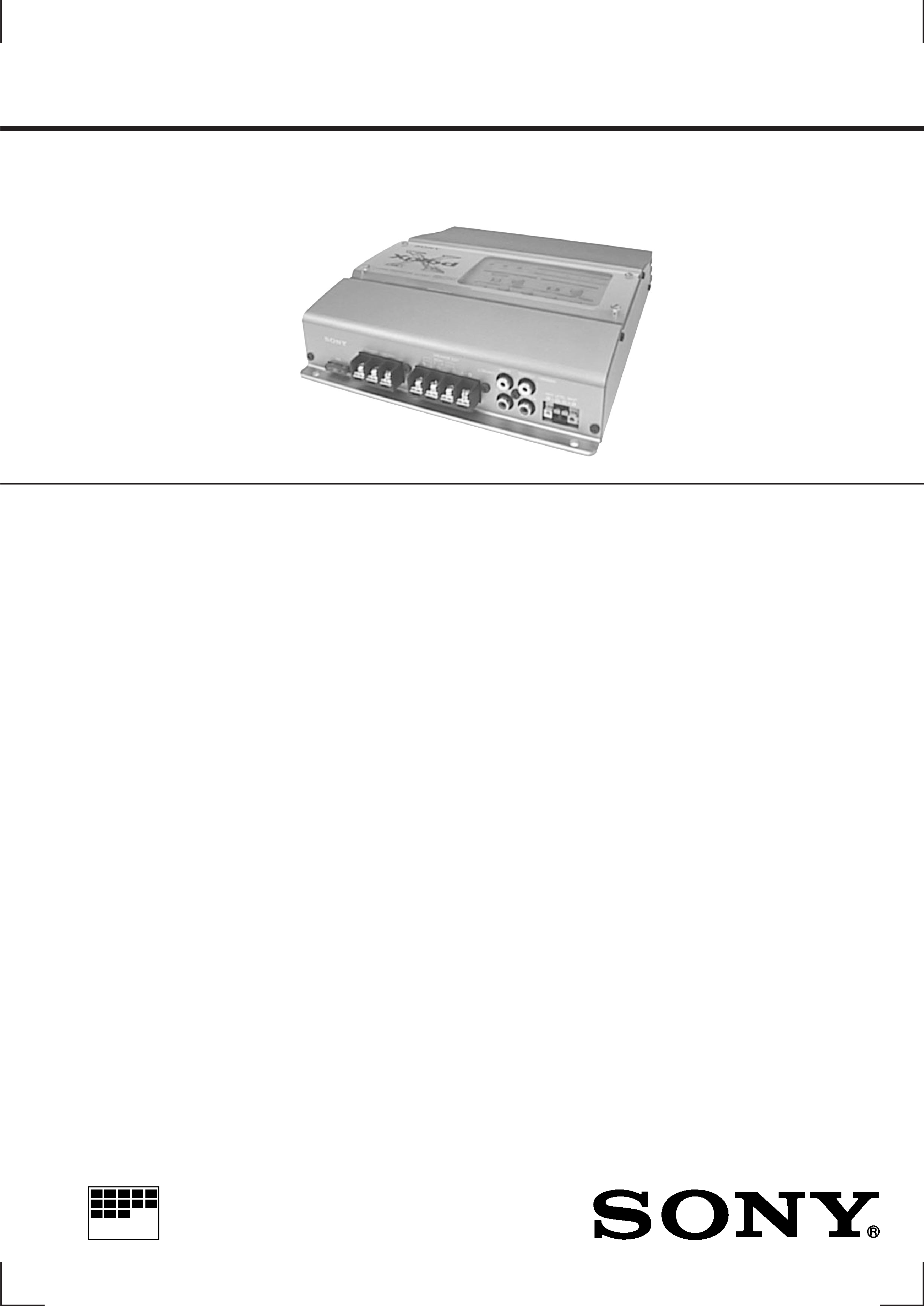
XM-752EQX
STEREO POWER AMPLIFIER
Other Specifications
Circuit system
OTL (output transformerless)
circuit
Pulse power supply
Inputs
RCA pin jacks
High level input connector
Outputs
Speaker terminals
Through out pin jacks
Speaker impedance
2 8
(stereo)
4 8
(when used as a bridging
amplifier)
Maximum outputs
150 watts
× 2 (at 4 )
400 watts (monaural, at 4
)
Rated outputs (supply voltage at 14.4 V)
75 watts per channel (20 Hz
20 kHz, 0.04% THD, at 4
)
100 watts per channel (20 Hz
20 kHz, 0.1% THD, at 2
)
200 watts (monaural) (20 Hz
20 kHz, 0.1% THD, at 4
)
Frequency response
5 Hz 100 kHz (
dB)
Harmonic distortion
0.005% or less
(at 1 kHz, 4
)
Input level adjustment range
0.2 4.0 V (RCA pin jacks)
0.4 8.0 V (High level input)
High-pass filter
50 200 Hz, 12 dB/oct
Low-pass filter
50 200 Hz, 12 dB/oct
Equalizer
50 Hz, 200 Hz, 800 Hz, 3.2 kHz,
12.8 kHz
±12 dB
Power requirements
12 V DC car battery
(negative ground)
Power supply voltage
10.5 16 V
Current drain
At rated output: 20 A
Remote input: 1.5 mA
Dimensions
Approx. 260
× 55 × 220 mm
(10 1/4
× 2 1/4 × 8 3/4 in.)
(l/h/p) not incl. projecting parts
and controls
Mass
Approx. 2.2 kg (4 lb. 14 oz.)
not incl. accessories
Supplied accessories
Mounting screws (4),
Terminal cap (1)
Design and specifications are subject to change without
notice.
SPECIFICATIONS
AUDIO POWER SPECIFICATIONS (US, Canadian model)
POWER OUTPUT AND TOTAL HARMONIC DISTORTION
75 watts per channel minimum continuous average power into
4 ohms, both channels driven from 20 Hz to 20 kHz with no more
than 0.04% total harmonic distortion per Car Audio Ad Hoc
Committee standards.
+0
3

2
TABLE OF CONTENTS
1. GENERAL
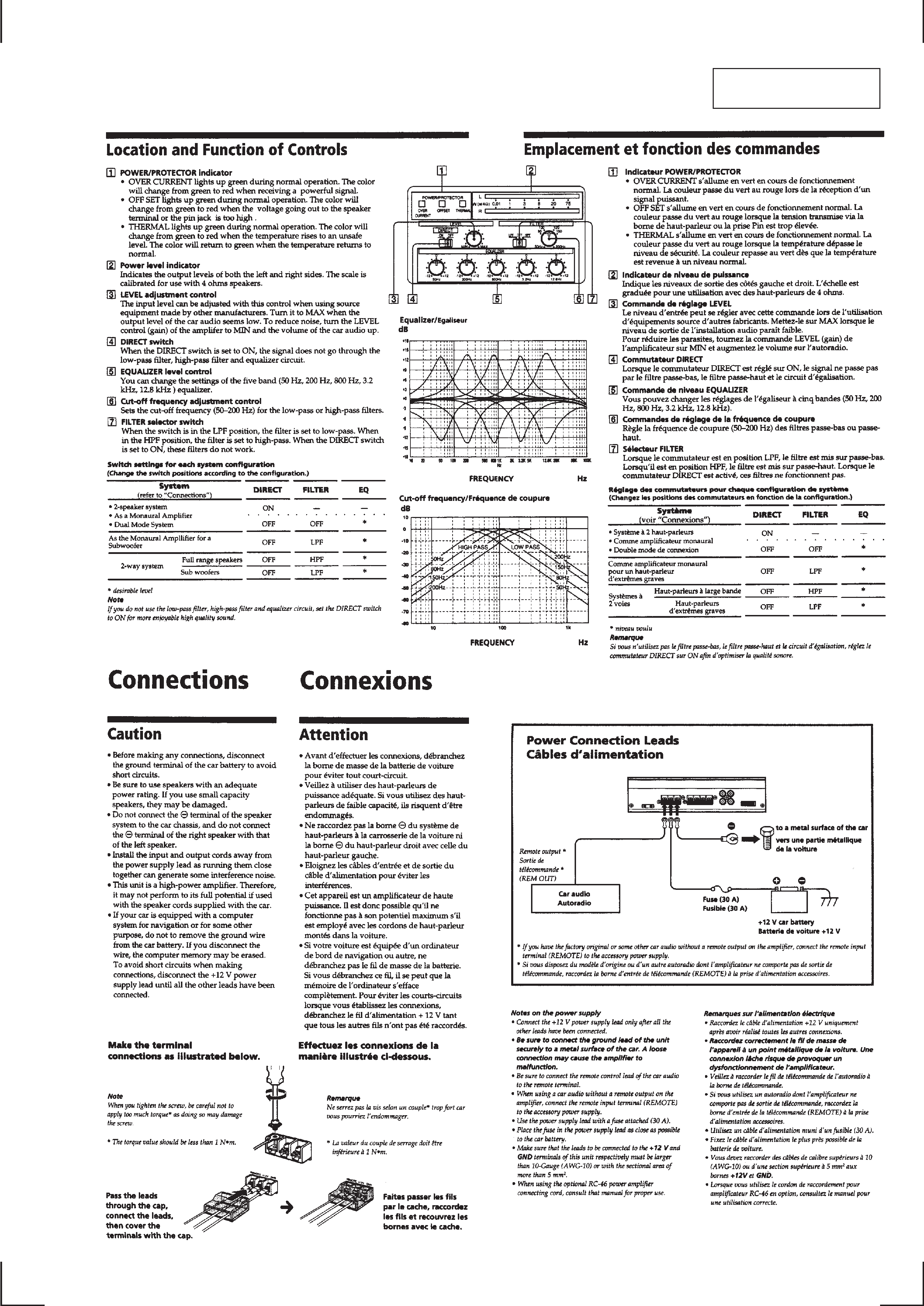
Location and Function of Controls .......................................... 3
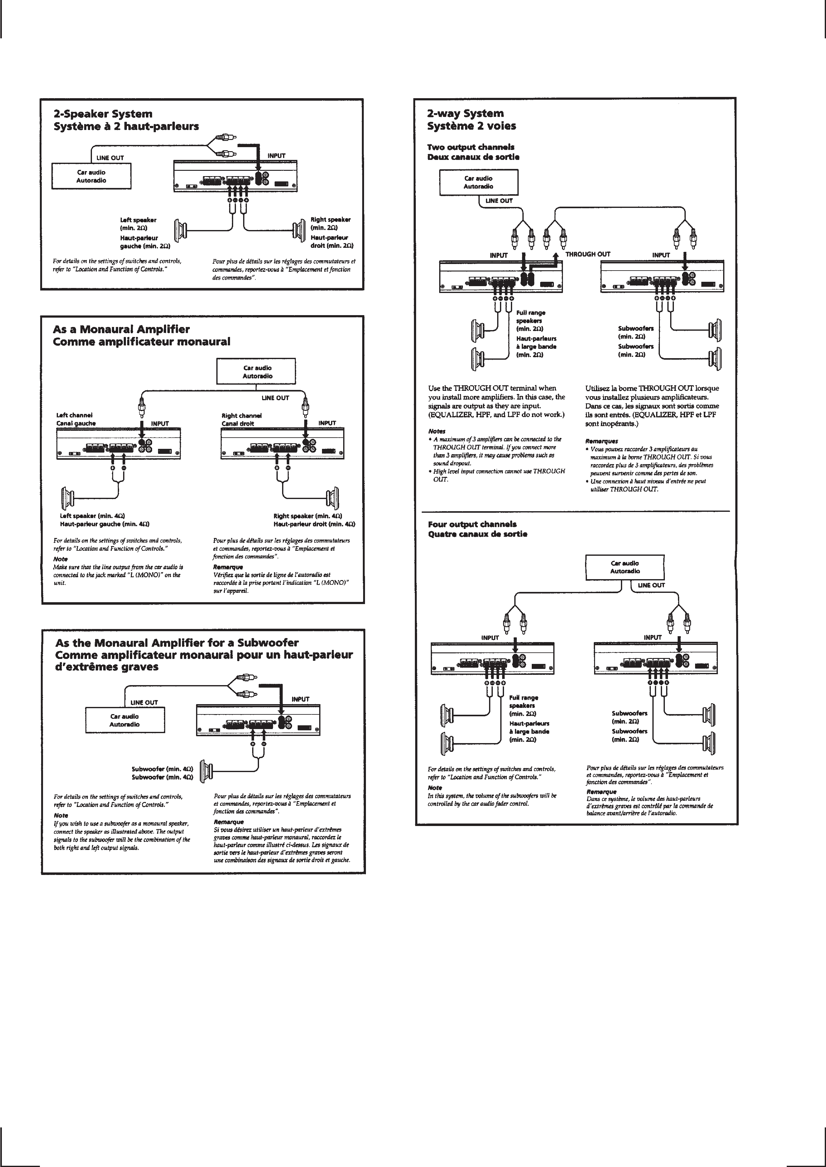
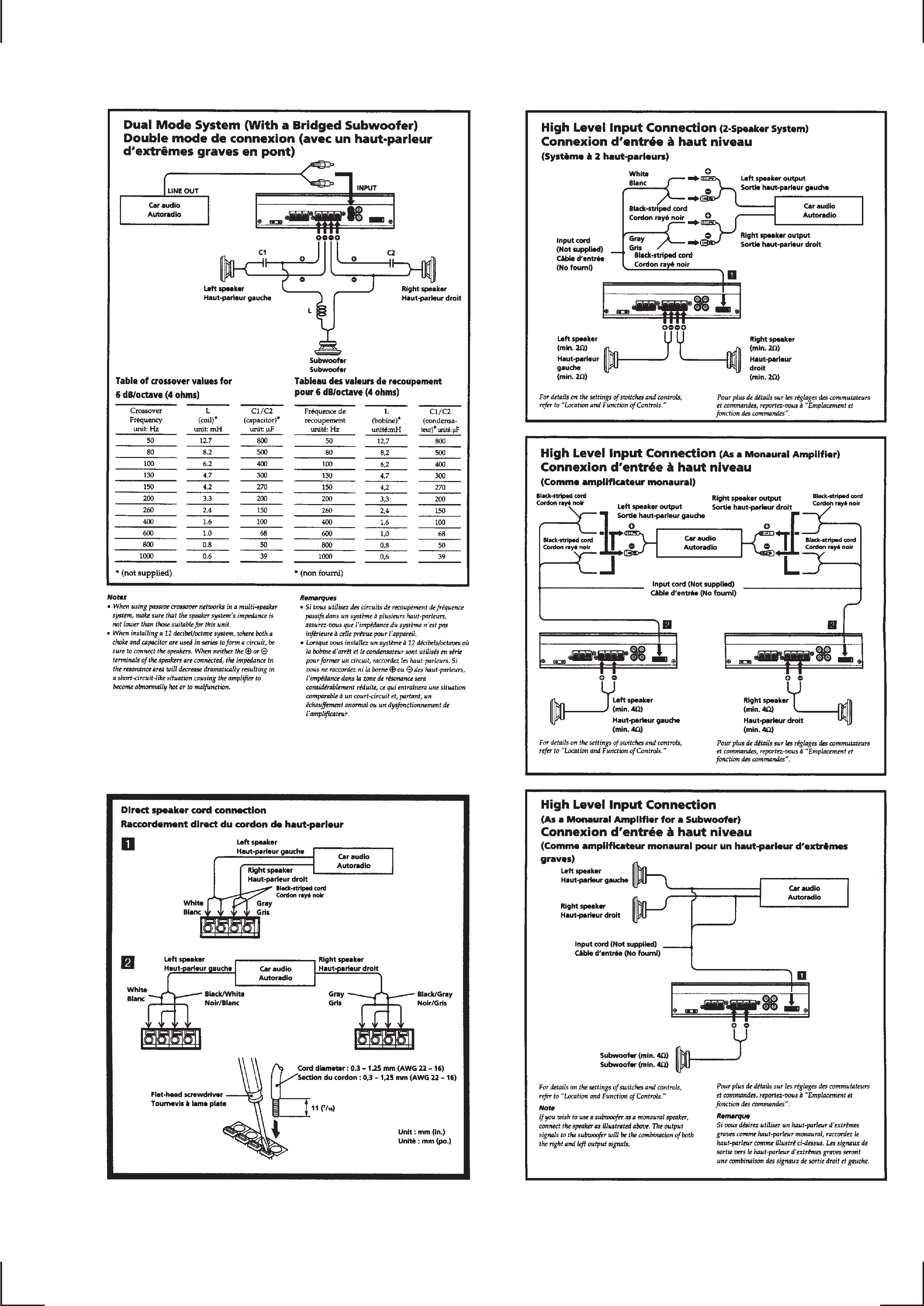
Connections ............................................................................. 3
2. DISASSEMBLY
2-1. Bottom Plate ........................................................................ 6
2-2. Panel (A) ............................................................................. 6
2-3. Panel (B) .............................................................................. 7
2-4. AMP Board ......................................................................... 7
2-5. Control Panel Block ............................................................ 8
3. DIAGRAMS
3-1. Block Diagram .................................................................... 9
3-2. Printed Wiring Board AMP Section .............................. 11
3-3. Schematic Diagram AMP Section ................................ 13
3-4. Schematic Diagram PRE Section .................................. 15
3-5. Printed Wiring Board PRE Section ............................... 15
3-6. Schematic Diagram EQ Section .................................... 17
3-7. Printed Wiring Board EQ Section ................................. 17
3-8. Printed Wiring Board IND Section ............................... 19
3-9. Schematic Diagram IND Section .................................. 20
3-10. Printed Wiring Board LED Section ............................... 21
3-11. Schematic Diagram LED Section ................................. 22
4. EXPLODED VIEWS
4-1. Heat Sink Section .............................................................. 24
4-2. Control Panel Section ........................................................ 25
5. ELECTRICAL PARTS LIST ........................................ 26
Notes on Chip Component Replacement
· Never reuse a disconnected chip component.
· Notice that the minus side of a tantalum capacitor may be dam-
aged by heat.
3
SECTION 1
GENERAL
This section is extracted
from instruction manual.
4
5