1
SERVICE MANUAL
SPECIFICATIONS
Power requirements
12 V DC car battery (negative
ground, 10.5 V 16 V)
Current drain
1 A
Frequency response
5 Hz 20 kHz
Signal-to-noise ratio
105 dB (Optical input)
Harmonic distortion
0.003 % (Optical input)
Separation
95 dB at 1 kHz
Input/output terminals
BUS input (1)
BUS output (1)
Line input (RCA jack) (2)
Line output (RCA jack) (4)
Optical digital input (2)
Dimensions
Approx. 249
× 45 × 183 mm
(9 7/8
× 1 13/16 × 7 1/4 in.) (w/h/d)
Mass
Approx. 2 kg (4 lb. 7 oz.)
Design and specifications are subject to change without
notice.
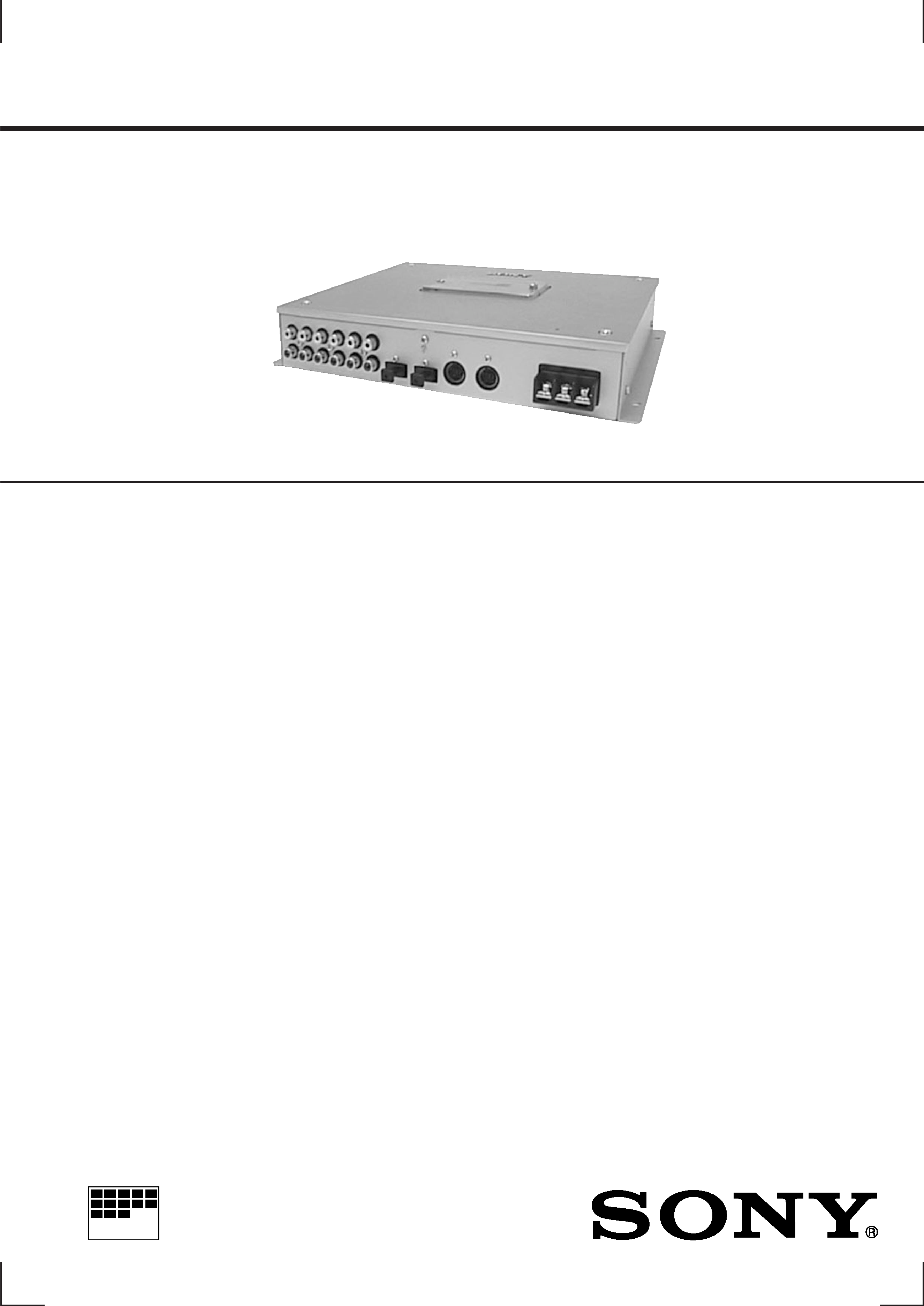
XDP-4000X
US Model
Canadian Model
AEP Model
UK Model
E Model
DIGITAL EQUALIZER PREAMPLIFIER
MICROFILM
Notes on Chip Component Replacement
· Never reuse a disconnected chip component.
· Notice that the minus side of a tantalum capacitor may be dam-
aged by heat.
2
SECTION 1
SERVICE NOTE
TABLE OF CONTENTS
1. SERVICE NOTE ................................................................. 2
2. GENERAL
Operation ................................................................................. 4
Connection ............................................................................... 5
3. DISASSEMBLY
3-1.
Case (Upper) ....................................................................... 7
3-2.
Main Board ......................................................................... 7
4. DIAGRAMS
4-1.
IC Pin Descriptions ............................................................ 8
4-2.
Block Diagram Input section ...................................... 15
4-3.
Block Diagram DSP section ....................................... 17
4-4.
Block Diagram Output section ................................... 19
4-5.
Printed Wiring Board Main Section ........................... 21
4-6.
Schematic Diagram Main Section (1/4) ..................... 25
4-7.
Schematic Diagram Main Section (2/4) ..................... 27
4-8.
Schematic Diagram Main Section (3/4) ..................... 29
4-9.
Schematic Diagram Main Section (4/4) ..................... 31
4-10. Schematic Diagram DAC, Intelligence,
Indicator Section ............................................................ 33
4-11. Printed Wiring Board DAC Section ........................... 35
4-12. Printed Wiring Boards Intelligence,
Indicator Section ............................................................ 37
5. EXPLODED VIEW ........................................................... 43
6. ELECTRICAL PARTS LIST ......................................... 44
+
BATT,ACC
GND
master unit
regulated DC
power supply
(14.4V)
+
B+
GND
regulated DC
power supply
(14.4V)
BUS CONTROL IN
BUS CONTROL IN
(MASTER)
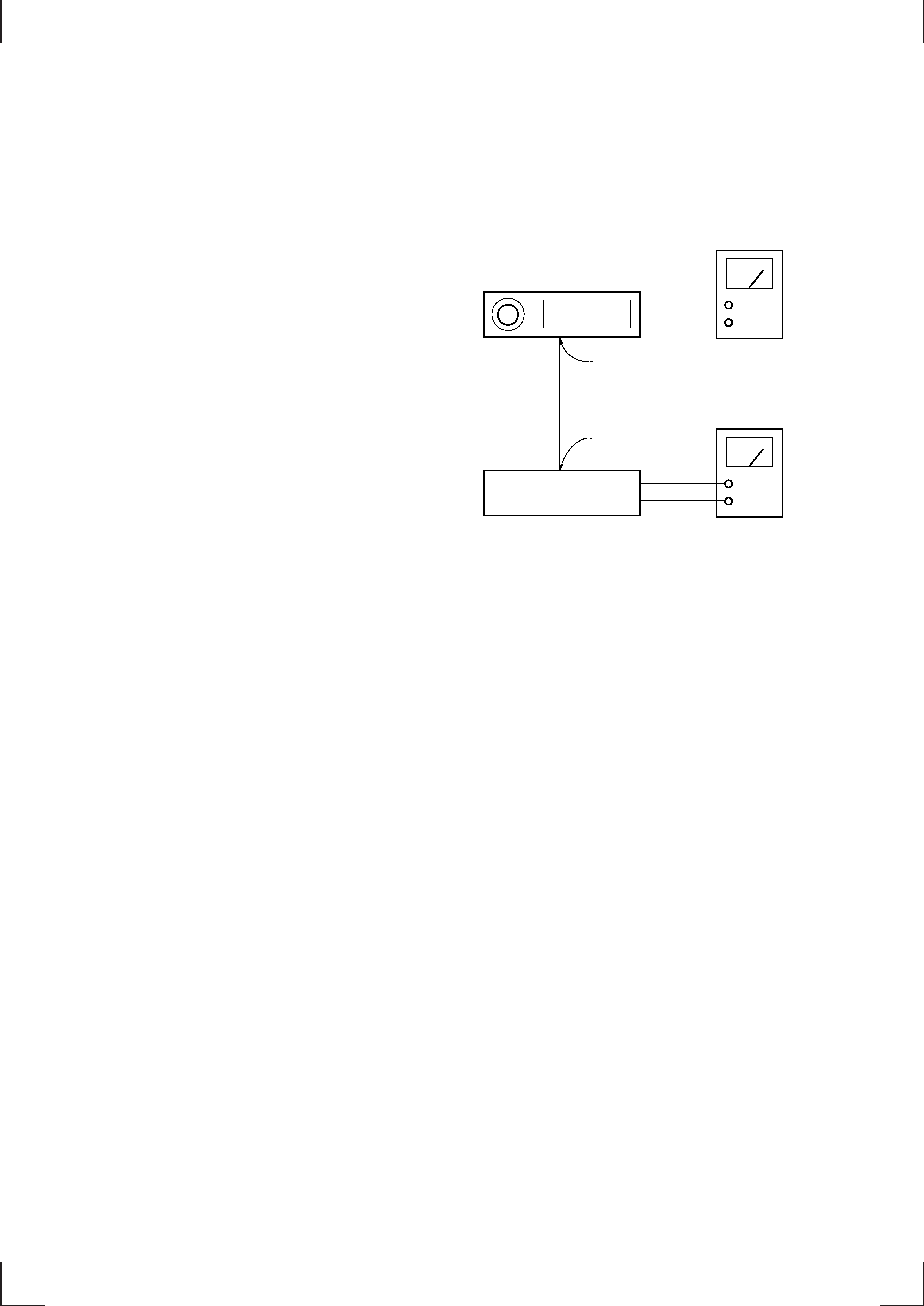
XDP-4000X
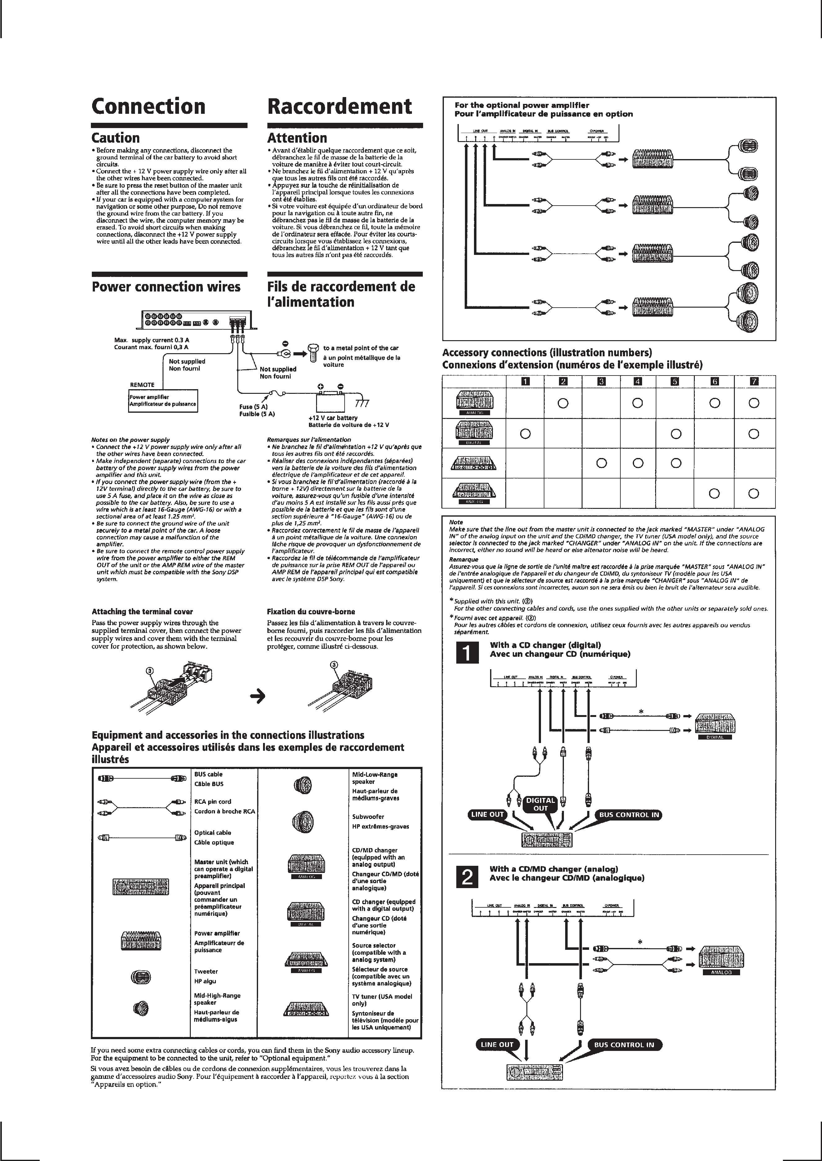
METHOD OF OPERATING THE XDP-4000X
This set cannot be operated alone.
To operated this, it should be connected with a master unit such as
CDX-C880 or XR-C9100 as shown below.
3
1
2
3
4
5
6
7
8
9
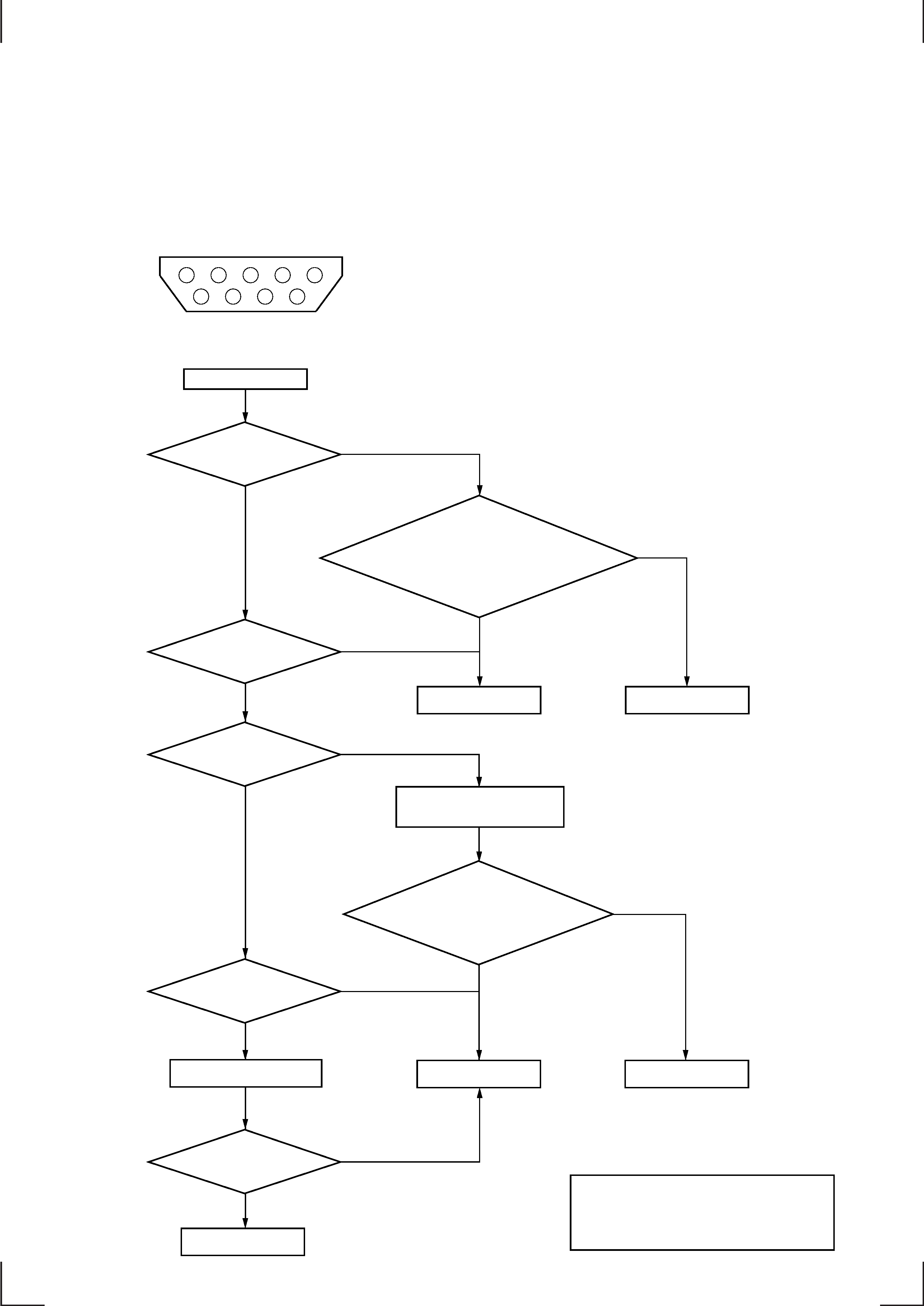
METHOD OF DETERMINING ACCEPTANCE OR REJECTION OF
INTELLIGENCE BOARD (A-3317-137-A) OF XDP-4000X
· No parts in the intelligence board can be repaired.
If the intelligence board is defective, the whole board
should be replaced.
Pin numbers of 9-pin D-SUB connector (CN707)
(viewed from the top of the set)
Note that the voltage given in the following
descriptions is relative to the ground power pin.
Intelligence board check
Is voltage at pin
!º of IC707 +5V?
Is voltage at pin
3 of CN707
between 8 and 9V ?
Is the resistance between pin
1 of CN703
and ground hundreds of 100 kilohms or more
Pull cable out of CN703 on main board.
Is voltage at pin
2 of the CN703 +5V?
Intelligence board at fault
Intelligence board at fault
Intelligence board is normal
Main board at fault
Set ACC-OFF and pull cable out of
CN703 on main board
Main board at fault
Yes
Yes
Yes
Yes
Is voltage at pin
9 of IC707 +5V?
Is voltage at pin
2 of CN707 0V?
Is voltage at pin
9 of IC707 0V?
Add 8 to 9V to pin
2 of CN707
Yes
Yes
Yes
No
No
No
No
No
No
No
The fault of the main board may be caused by one of the
following:
1. Shorted CN703 (OPEN).
2. Shorted pins
!TM and !¢ of IC702 (OPEN).
3. Damaged port of IC702.
4
This section is extracted
from instruction manual.
SECTION 2
GENERAL
5