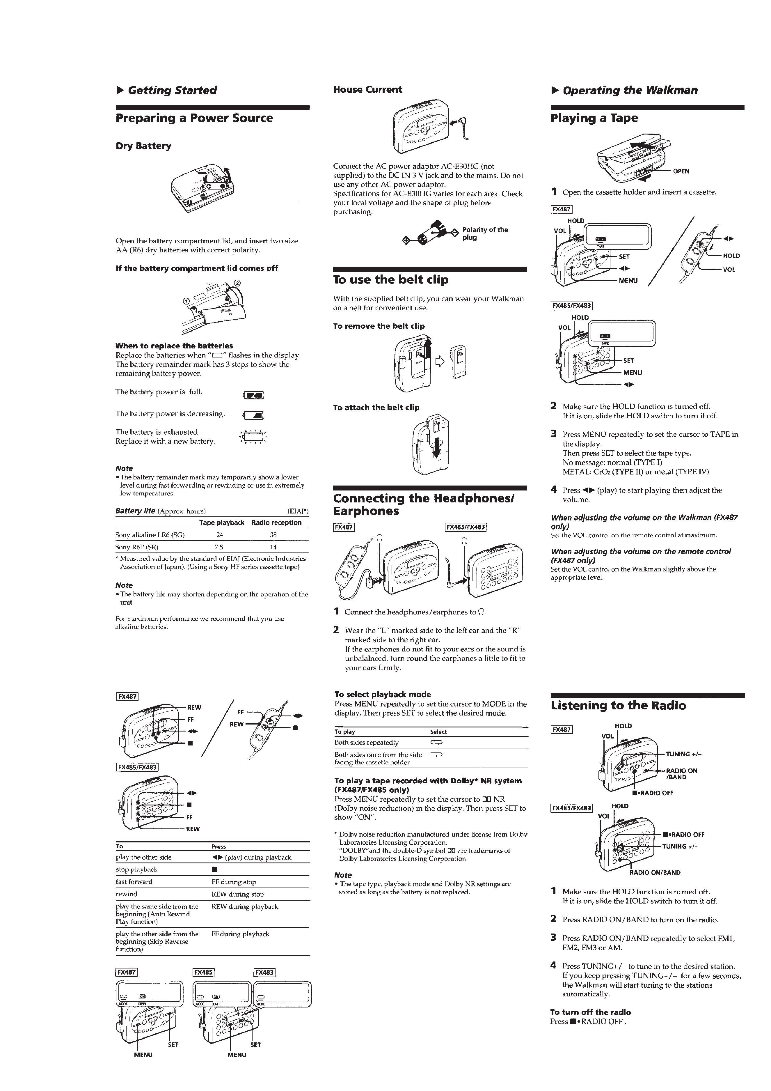
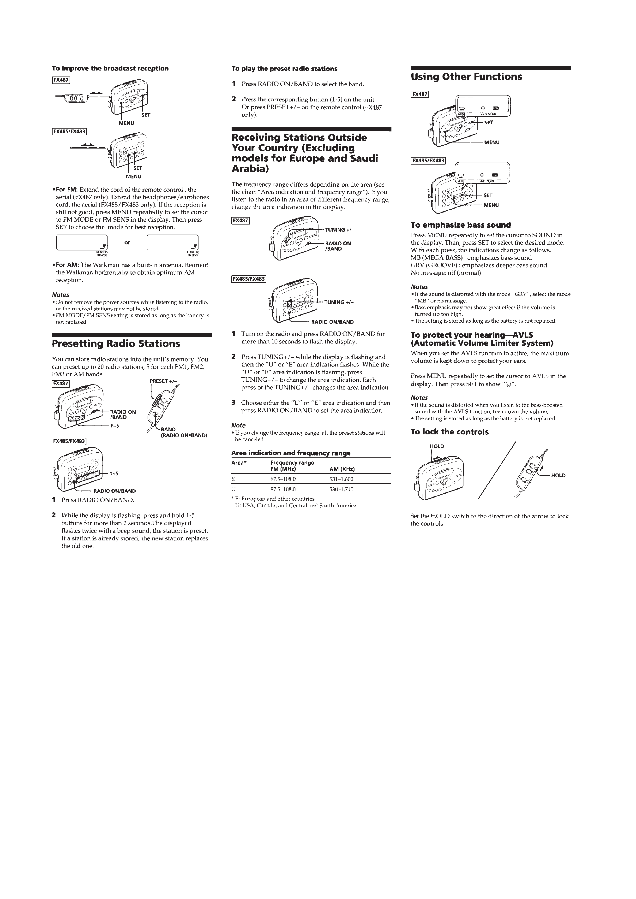
WM-FX483/FX485/FX487
US Model
WM-FX487
Canadian Model
WM-FX485/FX487
AEP Model
E Model
WM-FX483/FX485/FX487
SERVICE MANUAL
RADIO CASSETTE PLAYER
MICROFILM
Model Name Using Similar Mechanism
WM-EX402/EX404/EX405/EX406
Tape Transport Mechanism Type
MF-WMFX483-147
SPECIFICATIONS
Manufactured under license from Dolby
Laboratories Licensing Corporation.
"DOLBY" and the double-D symbol a are
trademarks of Dolby Laboratories Licensing
Corporation.
Design and specifications are subject to change without notice.
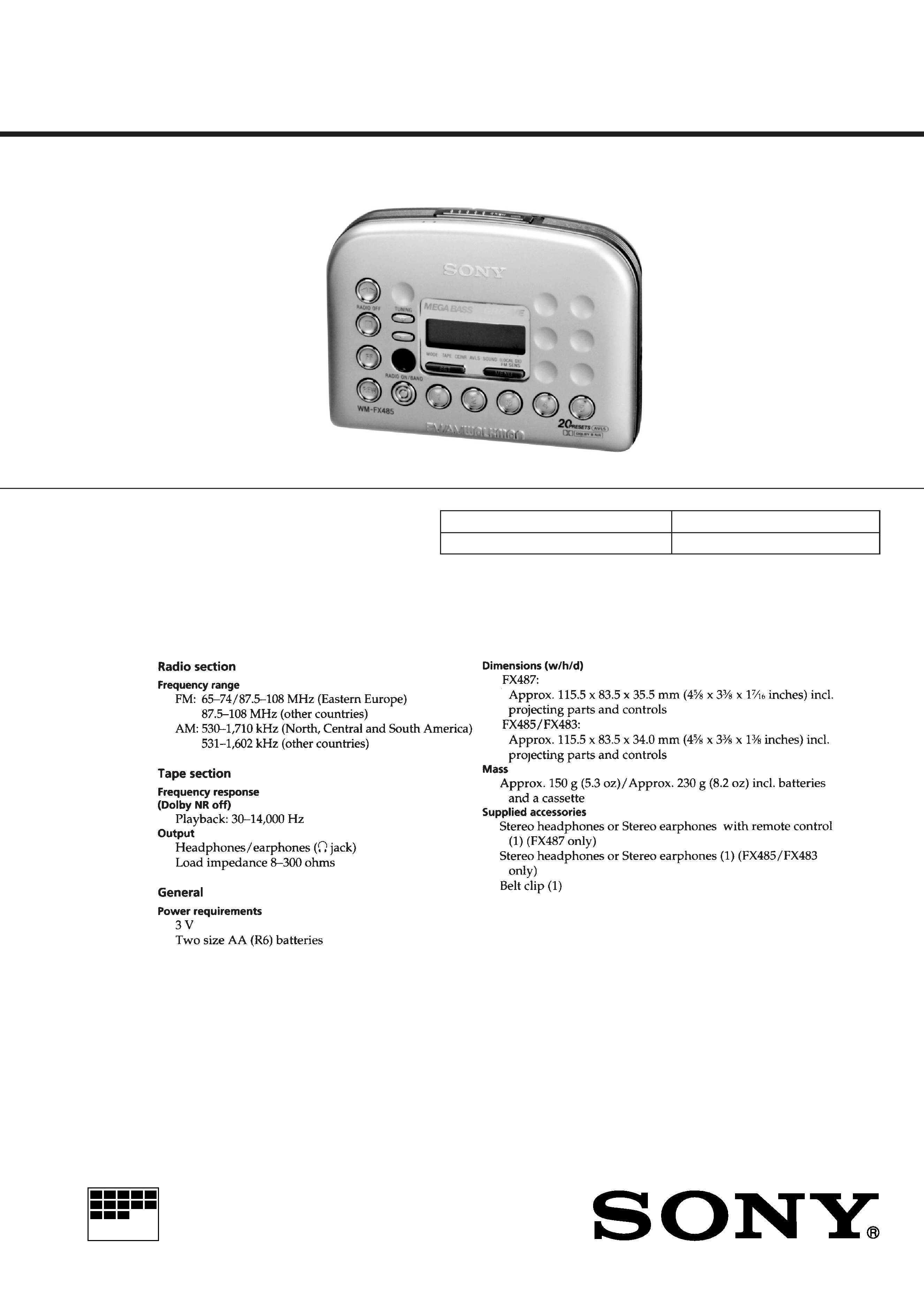
Photo : WM-FX485
Ver 1.0 1998.03

-- 2 --
TABLE OF CONTENTS
Flexible Circuit Board Repairing
·
Keep the temperature of the soldering iron aroud 270° C during
repairing.
·
Do not touch the soldering iron on the same conductor of the
circuit board (within 3 times).
·
Be careful not to apply force on the conductor when soldering
or unsoldering.
Notes on chip component replacement
·
Never reuse a disconnected chip component.
·
Notice that the minus side of a tantalum capacitor may be
damaged by heat.
1.
GENERAL ······································································ 3
2.
DISASSEMBLY
2-1.
Cabinet (Front) Assy ·························································· 5
2-2.
Main Board ········································································· 6
2-3.
Mechanism Deck ································································ 6
2-4.
Cassette Lid Sub Assy ························································ 7
2-5.
Display Board ····································································· 7
3.
MECHANICAL ADJUSTMENT······························· 8
4.
ELECTRICAL ADJUSTMENT ································ 8
5.
DIAGRAMS
IC Block Diagrams ··························································· 11
5-1.
Block Diagram ································································· 13
5-2.
Printed Wiring Board -Main Section- ······························ 15
5-3.
Schematic Diagram -Main Section- ································· 17
5-4.
Printed Wiring Board -Display Section-(FX483/FX485)·· 19
5-5.
Schematic Diagram -Display Section-(FX483/FX485) ···· 21
5-6.
Printed Wiring Board -Display Section-(FX487) ·············· 23
5-7.
Schematic Diagram -Display Section-(FX487) ················ 25
5-8.
IC Pin Function ································································ 27
6.
EXPLODED VIEWS
6-1.
Cassette Lid Section ························································· 29
6-2.
Cabinet Section································································· 31
6-3.
Mechanism Deck Section ················································· 32
7.
ELECTRICAL PARTS LIST ··································· 33
SECTION 1
GENERAL
-- 3 --
-- 4 --
-- 5 --
SECTION 2
DISASSEMBLY
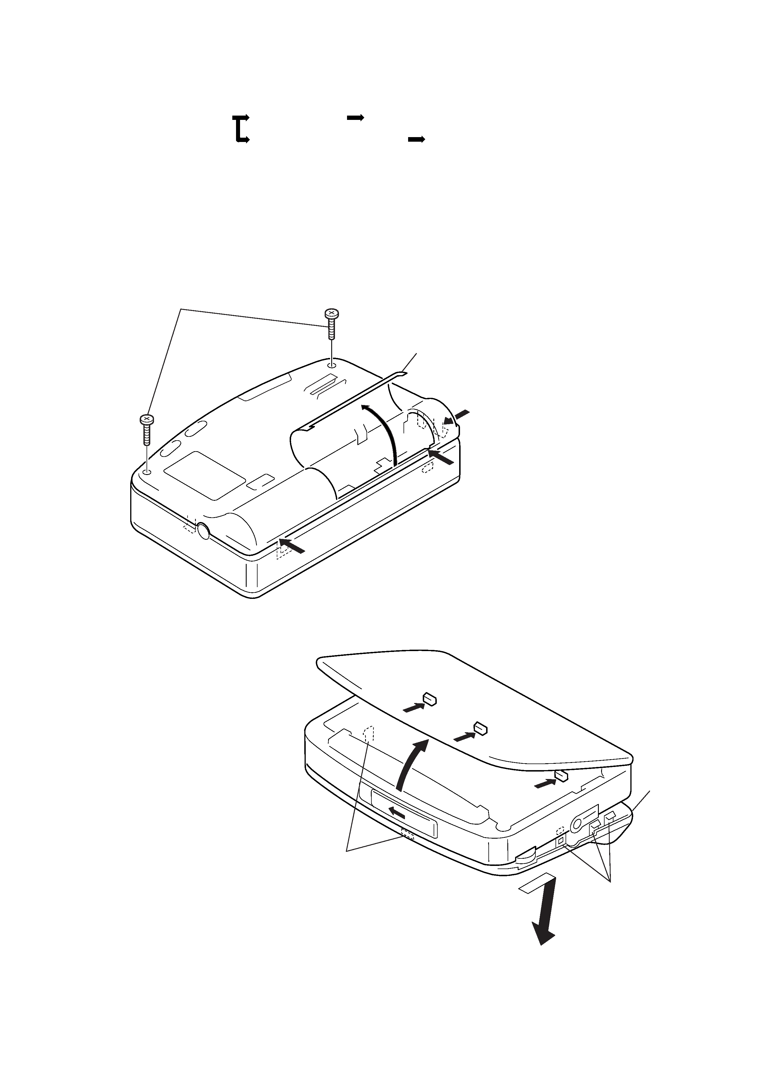
Note : Follow the disassembly procedure in the numerical order given.
2-1.
CABINET (REAR) ASSY
· This set can be disassembled in the order shown below.
2-1. CABINET (REAR) ASSY
2-2. MAIN BOARD
2-4. CASSETTE LID SUB ASSY
2-3. MECHANISM DECK
2-5. DISPLAY BOARD
1 Screw (B 1.7
× 12), tapping
2 Open the lid battery case.
3
3
3
Cabinet (rear) assy
Claws
Claws
6
5
5
5
4