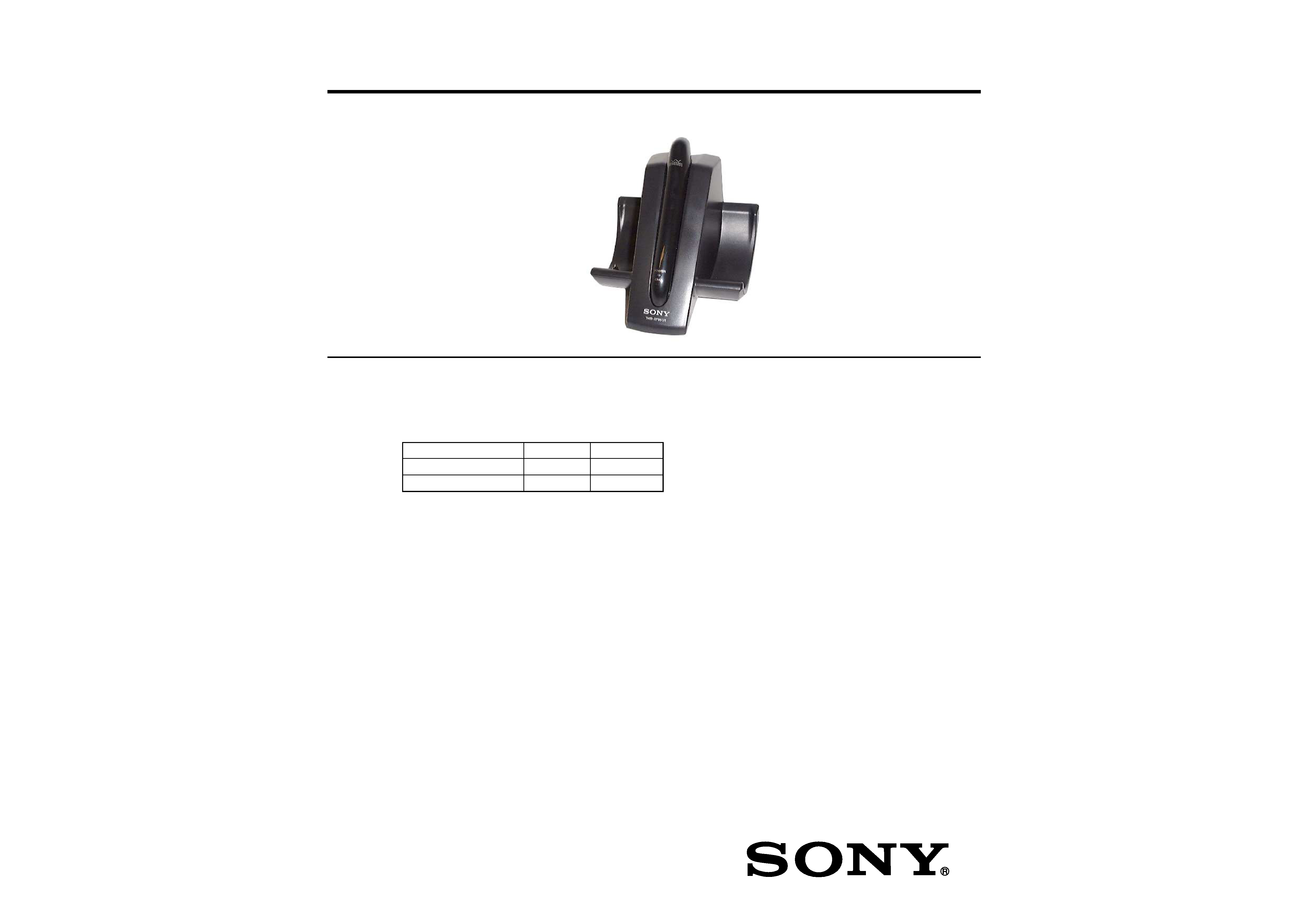
TMR-RF960R
US Model
Canadian Model
SERVICE MANUAL
TRANSMITTER
Sony Corporation
Personal Audio Company
Published by Sony Engineering Corporation
9-877-526-01
2004B02-1
© 2004.02
SPECIFICATIONS
Ver 1.0 2004. 02
TMR-RF960R is the component model block one in the MDR-RF960RK
or MDR-RF920RK.
MDR-RF920RK MDR-RF960RK
Wireless Stereo Headphones MDR-RF920R
MDR-RF960R
Transmitter
TMR-RF960R
TMR-RF960R
COMPONENT MODEL NAME FOR MDR-RF920RK/
MDR-RF960RK
General
Carrier frequency
913.5 914.5 MHz
Channel
Ch1, Ch2, Ch3
Modulation
FM stereo
Frequency response
MDR-RF920R : 20 20,000 Hz
MDR-RF960R : 10 22,000 Hz
Transmitter
Power source
DC 9 V: supplied AC power adaptor
Audio input
phono jacks/stereo mini jack
Dimensions
Approx. 133 x 124 x 136 mm
(5 1/4 x 5 x 5
3/
8 in.)
(w/h/d)
Mass
Approx. 195 g (7 oz.)
2
TMR-RF960R
SECTION 1
GENERAL
1. Check the area of your repair for unsoldered or poorly-sol
deredconnections. Check the entire board surface for solder
splashes and bridges.
2. Check the interboard wiring to ensure that no wires are
"pinched" or contact high-wattage resistors.
3. Look for unauthorized replacement parts, particularly
transistors, that were installed during a previous repair.
Point them out to the customer and recommend their
replacement.
4. Look for parts which, through functioning, show obvious signs
of deterioration. Point them out to the customer and
recommend their replacement.
SAFETY CHECK-OUT
5. Check the B+ voltage to see it is at the values specified.
6. Flexible Circuit Board Repairing
·
Keep the temperature of the soldering iron around 270
°C
during repairing.
·
Do not touch the soldering iron on the same conductor of
the circuit board (within 3 times).
·
Be careful not to apply force on the conductor when
soldering
TABLE OF CONTENTS
Specifications ............................................................................ 1
1.
GENERAL ................................................................... 2
2.
DISASSEMBLY
2-1. Upper Cabinet Assy ............................................... 3
2-2. TX-BASE Board .................................................... 3
3.
ELECTRICAL ADJUSTMENTS .......................... 4
4.
DIAGRAMS
4-1. Block Diagrams ...................................................... 5
4-2. Schematic Diagram TX-BASE Board ............. 6
4-3. Printed Wiring Board TX-BASE Board ........... 7
4-4. Schematic Diagram TX-VCO Board ............... 8
4-5. Printed Wiring Board TX-VCO Board ............ 8
5.
EXPLODEDVIEWS .................................................. 10
6.
ELECTRICAL PARTS LIST ............................... 11
This section is extracted
from instruction manual.
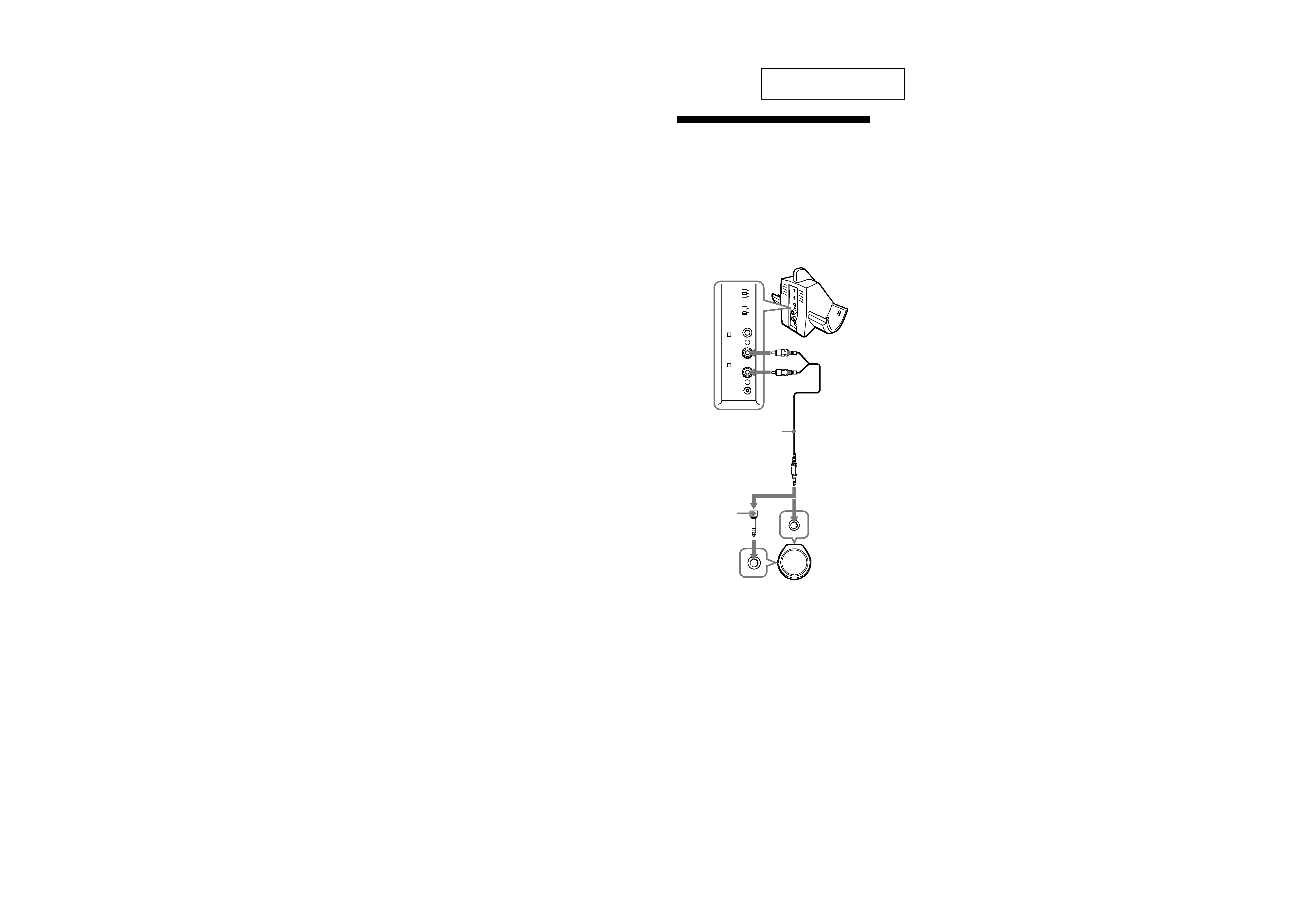
INPUT
A
INPUT
DC IN 9V
!
L
R
B
NOISE FILTER
ON
OFF
CHANNEL
1
2
3
Setting up the
transmitter
1 Connect the transmitter to audio/
video equipment.
Select one of the hookups below
depending on the jack type:
A
To connect to a headphones jack
Transmitter
WALKMAN*,
TV, VCR, etc.
to INPUT B
jacks
Unimatch plug
adaptor
(supplied)
to headphones
jack (stereo
phone jack)
Connecting cord
(supplied)
to headphones
jack (stereo
mini jack)
Left channel
(white)
Right channel
(red)
After correcting the original service problem, perform the following
safety checks before releasing the set to the customer.
3
TMR-RF960R
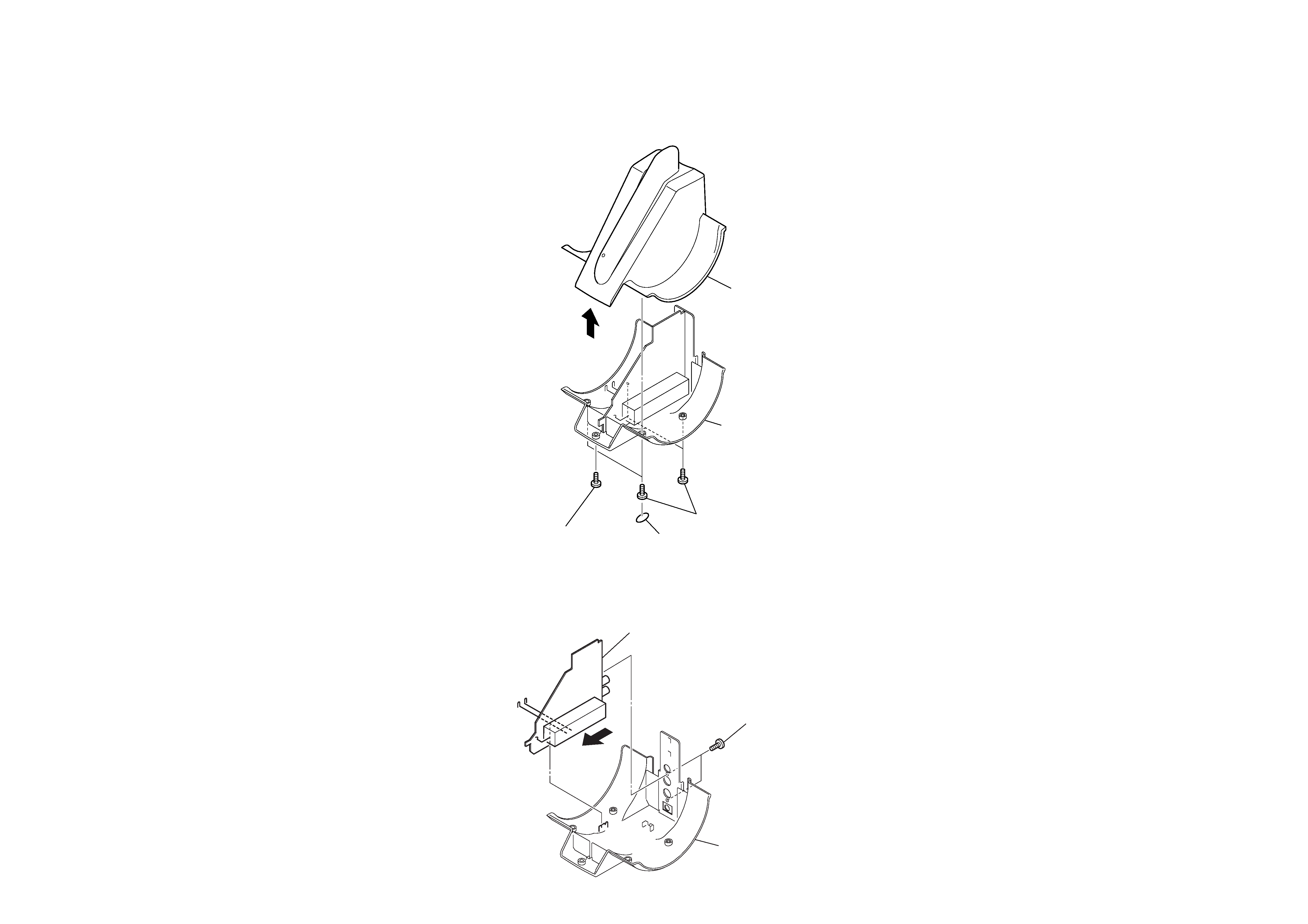
SECTION 2
DISASSEMBLY
2-2.
TX-BASE BOARD
· This set can be disassembled in the order shown below.
2-1. UPPER CABINET ASSY
1
protection sheet
5
upper cabinet assy
2
screw (DIA. 2)
3
four screws (DIA. 2)
4
cabinet (lower) assy
1
two screws (DIA. 2)
3
TX-BASE board
2
cabinet (lower) assy
4
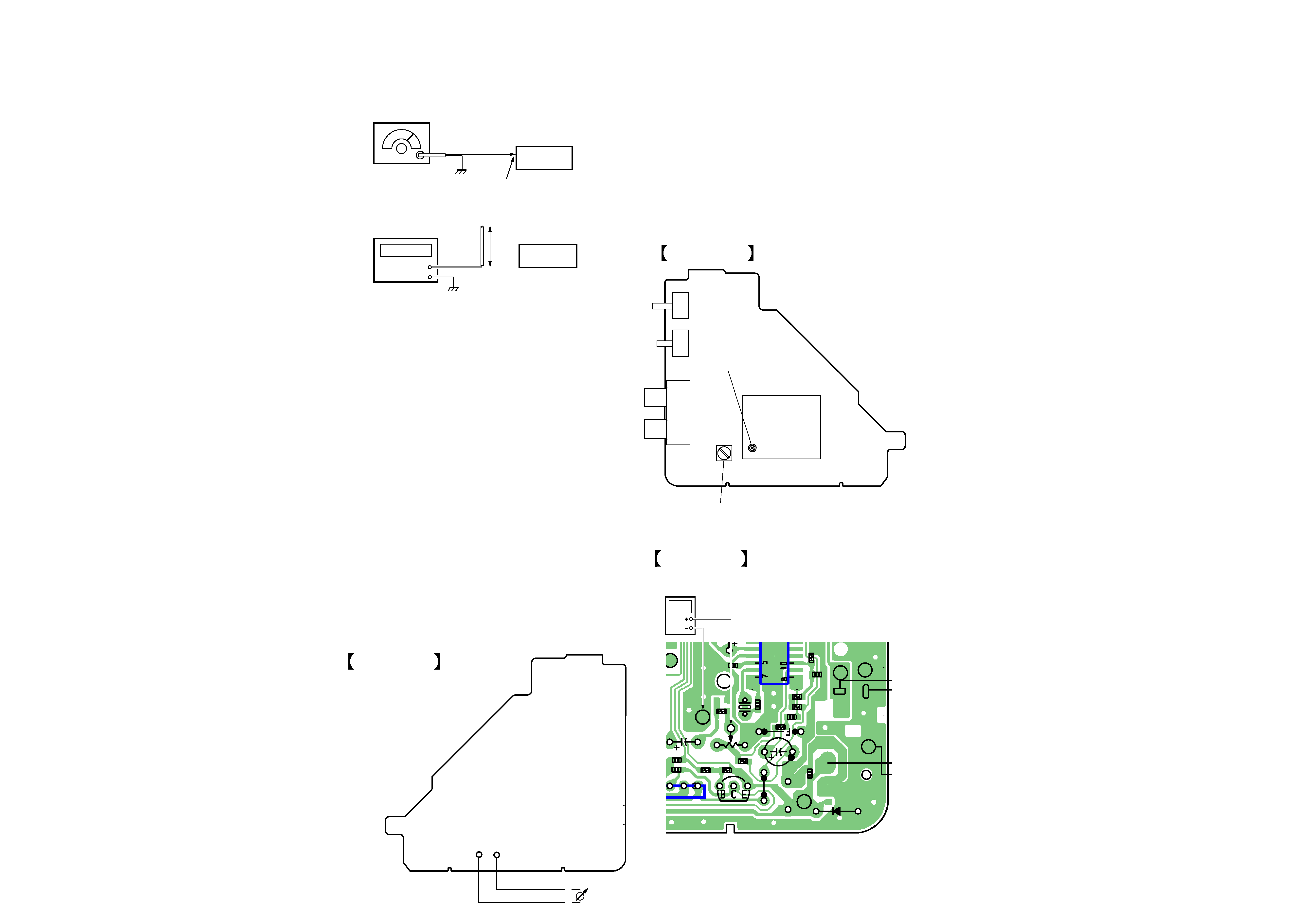
TMR-RF960R
SECTION 3
ELECTRICAL ADJUSTMENTS
Setting :
AF signal
generator
Telescopic
antenna
8 cm
L-CH (J402)
TMR-RF960R
set
TMR-RF960R
set
Frequency counter
Transmission Frequency Check
1.
Set the noise filter SW to OFF.
2.
Input a signal of 1 kHz 40 mVrms to only the L-CH (J402).
3. Connect a telescopic antenna to the frequency counter input
and extend the antenna to a length of approximately 8 cm.
4. Place TX-BASE board close to the frequency counter, then
measure the frequencies of CH1, CH2 and CH3 and make
sure the values are as follows:
CH1 : 913.5 MHz
± 200 kHz
CH2 : 914.0 MHz
± 200 kHz
CH3 : 914.5 MHz
± 200 kHz
When the frequency is not satisfied the specified value, set the
channel switch (S402) to CH2, then adjust the value of the frequency
counter to 914.0 MHz by CT501 in the TX-VCO BLOCK.
Standard value :913.9MHz to 914.1MHz
When completed with replacement, recheck the frequencies of CH1,
CH2 and CH3.
Charge Current Check
1. Connect the ammmeter 3 and # probes to TP8 and 9.
2. The green LED (on charging) turns on.
Make sure the reading on the current meter becomes to the
standard value.
Standard value: 45
±5mA
TP8 TP9
CURRENT METER
3
#
TX-BASE BOARD (Conductor side)
Pilot signal Modulation Check and Adjustment
1. Set the channel to CH2.
2. An electric wave is output for 5 or 10 minutes when OFF to
ON a power supply (LED (POWER) will ON).
3. Measure the center terminal of RV401 using an digital volt-
meter (AC range) and make sure the value is 2.65 to
2.75mVrms.
If the measured value is other than the specified value, adjust
to 2.65 to 2.75mVrms by turning the RV401 on the TX-BASE
board.
Connection points and Adjustment Location :
RV401
TX-VCO BLOCK
(R-CH)
(L-CH)
CHANNNEL
3CH-2CH-1CH
RV401: Modulation adjustment
CT501:Transmission
frequency adjustment
TX-BASE BOARD (Component side)
S402
S401
J402
8
3
2
1
R468
R466
C488
C455
C454
C457
R469
R460
R464
R402
C480
R405
R472
IC404
IC403
C408
D403
X401
C458
RV401
JW416
JW401
IC402
Q404
C450
1-861-437-
digtal voltmeter
(AC range)
TX-BASE BOARD (Conductor side)
TMR-RF960R
5
5
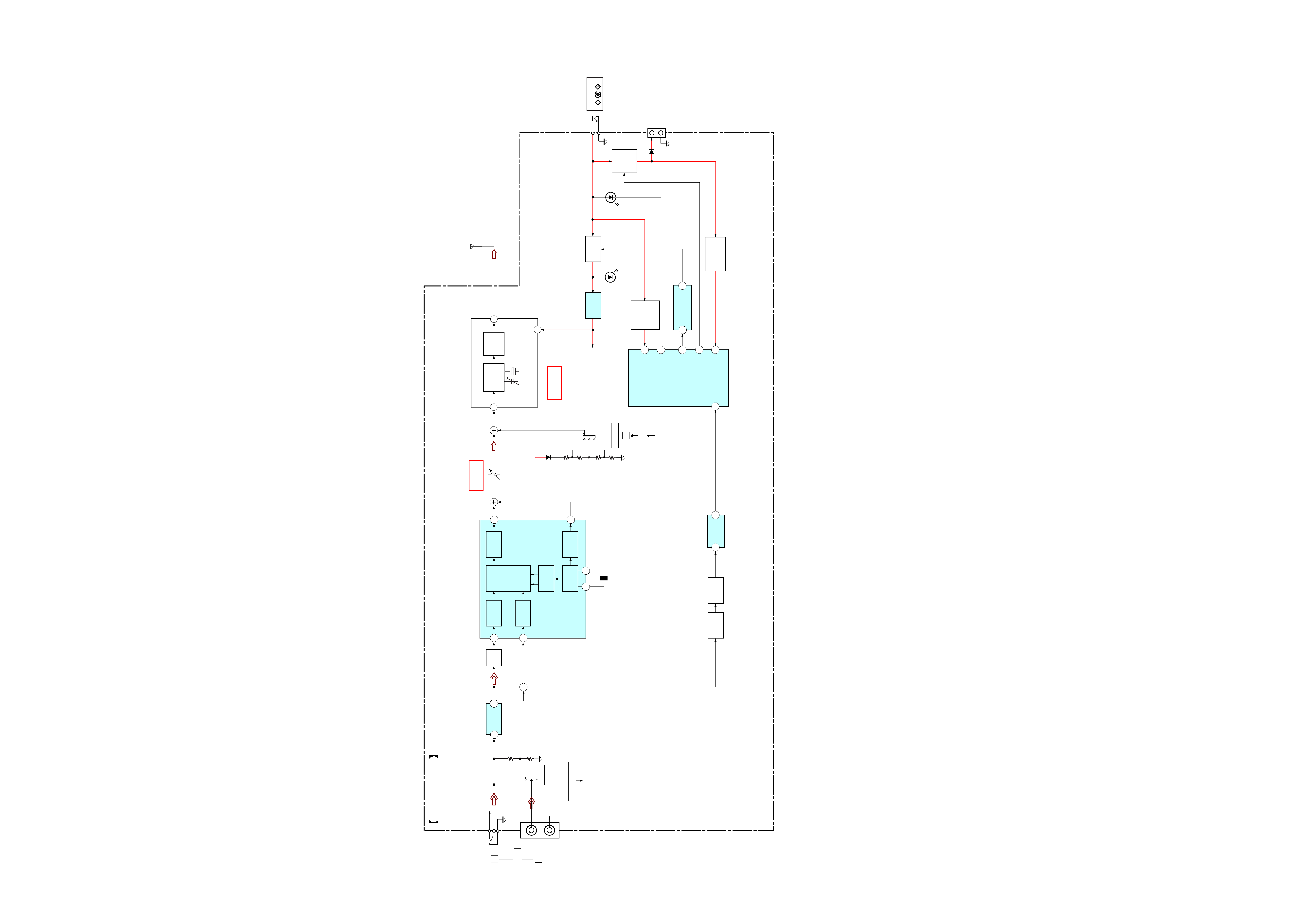
4-1. BLOCK DIAGRAM
J401
S401
NOISE FILTER
COMPARATOR
(POWER ON/OFF)
ALC
AMP
CH2
AMP
BUFFER
AMP
Q401
RECT
D404,405
INPUT
DET
DIVIDER
(19K)
BUFFER
OSC
AMP
TIME
DEVISION
MPX
J402
OFF
ON
L
R
R-CH
R-CH
R-CH
14
9
8
7
6
CH1
AMP
1
X401
38kHz
RV401
IC401
LPF
Q408
IC403
STEREO MPX
+5V
REG
SWITCH
Q404
IC402
ANT401
D401
D402
(POWER)
(CHARGE)
INPUT
B
A
TX-BASE BOARD
MOD
IN
ANT
5V
B+
5V
TX-VCO BLOCK
I
O
V
PILOT SIGNAL
MODULATION
REGULATOR
&
RIPPLE
FILTER
Q402
Q406,407
CHARGE
DET
S402
CHANNEL
1
2
B+
5V
3
BATTERY
CHARGE
TERMINAL
(TO MDR-RF920R/RF960R)
+
J403
DC IN 9V
CHARGE
CURRENT
LIMIT
Q405,410
1
13
R-CH
+
3
1
20
17
16
18
12
1
Q403
COMPENSATION
MODULATOR
Q501,502
RF AMP
Q503
X501
1080MHz
5
7
IC405(2/2)
IC405(1/2)
SYSTEM
CONTROL
IC404
D407
CT501
TRANSMISSION
FREQUENCY
CT501
· R-ch is omitted due to same as L-ch
· Signal path.
L
: AUDIO
F
: FM
SECTION 4
DIAGRAMS