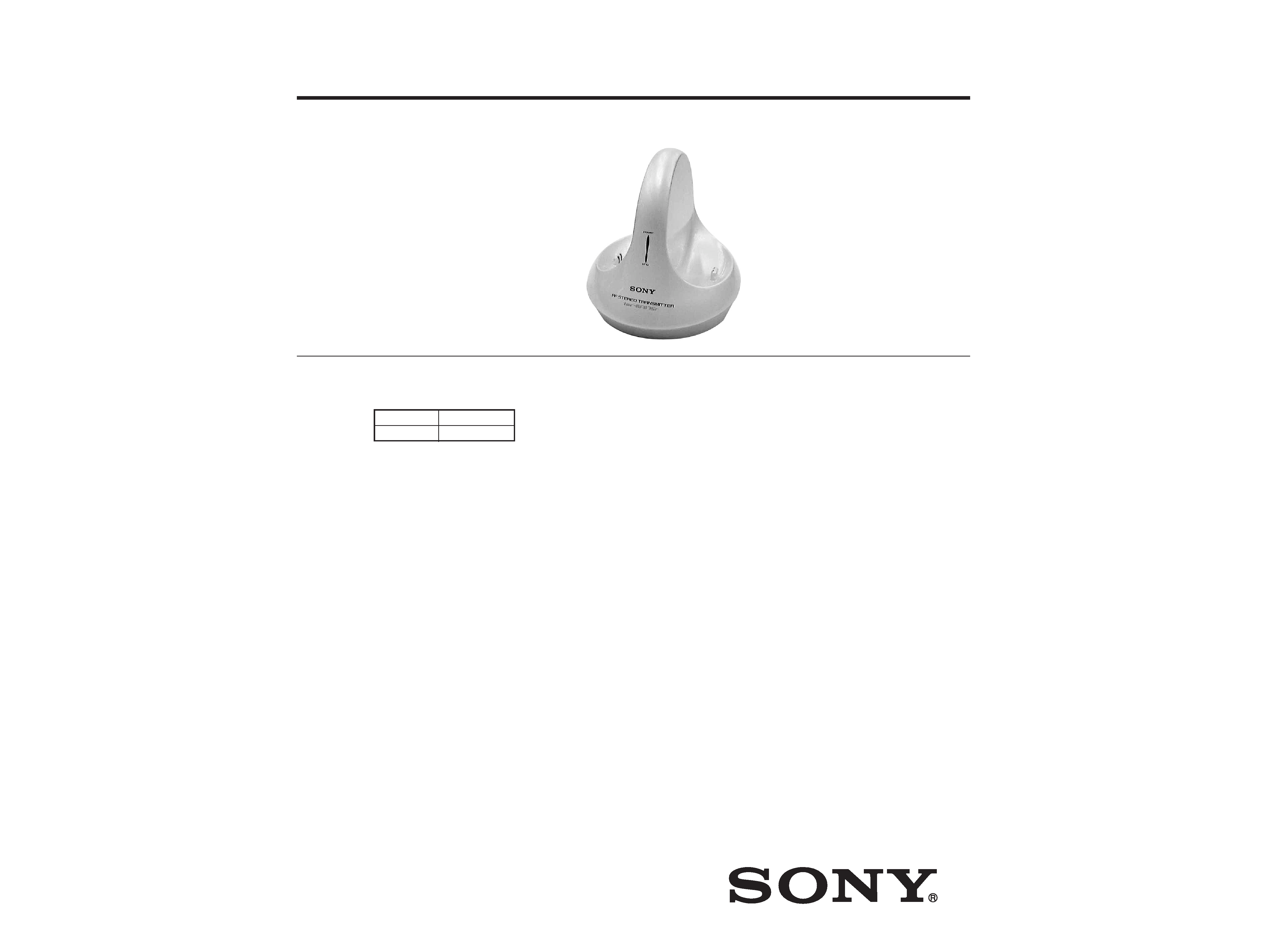
TMR-RF875R
AEP Model
UK Model
SERVICE MANUAL
TRANSMITTER
SPECIFICATIONS
Headphones
MDR-RF875R
Transmitter
TMR-RF875R
TMR-RF875R is the component model block one in the MDR-RF875RK.
COMPONENT MODEL NAME FOR MDR-RF875RK
General
Carrier frequency
863.5 864.5 MHz
Channel
Ch1, Ch2, Ch3
Modulation
FM stereo
Frequency response
18 22,000 Hz
Transmitter
Power source
DC 9 V: supplied AC power
adaptor
Audio input
phono jacks/stereo mini jack
Dimensions
Approx. 130
× 135 × 150 mm
(5 1/4
× 5 3/8 × 6 in.) (w/h/d)
Mass
Approx. 200 g (7 oz.)
Design and specifications are subject to change without
notice.
Ver 1.0 2000. 08
-- 2 --
SECTION 1
GENERAL
This section is extracted
from instruction manual.
DC IN 9V
OFF ON
FILTER
NOISE
12 3
CHANNEL
R
BA
L
AUDIO IN
Setting up the
transmitter
1 Connect the transmitter to audio/video
equipment. Select one of the hookups
below depending on the jack type:
A
To connect to a headphone jack
Transmitter
Left channel
(white)
Right channel
(red)
Unimatch plug
adaptor
(supplied)
CD Walkman,
MD Walkman,
WALKMAN*,
VCR, etc.
to headphones
jack (stereo
mini jack)
Connecting cord
(supplied)
to AUDIO IN
A jacks
to headphones
jack (stereo
phone jack)
Notes on chip component replacement
· Never reuse a disconnected chip component.
· Notice that the minus side of a tantalum capacitor may be
damaged by heat.
Flexible Circuit Board Repairing
· Keep the temperature of soldering iron around 270°C
during repairing.
· Do not touch the soldering iron on the same conductor of the
circuit board (within 3 times).
· Be careful not to apply force on the conductor when soldering
or unsoldering.
-- 3 --
SECTION 2
DISASSEMBLY
2-1. HOUSING (UPPER)
2-2. TX-BASE BOARD
Note :
Follow the disassembly procedure in the numerical order given.
2-3. CHG-NR BOARD
1
Four screws (P 2
× 8)
Housing (upper)
2
3
TX-BASE board
2
1
Screw (P 2
× 6)
Screw
Housing (upper)
Housing (upper)
2
CHG-NR board
1
Four screws (P 2
× 6)
-- 4 --
Setting :
SECTION 3
ELECTRICAL ADJUSTMENTS
Transmission Frequency Check
1. Set the noise filter SW to OFF.
2. Input a signal of 1 kHz, 40 mVrms to only the L-CH (J402).
3. Connect a telescopic antenna to the frequency counter input
and extend the antenna to a length of approximately 8 cm.
4. Place TX-BASE board close to the frequency counter, then mea-
sure the frequencies of CH1, CH2 and CH3 and make sure the
values are as follows:
CH1 : 863.5 MHz ± 40 kHz
CH2 : 864.0 MHz ± 40 kHz
CH3 : 864.5 MHz ± 40 kHz
When the frequency does not satisfy the specified value, ex-
change the vco unit. When completed with replacement, recheck
the frequecies of CH1, CH2 and CH3.
Compresser Output Check
1. Set the channel to CH2.
2. Input a signal of 1 kHz, 316 mVrms to L-CH and R-CH of J402.
3. Measure IC 601 pin 7 and IC 602 pin 7 on the CHG-NR board
using a digital voltmeter (AC range) and confirm the value is
100 mVrms ± 5mV (Fig.1).
4. Input a signal of 1 kHz, 31.6 mVtms to L-CH and R-CH of J402.
5. Measure IC 601 pin 7 and IC 602 pin 7 on the CHG-NR board
using a digital voltmeter (AC range) and confirm the value is
31.6 mVrms ± 5 mV (Fig.1).
6. When the frequency is not satisfied the specified value, exchange
TX- BASE board or CHG-NR board.
AF signal
generator
Telescopic
antenna
8 cm
L-CH / R-CH (J402)
TMR-RF875R
set
TMR-RF875R
set
Frequency counter
Pilot Signal and MPX Signal Modulation Check and
Adjustment
1. Set the channel to CH2.
2. No signal input (The operating time in this case is limited to 4
or 5 minutes.)
3. See the RV402 and RV403 to max. (clockwise)
4. Connect a digital voltmeter (AC range) to the movable terminal
of RV403 (Fig.2).
5. Adjust the value of the digital voltmeter to minimum by RV401.
6. See the RV402 to minimum. (counter clock wise)
7. Adjust the value of the digital voltmeter to max by L407.
8. Adjust the value of the digital voltmerter to 1.7 mVrms ± 0.1
mV by RV403.
9. Connect a digital voltmeter (AC range) with LPF to movable
terminal of RV403 (Fig.2).
10. Input a signal of 1 kHz, 316 mVrms to only the L-CH.
11. Adjust the value of the digital voltmeter to 2.5 mVrms ± 0.2
mV by RV402.
Connection points and Adjustment Location :
S402
J402
(L-CH) (R-CH)
CH3
CH2 CH1
VCO UNIT
RV403
RV402
RV401
L407
R464
IC 602
IC 601
1
8
4
5
1
8
4
5
CHG-NR board
+
digital
voltmeter
(AC range)
(Fig. 1)
7 pin
RV401-403,
L407
Modulation
check and
adjustment.
+
digital
voltmeter
(AC range)
(Fig. 2)
R464
TMR-RF875R
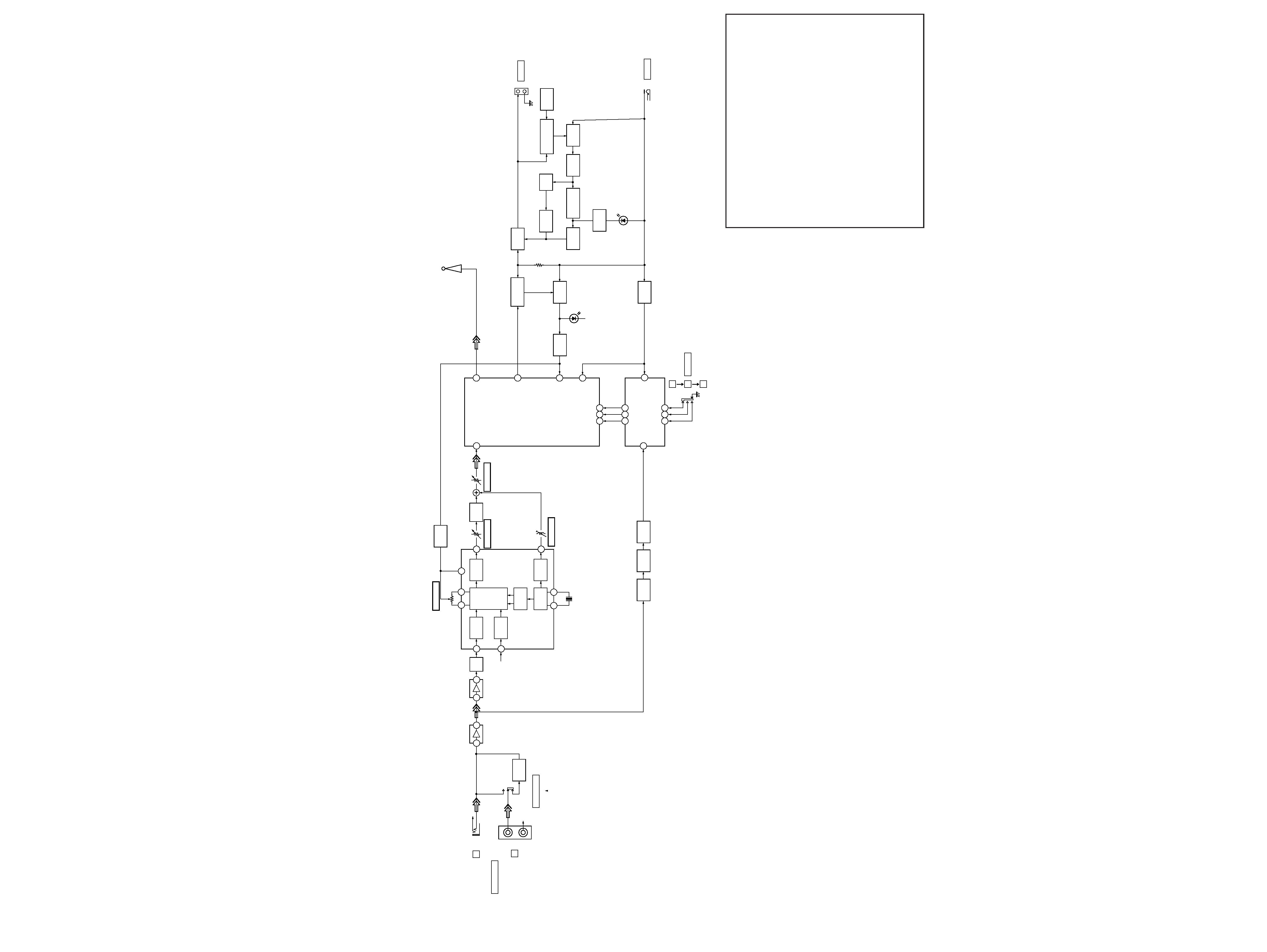
4-1. BLOCK DIAGRAM
-- 5 --
-- 6 --
SECTION 4
DIAGRAMS
Note on Printed Wiring Board:
· X : parts extracted from the component side.
· b : Pattern from the side which enables seeing.
Note on Schematic Diagram:
· All capacitors are in µF unless otherwise noted. pF: µµF 50 WV or
less are not indicated except for electrolytics and tantalums.
· All resistors are in
and 1/4 W or less unless otherwise specified.
·
¢
: internal component.
· A : B+ Line.
· H : adjustment for repair.
· Power voltage is dc 9 V and fed with regulated dc power supply
from battery terminal.
· Voltages are dc with respect to ground under no-signal conditions.
· Voltages are taken with a VOM (Input impedance 10 M
).
Voltage variations may be noted due to normal production toler-
ances.
· Waveforms are taken with a oscilloscope.
Voltage variations may be noted due to normal production toler-
ances.
· Circled numbers refer to waveforms.
· Signal path.
L: AUDIO
J401
S401
NOISE FILTER
NOISE
FILTER
CH1
AMP
BUFFER
BUFFER
Q401
RECT
D404,405
2V
D408
INPUT
DET
DIVIDER
BUFFER
OSC
AMP
TIME
DEVISION
MPX
AUDIO IN
B
J402
A
OFF
|
ON
S402
CHANNEL
L
R
R-CH
R-CH
R-CH
14
12
11
9
8
13
10
12
11
6
7
9
15
7
6
CH2
AMP
1
X401
38kHz
RV402
RV401
L407
RV403
MOD IN
CE DI CL
CE DI CL
VS
16
5V
VCO CONTROLLER
IC404
IC401
IC601
SWITCH
Q403
LPF
IC403
STEREO MPX
IC405(1/2)
IC405(2/2)
+5V
REG
SWITCH
Q404
SWITCH
Q601
SWITCH
Q602
SWITCH
Q604
SWITCH
Q603
OSC
Q605
+4V
Q402
REF V
POWER OFF
DET
IC604(2/2)
DETECT
IC402
+5V
REG
IC605
COMPARATOR
IC603
DETECT
IC604(1/2)
ANT
5V
B+
T-OUT
ANT401
D401
D402
J404
DC IN 9V
CHARGE
(power)
(chg)
1
2
3
VCO UNIT
MODULATION
MODULATION
MODULATION
MODULATION
7
2
1
13
· R-ch is omitted due to same as L-ch.
· Signal path.
L
: AUDIO
16