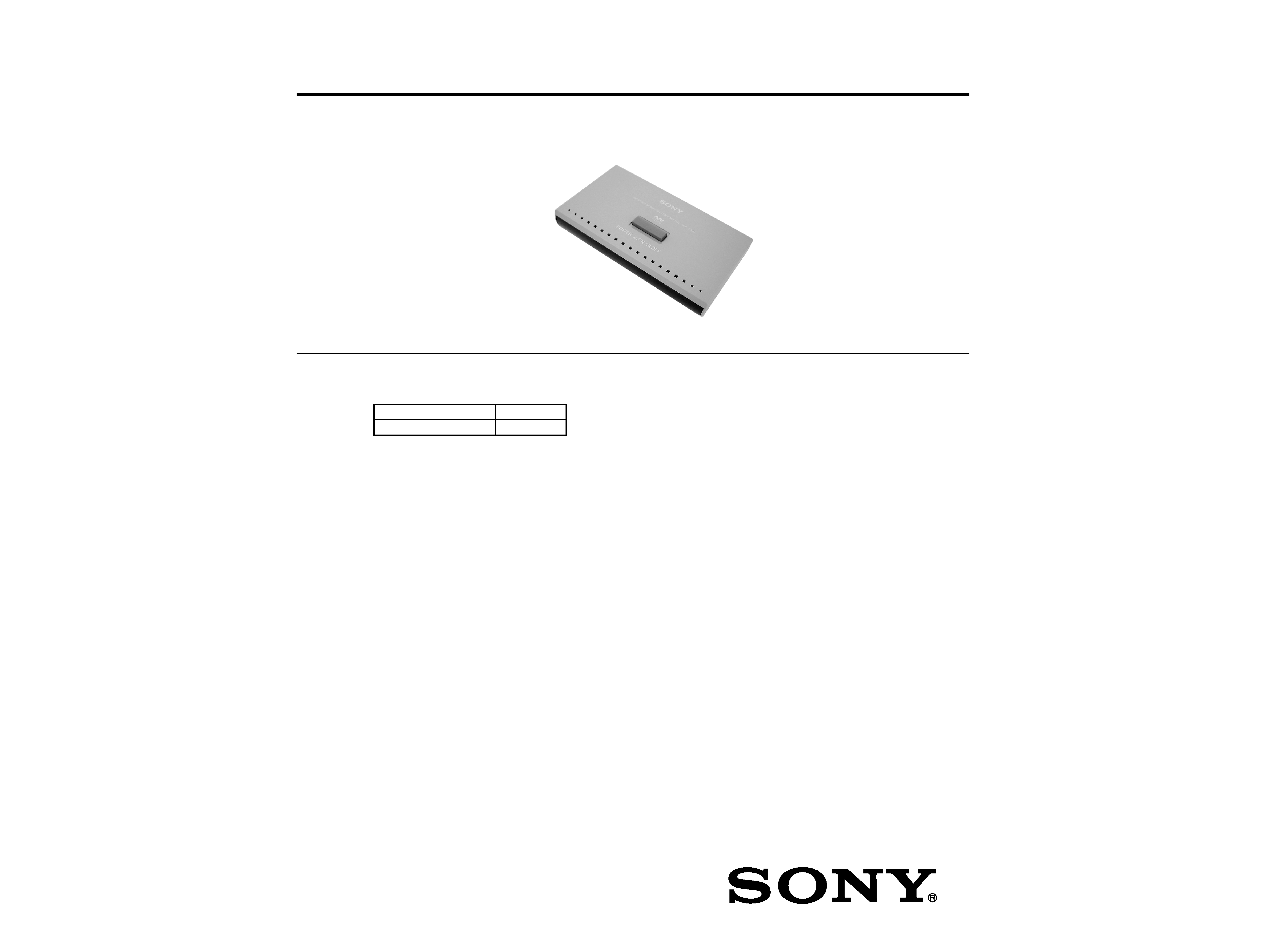
SERVICE MANUAL
US Model
TMR-IF10M
SPEAKER REMOTE
COMMANDER SYSTEM
· TMR-IF10M is the component model block one in RM-VS10TV.
COMPONENT MODEL NAME FOR RM-VS10TV
TRANSMITTER
TMR-IF10M
REMOTE COMMANDER
RM-VS10
General
Modulation system
Frequency modulation
Carrier frequency
2.3 MHz (monaural)
Transmitter TMR-IF10M
Power source
DC IN 9 V jack accepts power supplied
from the AC power adaptor for use on
120 V AC, 60 Hz voltage.
Input
Internal microphone or phone jack/stereo
mini jack
SPECIFICATIONS
Notes on Chip Component Replacement
· Never reuse a disconnected chip component.
· Notice that the minus side of a tantalum capacitor may be
damaged by heat.
Signal connection range
Maximum: 7 m* (23 ft.) (when the Commander
is facing directly toward the transmitter)
Dimensions
130
× 38 × 70 mm (5 1/8 × 1 1/2 × 2 7/8 in.)
(w
× h × d)
Mass
Approx. 100 g (4 oz.)
* The distance may vary depending on using conditions and
the manufacturer and equipment that is used.
Design and specifications are subject to change without
notice.
Ver 1.0 2000. 06
2
1
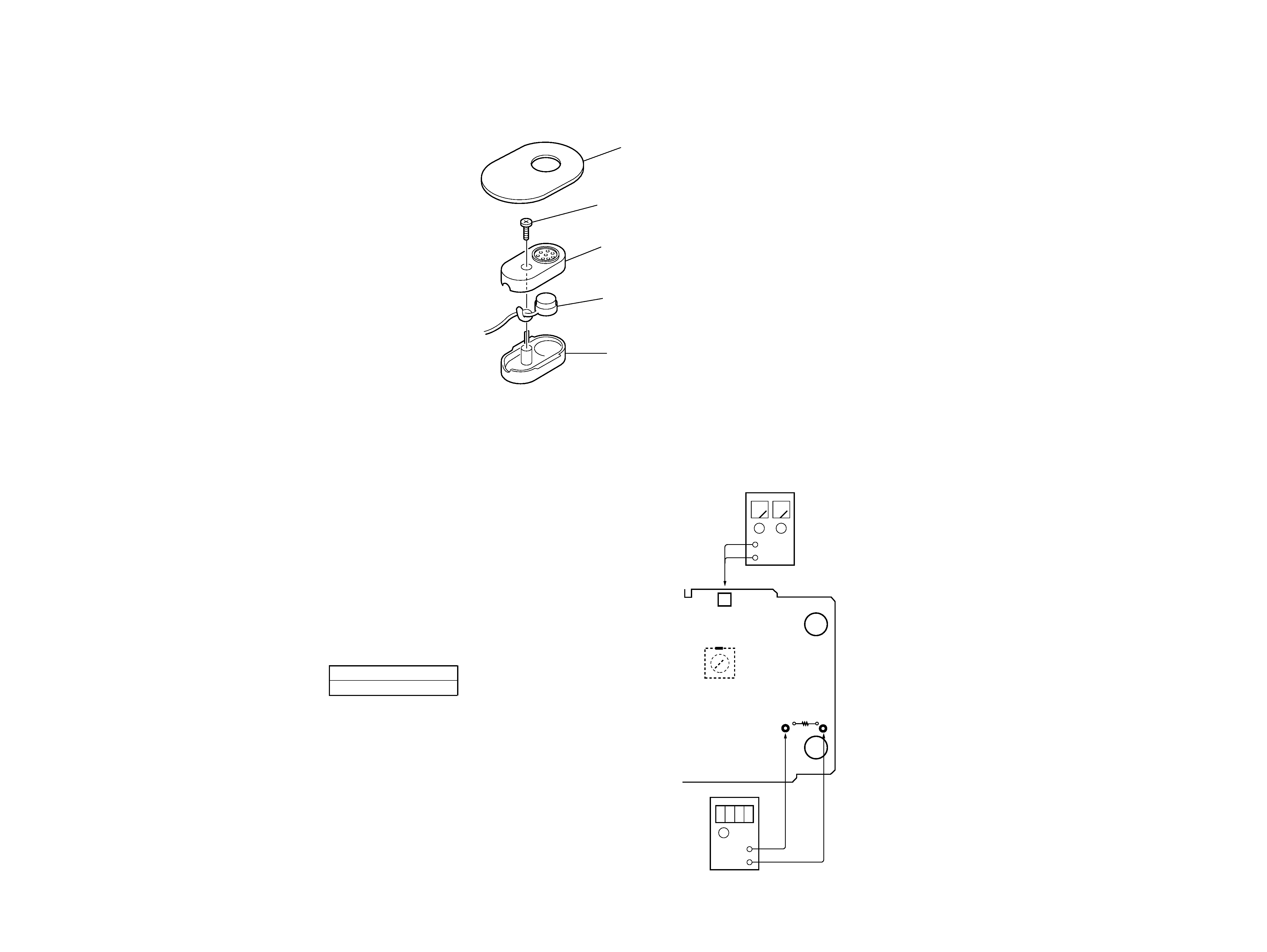
sheet, microphone fixed
2
B 2x6
3
case (A), microphone
4
case (B), microphone
5
microphone, electret condenser
SECTION 2
ELECTRICAL ADJUSTMENTS
Note:
1. The adjustments is performed in the order that they are listed.
2. When adjusting the remote commander, the transmitter is used
for adjustment.
3. 0 dB=1.0 V
2-1. Transmitter
2-1-1. Oscillating frequency adjustment
Method:
1. Supply 9 V to the DC jack (J1) from a stabilized power supply.
2. Perform this adjustment without signal.
3. Connect a frequency counter between TP17 (RF) and TP18
(GND).
4. Adjust L1 so that the reading on the counter is 2,300 kHz.
Specified Value:
Frequency counter
2,295 to 2,305 kHz
5. Connect an oscilloscope between TP17 (RF) and TP18 (GND).
6. Verify that the Vp-p value of the waveform on the oscilloscope is
1.2 V or more.
Connections and adjustment element:
Note : Follow the disassembly procedure in the numerical order given.
1-1. MICROPHONE, ELECTRET CONDENSER (MIC1)
SECTION 1
DISASSEMBLY
TP17
L1
J1
9Vdc
TP18
R32
TX BOARD
(CONDUCTOR SIDE)
+
+
Stabilized power suppy
Frequency counter
and
Oscilloscope
TMR-IF10M
3
4
3-1. BLOCK DIAGRAM
SECTION 3
DIAGRAMS
THIS NOTE IS COMMON FOR PRINTED WIRING
BOARDS AND SCHEMATIC DIAGRAMS.
(In addition to this, the necessary note is
printed in each block.)
for Schematic Diagram:
· All capacitors are in µF unless otherwise noted. pF: µµF
50 WV or less are not indicated except for electrolytics
and tantalums.
· All resistors are in
and 1/4 W or less unless otherwise
specified.
·
%
: indicates tolerance.
·
f
: internal component.
· C : panel designation.
· U : B+ Line.
· H : adjustment for repair.
· Power voltage is dc 9 V and fed with regulated dc power
supply from external power voltage jack.
· Voltage is dc with respect to ground under no-signal
(detuned) condition.
no mark : POWER on
· Voltages are taken with a VOM (Input impedance 10 M
).
Voltage variations may be noted due to normal produc-
tion tolerances.
· Signal path.
F
: Analog
J
: RF
for Printed Wiring Boards:
· X : parts extracted from the component side.
·
f
: internal component.
· b : Pattern from the side which enables seeing.
TX BOARD
A
B
9
H
L
10
8
11
NOR
IC1
J2
J3
J4
R
L
AUDIO
IN
MIC1
04
2
3
8
5
7
ALC AMP
IC2
OSC
L1, Q2
L1
OSCILLATION
FREQUENCY
REG
Q1
LED DRIVER
Q3, 4
INFRARED
EMITTER
D4-7
B+
SW1
B+
J1
DC IN 9V
· Signal path
: ANALOG
: RF
!
POWER
ON
OFF
5
6
TMR-IF10M
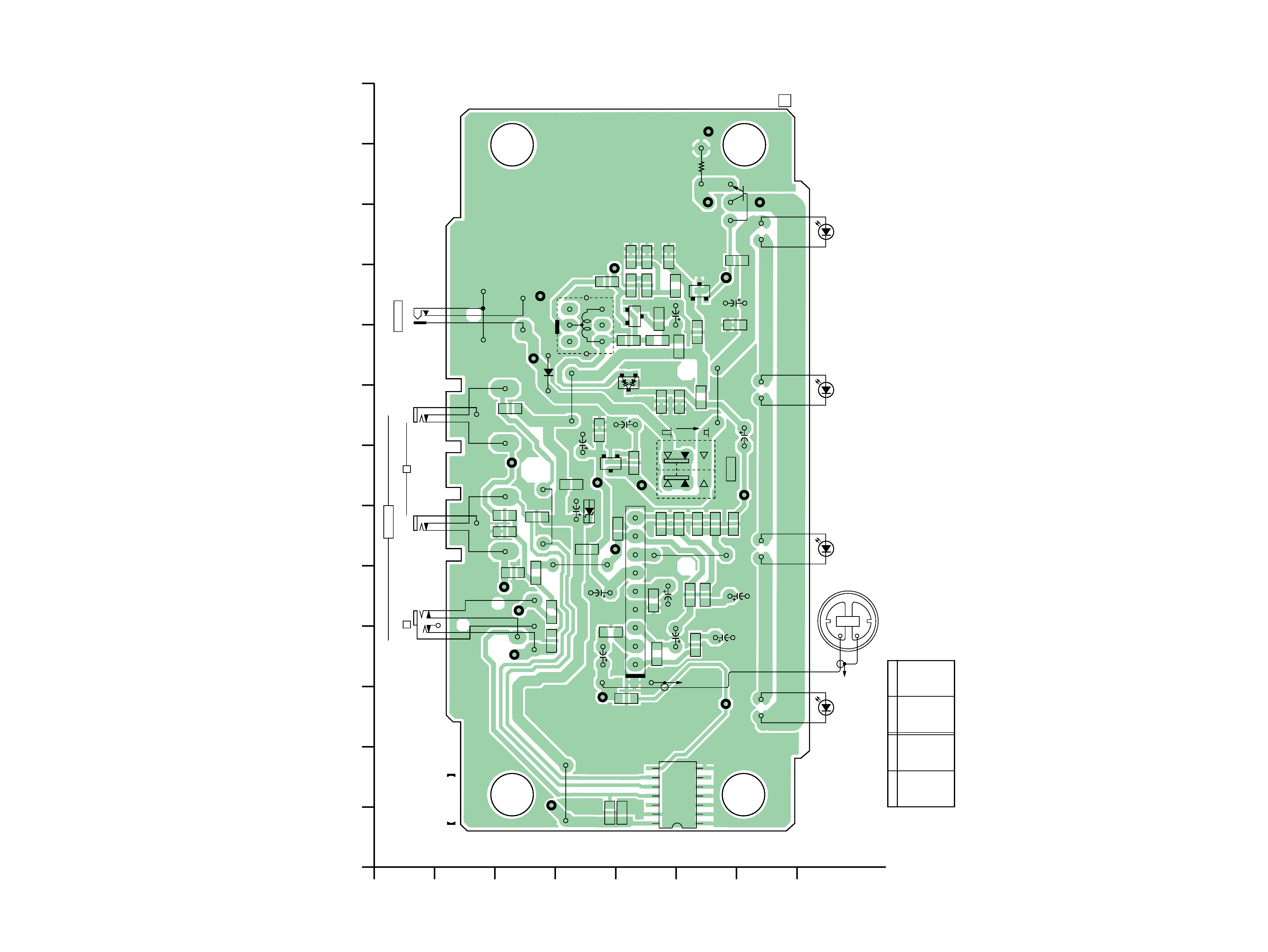
3-2. PRINTED WIRING BOARD · Refer to page 4 for Note.
D1
C-9
D2
D-6
D3
E-8
D4
H-11
D5
H-8
D6
H-6
D7
H-3
· Semiconductor Location
Ref. No.
Location
Ref. No.
Location
IC1
E-2
IC2
E-5
Q1
D-7
Q2
E-10
Q3
F-10
Q4
F-12
R11
R13
C3
R19
C13
R18
C14
R21
C17
R22
C26
C21
R27
R28
R30
C22
C20
C19
R29
R25
R1
C12
R17
C11
C6
C15
C10
R14
R20
R16
R15
R5
C25
C8
R34
R35
R23
C24
R31
C7
C18
R24
C23
R26
R9
R33
R10
R3
R2
R4
C5
Q1
R12
IC1
14
8
17
JW4
JW7
C16
TP13
D2
C4
C2
TP12
TP3
C1
C9
D3
JW3
1
E
B
E
C
B
C
23
64
L1
TP14
TP17
TP18
TP15
TP16
Q2
Q4
Q3
TP4
TX BOARD
TP7
TP11
TP8
TP10
JW2
TP6
TP2
JW6
JW1
TP9
TP1
D1
TP5
J4
B
A
J3
L
J2
R
AUDIO IN
MIC1
04
D7
D6
D4-7
INFRARED EMITTER
D5
D4
1-676-031-
11
R32
SW1
19
J1
DC IN 9V
IC2
C
BE
!
POWER
ON
OFF
1
A
B
C
D
E
F
G
H
2
3
4
5
6
7
8
9
10
11
12
13
TMR-IF10M
7
8
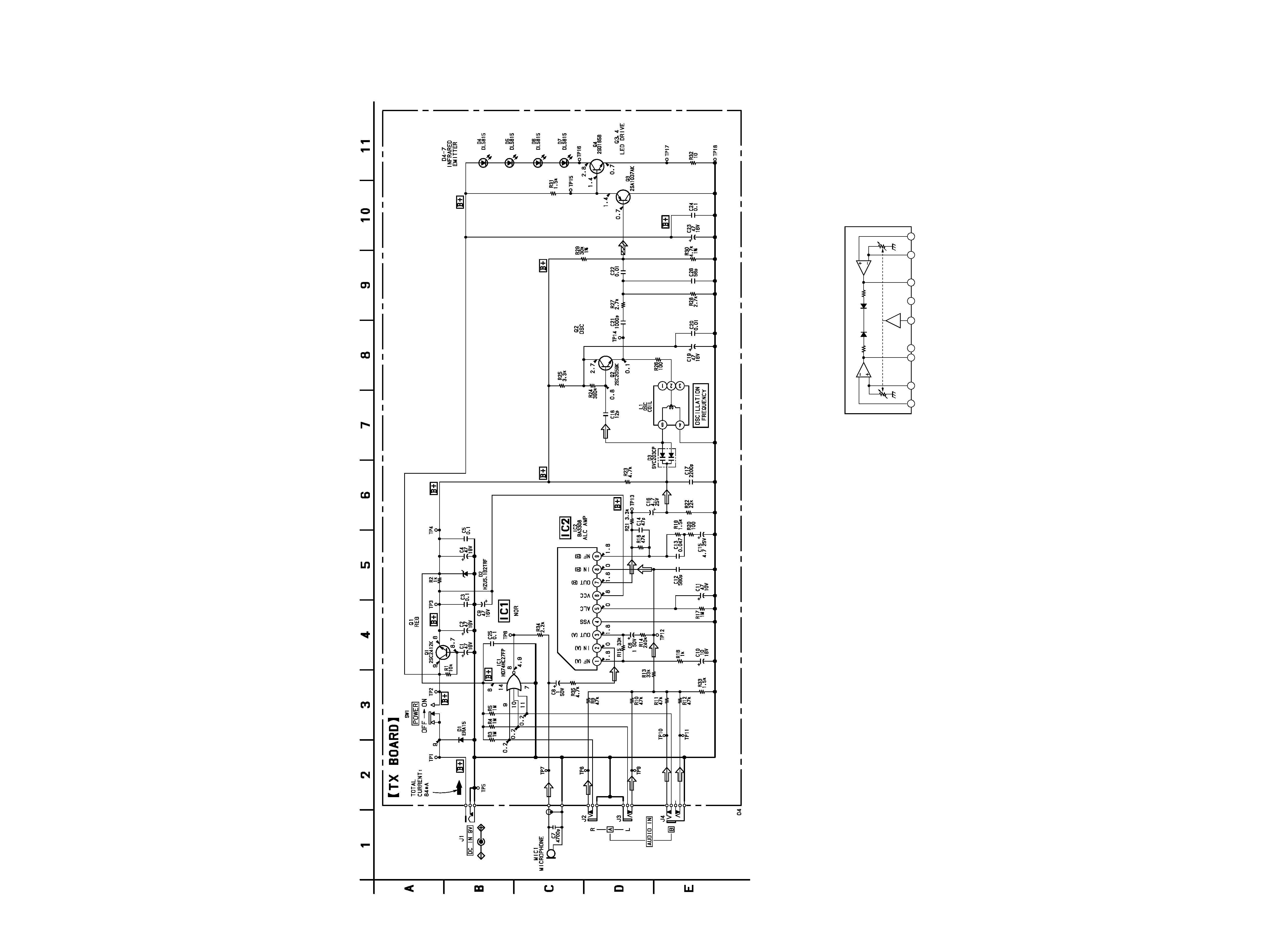
3-3. SCHEMATIC DIAGRAM · Refer to page 4 for Note.
· IC BLOCK DIAGRAMS
IC2 BA3308
3
2
1
4
5
6
7
8
9
NF
IN
VSS
OUT
ALC
VCC
OUT
IN
NF