1
AEP Model
UK Model
E Model
SPECIFICATIONS
SERVICE MANUAL
MICRO Hi-Fi COMPONENT SYSTEM
ST-SP55
FM stereo, FM/AM superheterodyne tuner
Input
AUX IN (phono jacks):
voltage 250 mV, impedance
47 kilohms
Output
AUX OUT (phono jacks): voltage 250 mV, impedance
1 kilohm
FM tuner section
Tuning range
87.5 108.0 MHz
(50 kHz step)
Aerial
FM lead aerial
Aerial terminals
300 ohms unbalanced
Intermediate frequency
10.7 MHz
AM tuner section
Tuning range
European model:
531 1,602 kHz
(with the interval set at 9 kHz)
Other models:
531 1,602 kHz
(with the interval set at 9 kHz)
530 1,710 kHz
(with the interval set at 10 kHz)
Aerial
AM loop aerial
External aerial terminals
Intermediate frequency
450 kHz
General
Dimensions (w/h/d) incl. projecting parts and controls
Approx. 202
× 75 × 291 mm
Mass
Approx. 1.3 kg
Design and specifications are subject to change
without notice.
ST-SP55 is the tuner section
in CMT-SP55MD or CMT-SP55TC.

2
SAFETY-RELATED COMPONENT WARNING !!
COMPONENTS IDENTIFIED BY MARK 0 OR DOTTED LINE
WITH MARK 0 ON THE SCHEMATIC DIAGRAMS AND IN
THE PARTS LIST ARE CRITICAL TO SAFE OPERATION.
REPLACE THESE COMPONENTS WITH SONY PARTS
WHOSE PART NUMBERS APPEAR AS SHOWN IN THIS
MANUAL OR IN SUPPLEMENTS PUBLISHED BY SONY.
TABLE OF CONTENTS
1. SERVICE NOTE .................................................... 3
2. GENERAL .......................................................................... 3
3. DIAGRAMS
3-1. Circuit Boards Location ........................................................ 4
3-2. Block Diagram ...................................................................... 5
3-3. Schematic Diagram Main Section .................................. 6
3-4. Printed Wiring Board Main Section ................................ 7
3-5. Schematic Diagram Panel Section .................................. 8
3-6. Printed Wiring Board Panel Section ................................ 9
3-7. IC Pin Functions .................................................................. 10
3-8. IC Block Diagram ............................................................... 11
4. EXPLODED VIEW
4-1. Case and Front Panel .......................................................... 12
5. ELECTRICAL PARTS LIST ........................................ 13
3
SECTION 2
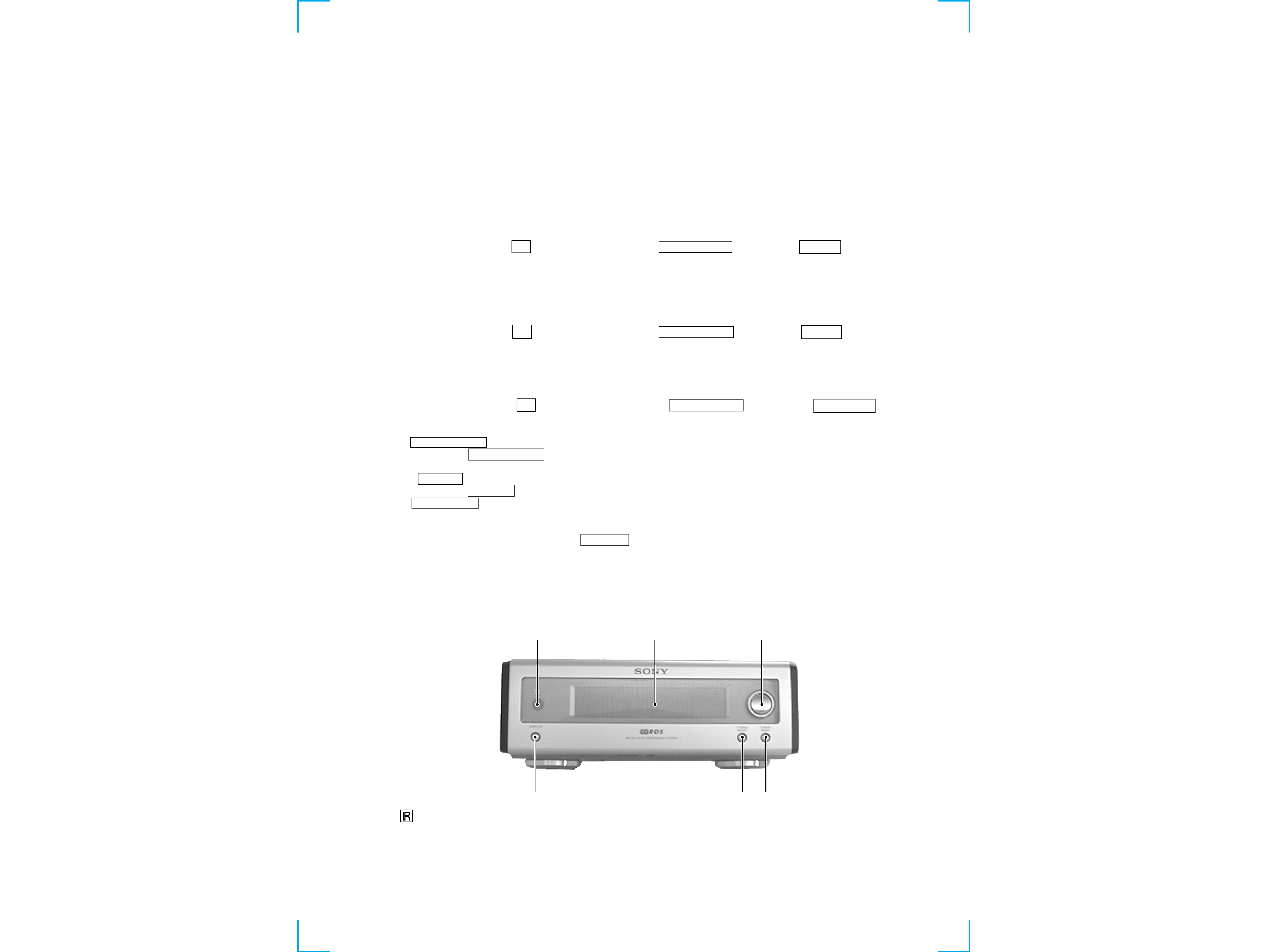
GENERAL
1
(Remote sensor)
2
Display window
3
TUNING +/ button
4
TUNER/BAND button
5
TUNING MODE button
6
DISPLAY button
1
6
5
4
2
3
SECTION 1
SERVICE NOTE
CD Text Display
· This unit displays CD text.
Text is displayed for the first 50 track only and will not be displayed from the 51st track onwards. Do not suspect a fault in this case.
In some cases, some special characters will not be displayed and may be replaced by other characters. Do not suspect a fault in this case.
Cold Reset
· The cold reset clears all data including preset data stored in the RAM to initial conditions. Execute this mode when returning the set to the
customer.
Procedure :
1. When the power ON, press the ?/1 button (TA) while pressing the TUNING MODE button (ST) and ML buttons (CDP) together.
2. "COLD RESET" is displayed on the fluorescent indicator tube and reset is executed.
Hot Reset
· This mode reset the preset data kept in the memory. The hot reset mode functions same as if the power cord is plugged in and out.
Procedure :
1. When the power ON, press the ?/1 button (TA) while pressing the TUNING MODE button (ST) and lm buttons (CDP) together.
2. Turn off the unit and reset is executed.
GC Test Mode
Procedure :
1. When the power ON, press the ?/1 button (TA) while pressing the TUNING MODE button (ST) and PLAY MODE buttons (CDP)
together.
2. LCD are all turned on.
3. Press TUNING MODE button (ST) to enter the model destination indecation mode. "SP55
CE2" or "SP55
ASIA2" appears.
4.
Every pressing of TUNING MODE button (ST) changes the display in the following order.
MC Version
t CD Version t ST Version t TC Version t TA Version t TM Version t model destination display.
5.
Press DISPLAY button (ST) and the date appears as " 00615a "
Every pressing of DISPLAY button (ST) changes the display in the Version display and model destination display.
6. Press TUNER/BAND button (ST) to enter the key check mode.
7. In the key check mode, the fluorescent indicator tube displays "Key 0 Vol 0". Each time a button is pressed, "Key" value increases.
However, once a button is pressed, it is no longer taken into account.
"Vol" Value increases like "1, 2, 3 ..." if rotating VOLUME knob (TA) in the clockwise direction, or decreases like "0, 9, 8 ..." if rotating
in the counterclockwise diretion.
8. To exit from this mode, disconnect the power cord.
This unit cannot be repaired by itself.
When repairing, connect the whole system except for the speaker.
4
SECTION 3
DIAGRAMS
THIS NOTE IS COMMON FOR PRINTED WIRING
BOARDS AND SCHEMATIC DIAGRAMS.
(In addition to this, the necessary note is printed
in each block.)
For schematic diagrams.
Note:
· All capacitors are in µF unless otherwise noted. pF: µµF
50 WV or less are not indicated except for electrolytics
and tantalums.
· All resistors are in
and 1/4 W or less unless otherwise
specified.
·
f
: internal component.
· C : panel designation.
For printed wiring boards.
Note:
· X : parts extracted from the component side.
· Y : parts extracted from the conductor side.
·
a
: Through hole.
· b : Pattern from the side which enables seeing.
(The other layers' patterns are not indicated.)
· U : B+ Line.
· V : B Line.
· H : adjustment for repair.
· no mark : FM
: Can not be measured.
· Voltages are taken with a VOM (Input impedance 10 M
).
Voltage variations may be noted due to normal produc-
tion tolerances.
· Waveforms are taken with a oscilloscope.
Voltage variations may be noted due to normal produc-
tion tolerances.
· Circled numbers refer to waveforms.
· Signal path.
F
: FM
J
: CD
d
: TAPE
G
: REC (TAPE/MD)
j
: MD
· Abbreviation
MY
: Malaysia model.
SP
: Singapore model.
HK
: Hong Kong model.
KR
: Korea model.
AED
: North European model.
· Indication of transistor
C
These are omitted
E
B
Q
C
These are omitted
E
B
Note:
The components identified by mark 0 or
dotted line with mark 0 are critical for
safety.
Replace only with part number specified.
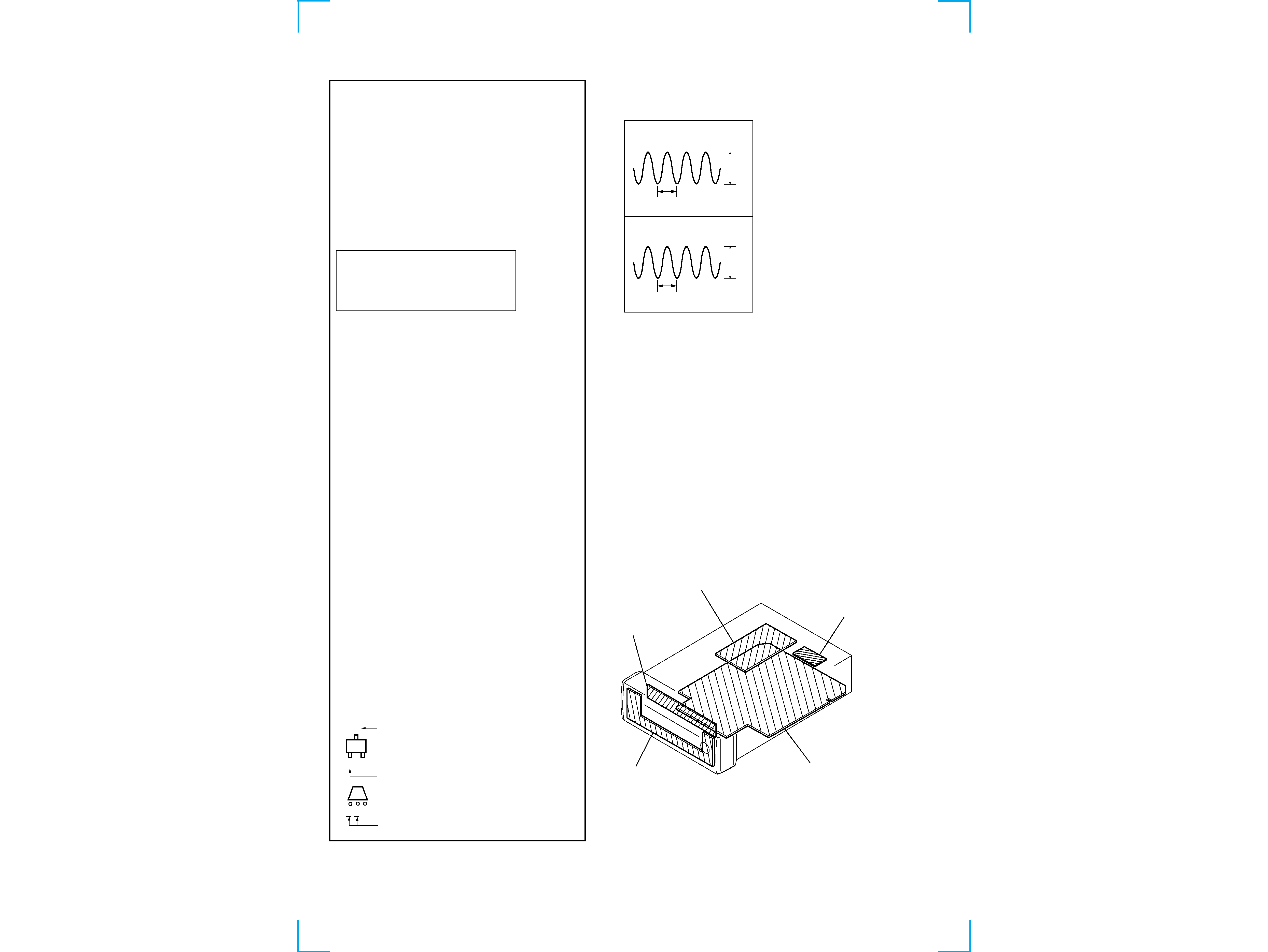
1 IC701 qa XCOUT
2 IC701 qd XOUT
30.5
µsec
100nsec
2.7Vp-p
4.6Vp-p
· WAVEFORMS
MAIN BOARD
MAIN board
PANEL board
LED board
PIN JACK board
tuner unit (FM/AM)
3-1. CIRCUIT BOARDS LOCATION
ST-SP55
5
5
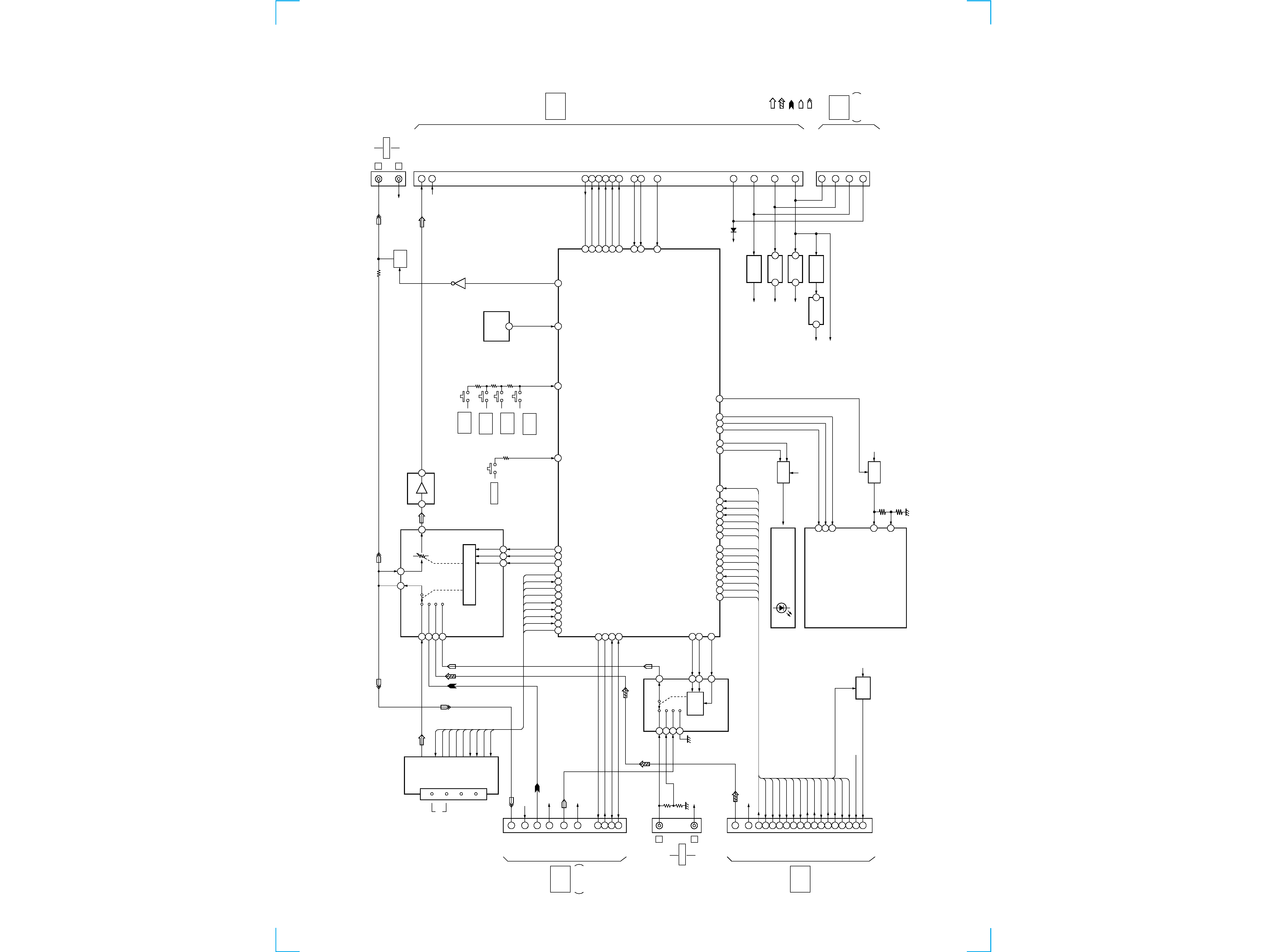
3-2. BLOCK DIAGRAM
: FM
: CD
: MD
: TAPE
: REC (TAPE/MD)
· Signal Path
· R-ch is omitted due to same as L-ch.
Q291
+10V REG
75
61
VOL-DA
TA
FUNC1
60 FUNC2
58
13
FUNC INHIBIT
72
DSG-OFF
76
PRE-MUTE
77
HP-MUTE
HP-MUTE
78
TA-STANDBY
79
PWR-RELAY
80
SP-RELAY
86
VOL-ENC-A
87
VOL-ENC-B
DSG-OFF
XPRE-MUTE
ON/STBY
P-RELAY
S-RELAY
ENC0
ENC1
TA-KEY
X0
X1
X2
X3
AUXH-L
AUXL-L
TC-L
74
VOL-CLK
73
VOL-LA
T
14
13
12
11
DI
CONTROL
CL
CE
44
P
AUSE-LED
43
PLA
Y
-LED
42
CD-XL
T
41
SENSE
40
LOAD-IN
39
LOAD-OUT
38
BD-POWER
37
CD-CLK
35
CD-DA
TA
34
LPC-HOLD
33
SQCLK
32
SQDA
TA
19
SCOR
95
CDM-SW
92
KEY3
91
KEY2
LED1
LED0
CD-XLA
T
SENS
LOAD-OUT
LOAD-IN
CD-POWER
CD-CLK
CD-DA
TA
HOLD
SQCK
SQSO
SCOR
CDM-SW
CD-KEY
P-DOWN OUT
PCPON
IIC-DAT
IIC-CLK
10
9
10
9
6
17
6
8
1
6
4
8
2
5
1
11
10
14
12
3
5
6
7
8
9
10
11
12
13
14
15
16
17
18
19
4
11
10
13
9
12
15
16
14
4
5
1
3
17
16
19
15
12
14
15
11
5
3
1
BUFFER
IC231
Q201
Q221
MUTE
1 30 2
51
RO-MUTE
AUX
Q301
+11V REG.
3
2
IC282
-7V REG.
IC281
+7V REG.
3
1
IC283
+5V REG.
3
1
L
R
AUX OUT
L
R
AUX IN
+5V
SWITCH
Q281,282
CD L
IIC-CLK
IIC-DATA
PCPON
PDOWN
TC-R
TC-L
MD-R
MD-L
REC R
REC L
CD R
CDKEY
PLAY LED
PAUSE LED
DATA
XLAT
CLOK
HOLD
SQSO
SENS
SQCK
SCOR
CD MSW
LOAD-IN
LOAD-OUT
CD-KEY
LED0
LED1
CD-DATA
CD-XLAT
CD-CLK
HOLD
SQSO
SENS
SQCK
SCOR
CDM-SW
CD-PWR
+ UBREG(L)
LOAD-IN
LOAD-OUT
UNREG(L)
+5V
SYSTEM
CONTROL
2
(TO CDP-SP55)
SYSTEM
CONTROL
1
(FROM TA-SP55)
SYSTEM
CONTROL
3
SYSTEM
CONTROL
3
TO TC-SP55/
MDS-SP55
TO TC-SP55/
MDS-SP55
CN203(1/2)
J210(2/2)
CN203(2/2)
CN201
J210(1/2)
CN205
+UNREG(L)
+UNREG(L)
-UNREG
+13.5V(REG)
+5.6V(UNSW)
TA-KEY/HPSW
ENC1
ENC0
XS-RELAY
P-RELAY
ON/STBY/AMP-MUTE
HP-MUTE
XPRE-MUTE
R
L
DSG-OFF
-UNREG(L)
+UNREG(H)
D+5.6V(UNSW)
LSELO
LIN
LOUT
IC401
INPUT SELECT/EVR
ST-L
L1
L2
L3
L4
MD-L
CD-L
SEL-L
R-CH
R-CH
R-CH
R-CH
+5V
R-CH
R-CH
R-CH
PDOWN
PCPON
DATA
CLK
IC701
MASTER
CONTROL
+10V
-7V
+7V
+5V
+5V
+UNREG(L)
CONTROL
X
A
B
INH
IC202
INPUT SELECTOR
09
D950-957
6
5
4
DATA
SCK
STB
1
VDD
3
VREF
1
OUT
DPDATA
DPCLK
DPCS
LCD
DISPLAY
UNIT
IC901
REMOTE
COMMANDER
RECEIVER
B+
SWITCH
LED
DRIVE
+5V
+5V
Q704
Q701,702
Q705,706
7V
BACK
LIGHT
ILL(-7V)
84 4
DP
PWR
BL
DIMMER
1 2 3
DP
DA
TA
DP
CLK
DP
CS
83
DP
PWR
88
SIRCS
89
90
KEY0
KEY1
21
20
24
23
27
18
26
28
25
RDS
DA
TA
RDS
INT
TUNED
STEREO
ST
MUTE
ST
DIN
ST
DOUT
ST
CLK
ST
CE
S923
S922
S921
S920
S910
TUNING
MODE
TUNING
TUNER/
BAND
TUNING
+
DISPLAY
85
67
30
29
TUNER
UNIT
RDS DATA
RDS INT
TUNED
STEREO
ST MUTE
ST DIN
ST DOUT
ST CLK
ST CE
FM 75
G
AM