SERVICE MANUAL
FM STEREO FM/AM RECEIVER
SPECIFICATIONS
STR-DA9000ES
Ver 1.2 2004.09
9-961-292-03
Sony Corporation
2004I05-1
Audio Group
© 2004.09
Published by Sony Engineering Corporation
US Model
Canadian Model
Continued on next page
This receiver incorporates Dolby* Digital and Pro
Logic Surround and the DTS** Digital Surround
System.
*Manufactured under license from Dolby
Laboratories.
"Dolby", "Pro Logic" and the double-D symbol are
trademarks of Dolby Laboratories.
** "DTS", "DTS-ES Extended Surround", and
"Neo:6" are trademarks of Digital Theater Systems,
Inc.
AUDIO POWER SPECIFICATIONS
POWER OUTPUT AND TOTAL HARMONIC
DISTORTION:
(Models of area code US only)
With 8 ohm loads, both channels driven, from 20
20,000 Hz; rated 170 watts per channel
minimum RMS power, with no more than
0.09% total harmonic distortion from 250
milliwatts to rated output.
Amplifier section
POWER OUTPUT
Rated Power Output at Stereo Mode
(8 ohms, 20 Hz 20 kHz, THD 0.15%)
200 W + 200 W
(4 ohms, 20 Hz 20 kHz, THD 0.15%)
220 W + 220 W
Reference Power Output
(8 ohms, 1 kHz, THD 0.09%)
FRONT1): 200 W + 200 W
CENTER1): 200 W
SURR1): 200 W + 200 W
SURR BACK1): 200 W + 200 W
(4 ohms, 1 kHz, THD 0.09%)
FRONT1): 220 W + 220 W
CENTER1): 220 W
SURR1): 220 W + 220 W
SURR BACK1): 220 W + 220 W
1) Depending on the sound field settings and the
source, there may be no sound output.
Frequency response
Inputs (Analog)
2) Input shorted and sealed at VOL MAX.
3) Weighted network + 20 kHz LPF, input level.
Inputs (Digital)
Outputs
EQUALIZER
PHONO
RIAA equalization curve
±0.5 dB
Power Amp Block
10 Hz 50 kHz
± 3 dB (8 ohms)
PHONO
Sensitivity: 3.5 mV
Impedance: 50 kilohms
S/N2): 90 dB (A, 40 mV
3))
CD/SACD, TAPE,
MD/DAT, DVD, LD,
TV/SAT, VIDEO 1, 2,
3, 4, 5
Sensitivity: 170 mV
Impedance: 50 kilohms
S/N2): 100 dB (A, 2 V3))
CD/SACD, DVD, LD,
VIDEO 1, TV/SAT
(Coaxial)
Impedance: 75 ohms
S/N: 100 dB
(A Network, 20 kHz LPF)
CD/SACD, DVD, LD,
TV/SAT, MD/DAT,
VIDEO1, 3 (Optical)
S/N: 100 dB
(A Network, 20 kHz LPF)
TAPE, MD/DAT
(REC OUT), VIDEO
1, 2, 3 (AUDIO OUT)
Voltage: 170 mV
Impedance: 2.2 kilohms
FRONT L/R,
CENTER,
SURROUND L/R,
SURROUND BACK
L/R, SUB WOOFER
Voltage: 2 V
Impedance: 220 ohms
Gain levels
±10 dB, 1 dB step

2
STR-DA9000ES
SAFETY-RELATED COMPONENT WARNING!!
COMPONENTS IDENTIFIED BY MARK 0 OR DOTTED
LINE WITH MARK 0 ON THE SCHEMATIC DIAGRAMS
AND IN THE PARTS LIST ARE CRITICAL TO SAFE
OPERATION. REPLACE THESE COMPONENTS WITH
SONY PARTS WHOSE PART NUMBERS APPEAR AS
SHOWN IN THIS MANUAL OR IN SUPPLEMENTS PUB-
LISHED BY SONY.
4) You can change the AM tuning scale to 9 kHz or 10
kHz. After tuning in any AM station, turn off the
receiver. While holding down PRESET TUNING +
or TUNING +, press ?/1. All preset stations will be
erased when you change the tuning scale. To reset
the scale to 10 kHz (or 9 kHz), repeat the procedure.
Video section
Inputs/Outputs
Video:
1 Vp-p, 75 ohms
S-video:
Y: 1 Vp-p, 75 ohms
C: 0.286 Vp-p, 75 ohms
COMPONENT VIDEO:Y: 1 Vp-p, 75 ohms
PB/CB/B-Y: 0.7 Vp-p, 75
ohms
PR/CR/R-Y: 0.7 Vp-p, 75
ohms
i.LINK section
Pin
4 pins
Transmission speed
S200 (Maximum data
transmission speed 200
Mbps)
Transmission protocol A/M transmission protocol
Format (input)
Super Audio CD* (DSD
PLAIN)
2 channel linear PCM (IEC-
60958-3)
Sampling frequency: 44.1
kHz
*Conforms to the copy protection technology of
DTLA (Revision 1.2).
General
Power requirements
120 V AC, 60 Hz
Power consumption
600 W
Power consumption (during standby mode)
1 W
AC outlets
1 switched, 120 W/1A MAX
Dimensions
430
× 238 × 480 mm
including projecting parts and
controls
Mass (Approx.)
28.5 kg
Supplied accessories
AC power coad (1)
Easy Setup Guide (1)
FM wire antenna (1)
AM loop antenna (1)
Remote commander RM-TP2 (1)
Operating Instructions for RM-TP2 (1)
AC adapter AC-96NP (1 for RM-TP2)
RMB-TP1 (1 for RM-TP2)
Remote commander RM-US106 (1)
Operating Instructions for RM-US106 (1)
R6 (size-AA) batteries (2)
Design and specifications are subject to change
without notice.
FM tuner section
Tuning range
87.5 - 108.0 MHz
Antenna
FM wire antenna
Antenna terminals
75 ohms, unbalanced
Sensitivity
Mono:
18.3 dBf, 2.2
µV/75 ohms
Stereo:
38.3 dBf, 22.5
µV/75 ohms
Useable sensitivity
11
76 dB
70 dB
.2 dBf, 1
µV/75 ohms
S/N
Mono:
Stereo:
Harmonic distortion at 1 kHz
Mono:
0.3%
Stereo:
0.5%
Separation
45 dB at 1 kHz
Frequency response
30 Hz 15 kHz,
+0.5/2 dB
Selectivity
60 dB at 400 kHz
AM tuner section
Tuning range
530 1,710 kHz4)
(With 10-kHz tuning scale)
531 1,710 kHz4)
(With 9-kHz tuning scale)
Antenna
Loop antenna
Usable sensitivity
50 dB/m (at 1,000 kHz or 999
kHz)
S/N
54 dB (at 50 mV/m)
Harmonic distortion
0.5% (50 mV/m, 400 Hz)
Selectivity
At 9 kHz:
35 dB
At 10 kHz:
40 dB
ATTENTION AU COMPOSANT AYANT RAPPORT
À LA SÉCURITÉ!
LES COMPOSANTS IDENTIFIÉS PAR UNE MARQUE 0
SUR LES DIAGRAMMES SCHÉMATIQUES ET LA LISTE
DES PIÈCES SONT CRITIQUES POUR LA SÉCURITÉ
DE FONCTIONNEMENT. NE REMPLACER CES COM-
POSANTS QUE PAR DES PIÈCES SONY DONT LES
NUMÉROS SONT DONNÉS DANS CE MANUEL OU
DANS LES SUPPLÉMENTS PUBLIÉS PAR SONY.
3
STR-DA9000ES
Notes on chip component replacement
·Never reuse a disconnected chip component.
· Notice that the minus side of a tantalum capacitor may be dam-
aged by heat.
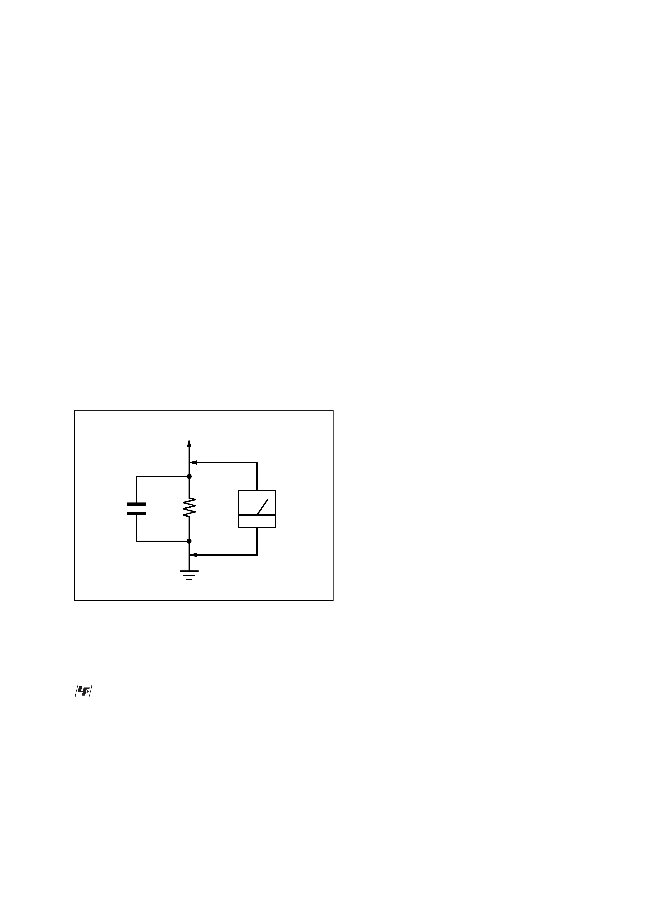
Fig. A.
Using an AC voltmeter to check AC leakage.
1.5 k
0.15
µF
AC
voltmeter
(0.75 V)
To Exposed Metal
Parts on Set
Earth Ground
SAFETY CHECK-OUT
After correcting the original service problem, perform the follow-
ing safety check before releasing the set to the customer:
Check the antenna terminals, metal trim, "metallized" knobs,
screws, and all other exposed metal parts for AC leakage.
Check leakage as described below.
LEAKAGE TEST
The AC leakage from any exposed metal part to earth ground and
from all exposed metal parts to any exposed metal part having a
return to chassis, must not exceed 0.5 mA (500 microamperes.).
Leakage current can be measured by any one of three methods.
1. A commercial leakage tester, such as the Simpson 229 or RCA
WT-540A. Follow the manufacturers' instructions to use these
instruments.
2. A battery-operated AC milliammeter. The Data Precision 245
digital multimeter is suitable for this job.
3. Measuring the voltage drop across a resistor by means of a VOM
or battery-operated AC voltmeter. The "limit" indication is 0.75
V, so analog meters must have an accurate low-voltage scale.
The Simpson 250 and Sanwa SH-63Trd are examples of a pas-
sive VOM that is suitable. Nearly all battery operated digital
multimeters that have a 2 V AC range are suitable. (See Fig. A)
UNLEADED SOLDER
Boards requiring use of unleaded solder are printed with the lead-
free mark (LF) indicating the solder contains no lead.
(Caution: Some printed circuit boards may not come printed with
the lead free mark due to their particular size)
: LEAD FREE MARK
Unleaded solder has the following characteristics.
· Unleaded solder melts at a temperature about 40 °C higher than
ordinary solder.
Ordinary soldering irons can be used but the iron tip has to be
applied to the solder joint for a slightly longer time.
Soldering irons using a temperature regulator should be set to
about 350 °C.
Caution: The printed pattern (copper foil) may peel away if the
heated tip is applied for too long, so be careful!
· Strong viscosity
Unleaded solder is more viscou-s (sticky, less prone to flow)
than ordinary solder so use caution not to let solder bridges oc-
cur such as on IC pins, etc.
· Usable with ordinary solder
It is best to use only unleaded solder but unleaded solder may
also be added to ordinary solder.
TABLE OF CONTENTS
1.
SERVICING NOTES ............................................... 5
2.
GENERAL
Location of Controls .......................................................
9
3.
DISASSEMBLY
3-1. Disassembly Flow ........................................................... 12
3-2. Case (Top)/(Side-L)/(Side-R) ......................................... 13
3-3. Bracket (J)/(P-B) ............................................................. 13
3-4. AMP Board Block ........................................................... 14
3-5. Tuner, COMPONENT/TRIGGER/DVI Board Block .... 14
3-6. S-VIDEO/VIDEO Board Block ..................................... 15
3-7. SUB Board, PREOUT Board, MAIN Board .................. 15
3-8. I. LINK Board, DIGITAL Board .................................... 16
3-9. MOTHER Board Section ................................................ 16
3-10. MOTHER Board ............................................................. 17
4.
TEST MODE .............................................................. 18
5.
ELECTRICAL ADJUSTMENTS ......................... 21
6.
DIAGRAMS
6-1. Block Diagram AUDIO INPUT Section ................. 23
6-2. Block Diagram A/D CONVERTER Section ........... 24
6-3. Block Diagram
DIGITAL INPUT, TUNER Section .......................... 25
6-4. Block Diagram I. LINK Section .............................. 26
6-5. Block Diagram DSP Section ................................... 27
6-6. Block Diagram DIGITAL AUDIO Section ............. 28
6-7. Block Diagram AUDIO OUTPUT Section ............. 29
6-8. Block Diagram POWER AMP Section ................... 30
6-9. Block Diagram VIDEO INPUT/OUT Section ........ 31
6-10. Block Diagram COMPONENT VIDEO Section .... 32
6-11. Block Diagram
DVI, DISPLAY/CONTROL Section ........................ 33
6-12. Block Diagram POWER SUPPLY Section ............. 34
6-13. Note for Printed Wiring Boards
and Schematic Diagrams ................................................ 35
6-14. Printed Wiring Board
DIGITAL Board (Component Side) ......................... 36
6-15. Printed Wiring Board
DIGITAL Board (Conductor Side) ........................... 37
6-16. Schematic Diagram DIGITAL Board (1/11) ........... 38
6-17. Schematic Diagram DIGITAL Board (2/11) ........... 39
6-18. Schematic Diagram DIGITAL Board (3/11) ........... 40
6-19. Schematic Diagram DIGITAL Board (4/11) ........... 41
6-20. Schematic Diagram DIGITAL Board (5/11) ........... 42
6-21. Schematic Diagram DIGITAL Board (6/11) ........... 43
6-22. Schematic Diagram DIGITAL Board (7/11) ........... 44
6-23. Schematic Diagram DIGITAL Board (8/11) ........... 45
6-24. Schematic Diagram DIGITAL Board (9/11) ........... 46
6-25. Schematic Diagram DIGITAL Board (10/11) ......... 47
6-26. Schematic Diagram DIGITAL Board (11/11) ......... 48
6-27. Schematic Diagram MAIN Board (1/3) .................. 49
6-28. Schematic Diagram MAIN Board (2/3) .................. 50
6-29. Schematic Diagram MAIN Board (3/3) .................. 51
6-30. Printed Wiring Board
MAIN Board (Component Side) .............................. 52
6-31. Printed Wiring Board
MAIN Board (Conductor Side) ................................ 53
6-32. Printed Wiring Board
SUB Board (Component Side) ................................. 54
6-33. Printed Wiring Board
SUB Board (Conductor Side) ................................... 55

4
STR-DA9000ES
7.
EXPLODED VIEWS
7-1. Case Section ................................................................... 146
7-2. Disp Board Section ........................................................ 147
7-3. Volume Section .............................................................. 148
7-4. Panel (Door) Section ...................................................... 149
7-5. Front Panel Section ........................................................ 150
7-6. Base Panel Section ......................................................... 151
7-7. AMP Board Section ....................................................... 152
7-8. Tuner Section ................................................................. 153
7-9. Main Board Section ....................................................... 154
7-10. Digital/I. link Board Section .......................................... 155
7-11. Back Panel Section ......................................................... 156
7-12. Transformer Section ....................................................... 157
7-13. MOTHER Board Section ............................................... 158
8.
ELECTRICAL PARTS LIST .............................. 159
6-34. Schematic Diagram SUB Board (1/2) ..................... 56
6-35. Schematic Diagram SUB Board (2/2) ..................... 57
6-36. Printed Wiring Board PREOUT Board ................... 58
6-37. Schematic Diagram PREOUT Board ...................... 59
6-38. Printed Wiring Board VIDEO Board ....................... 60
6-39. Schematic Diagram VIDEO Board ......................... 61
6-40. Printed Wiring Board S-VIDEO Board ................... 62
6-41. Schematic Diagram S-VIDEO Board ...................... 63
6-42. Printed Wiring Board
COMPONENT Section (Component Side) .............. 64
6-43. Printed Wiring Boards
COMPONENT Section (Conductor Side) ............... 65
6-44. Schematic Diagram
COMPONENT Section (1/4) .................................... 66
6-45. Schematic Diagram
COMPONENT Section (2/4) .................................... 67
6-46. Schematic Diagram
COMPONENT Section (3/4) .................................... 68
6-47. Schematic Diagram
COMPONENT Section (4/4) .................................... 69
6-48. Printed Wiring Board TRIGGER Board ................. 70
6-49. Schematic Diagram TRIGGER Board .................... 71
6-50. Schematic Diagram DVI Board (1/2) ...................... 72
6-51. Schematic Diagram DVI Board (2/2) ...................... 73
6-52. Printed Wiring Board DVI Board ............................ 74
6-53. Schematic Diagram AMP Board (1/5) .................... 75
6-54. Schematic Diagram AMP Board (2/5) .................... 76
6-55. Schematic Diagram AMP Board (3/5) .................... 77
6-56. Schematic Diagram AMP Board (4/5) .................... 78
6-57. Schematic Diagram AMP Board (5/5) .................... 79
6-58. Printed Wiring Board
AMP Board (Component Side) ................................. 80
6-59. Printed Wiring Board
AMP Board (Conductor Side) .................................. 81
6-60. Printed Wiring Board FCOIL Board ....................... 82
6-61. Schematic Diagram FCOIL Board .......................... 83
6-62. Printed Wiring Board RCOIL Board ....................... 84
6-63. Schematic Diagram RCOIL Board .......................... 85
6-64. Printed Wiring Boards SP Section ........................... 86
6-65. Schematic Diagram SP Section ............................... 87
6-66. Printed Wiring Board
I. LINK Board (Component Side) ............................ 88
6-67. Printed Wiring Board
I. LINK Board (Conductor Side) .............................. 89
6-68. Schematic Diagram I. LINK Board (1/4) ................ 90
6-69. Schematic Diagram I. LINK Board (2/4) ................ 91
6-70. Schematic Diagram I. LINK Board (3/4) ................ 92
6-71. Schematic Diagram I. LINK Board (4/4) ................ 93
6-72. Printed Wiring Board DISPLAY Section ................ 94
6-73. Schematic Diagram DISPLAY Section ................... 95
6-74. Printed Wiring Boards PANEL Section .................. 96
6-75. Schematic Diagram PANEL Section ....................... 97
6-76. Printed Wiring Board
MOTHER Board (Component Side) ........................ 98
6-77. Printed Wiring Board
MOTHER Board (Conductor Side) .......................... 99
6-78. Schematic Diagram MOTHER Board (1/3) ........... 100
6-79. Schematic Diagram MOTHER Board (2/3) ........... 101
6-80. Schematic Diagram MOTHER Board (3/3) ........... 102
6-81. Schematic Diagram DC Board ............................... 103
6-82. Printed Wiring Board
DC Board (Component Side) .................................. 104
6-83. Printed Wiring Board
DC Board (Conductor Side) .................................... 105
6-84. Printed Wiring Board AC Board ............................. 106
6-85. Schematic Diagram AC Board ................................ 107
6-86. IC Pin Function Description .......................................... 124
5
STR-DA9000ES
SECTION 1
SERVICING NOTES
NOTES ON REPLACEMENT OF I. LINK BOARD
New part of microcomputer (IC3002) and EEPROM (IC3001) on the I. LINK board cannot be used. Therefore, if the mounted I. LINK
board (A-4733-759-A) is replaced, exchange new microcomputer and new EEPROM with that used before the replacement.
OPERATION CHECK OF STANDING BOARDS ON THE MOTHER BOARD
The standing boards connected to the MOTHER board via the connectors can be operated using the jig with the standing boards discon-
nected from the MOTHER board.
In such a case, for the board with the bracket (back panel), remove the board together with the bracket from the MOTHER board, and
connect the bracket to the chassis using a cable attached with alligator clips for GND connection.
Board
Ref. No. of connector
Pitch/Pin
Part No. of jig
Each board
MOTHER board
DIGITAL board
CN2001
CNS801
1.25mm/20 pin
J-2501-260-A
CN2002
CNS802
1.25mm/20 pin
J-2501-260-A
CN2003
CNS803
1.25mm/16 pin
J-2501-258-A
CN2004
CNS804
1.25mm/18 pin
J-2501-259-A
CN2005
CNS805
1.25mm/20 pin
J-2501-260-A
I. LINK board
CN3501
CNS806
1.25mm/16 pin
J-2501-258-A
CN3502
CNS807
1.25mm/18 pin
J-2501-259-A
CN3503
CNS808
1.25mm/6 pin
J-2501-253-A
MAIN board
CN101
CNS810
1.25mm/14 pin
J-2501-257-A
CN102
CNS811
1.25mm/14 pin
J-2501-257-A
CN103
CNS809
1.25mm/8 pin
J-2501-254-A
CN104
CNS825
1.25mm/20 pin
J-2501-260-A
CN105
CNS824
1.25mm/10 pin
J-2501-255-A
PREOUT board
CN1201
CNS822
1.25mm/16 pin
J-2501-258-A
CN1203
CNS823
1.25mm/10 pin
J-2501-255-A
SUB board
CN1003
CNS812
1.25mm/14 pin
J-2501-257-A
CN1002
CNS813
1.25mm/14 pin
J-2501-257-A
CN1001
CNS814
1.25mm/8 pin
J-2501-254-A
CN1006
CNS826
1.25mm/12 pin
J-2501-256-A
VIDEO board
CN302
CNS816
1.25mm/18 pin
J-2501-259-A
CN301
CNS815
1.25mm/8 pin
J-2501-254-A
S-VIDEO board
CN402
CNS817
1.25mm/20 pin
J-2501-260-A
CN401
CNS818
1.25mm/6 pin
J-2501-253-A
COMPONENT board
CN1303
CNS819
1.25mm/20 pin
J-2501-260-A
CN1302
CNS820
1.25mm/16 pin
J-2501-258-A
CN1301
CNS821
1.25mm/20 pin
J-2501-260-A
AMP board
CN1501
CN824
2.5mm/20 pin
J-2501-262-A
CN1507
CN816
2.5mm/6 pin
J-2501-261-A
CN1508
CN815
2.5mm/6 pin
J-2501-261-A
Example of Connection
connecting jig
connecting jig
connecting jig
connecting jig
aligator clip
board