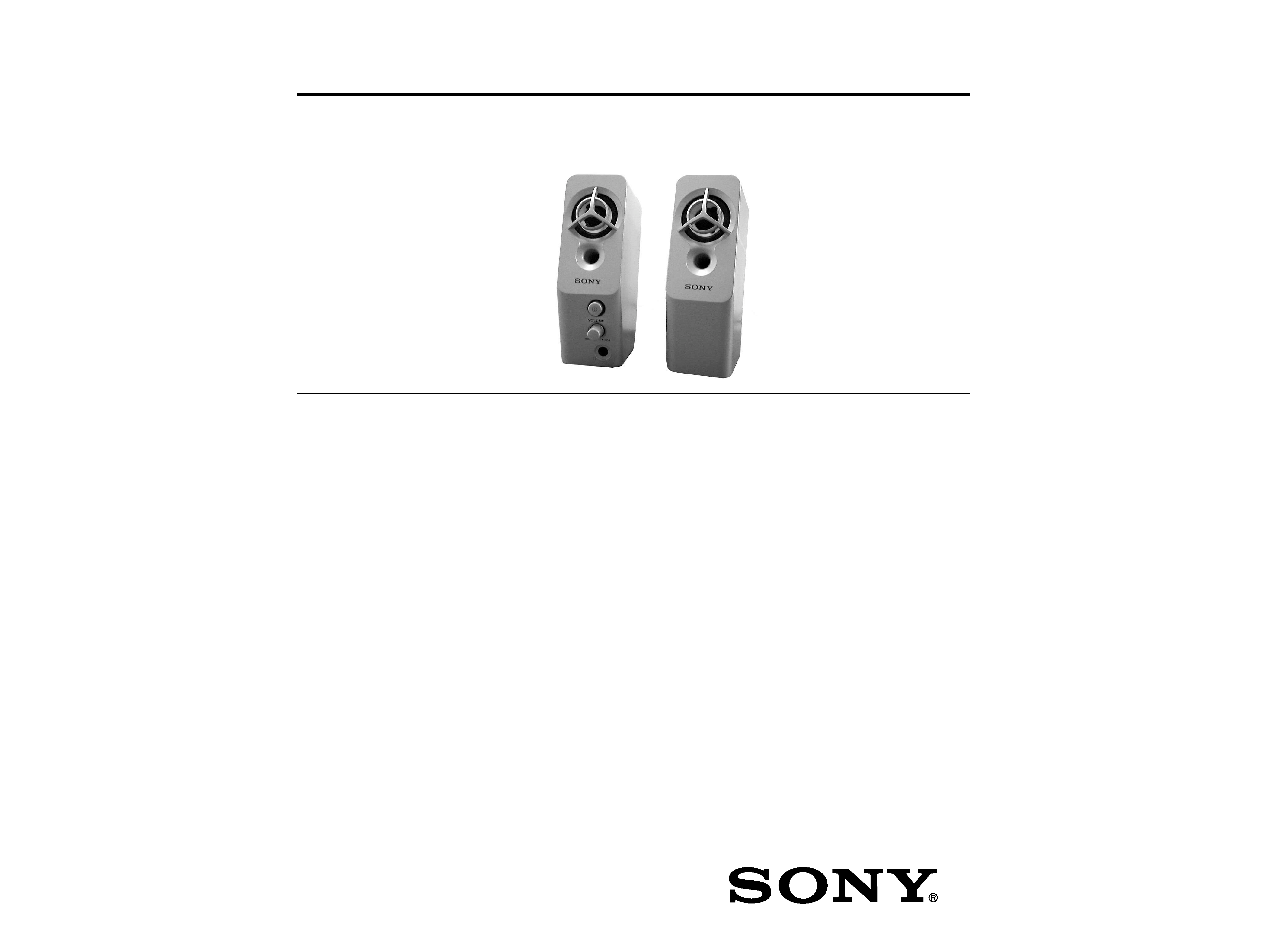
SRS-Z30
SERVICE MANUAL
Ver 1.2 2003.12
US Model
Canadian Model
AEP Model
UK Model
E Model
Australian Model
Tourist Model
9-877-075-03
2003L02-1
© 2003.12
Sony Corporation
Personal Audio Company
Pubulished by Sony Engineering Corporation
ACTIVE SPEAKER SYSTEM
Speaker section
Enclosure type
Full range, Bass reflex,
magnetically shielded
Speaker system
39 mm (diameter)
Impedance
8
Rated input power
3 W
Amplifier section (Left Speaker)
Rated output
3 W + 3 W (10 % T.H.D., 1 kHz, 6
)
Bass boost
MEGA BASS
Input Input cord a stereo-mini plug (2 m) x 1
Stereo mini jack x 1
Input impedance
4.7 k
(at 1 kHz)
Output
Stereo mini jack x 1 (PHONES)
General
Power
DC 9V (supplied AC power adaptor)
Dimensions (w/h/d)
approx. 50 x 145 x 70 mm
(2 x 5 3/4 x 2 7/8 inch)
Mass
(Left) 250 g (9 oz.),(Right) 200 g (7 oz.)
Supplied accessories
AC power adaptor (1)
Operating Instructions (1)
Design and specifications are subject to change without notice.
SPECIFICATIONS
2
Specifications ............................................................................ 1
1. GENERAL
Locating the Controls ......................................................... 2
2. DIAGRAMS
2-1. Schematic Diagram ..................................................... 3
2-2. Printed Wiring Boards (1/2) ....................................... 4
2-3. Printed Wiring Boards (2/2) ....................................... 5
3. EXPLODED VIEWS
3-1. Main Section ............................................................... 7
4. ELECTRICAL PARTS LIST ..................................... 8
SAFETY-RELATED COMPONENT WARNING!!
COMPONENTS IDENTIFIED BY MARK 0 OR DOTTED LINE
WITH MARK 0 ON THE SCHEMATIC DIAGRAMS AND IN THE
PARTS LIST ARE CRITICAL TO SAFE OPERATION.
REPLACE THESE COMPONENTS WITH SONY PARTS WHOSE
PART NUMBERS APPEAR AS SHOWN IN THIS MANUAL OR IN
SUPPLEMENTS PUBLISHED BY SONY.
Notes on chip component replacement
· Never reuse a disconnected chip component.
· Notice that the minus side of a tantalum capacitor may be dam-
aged by heat.
TABLE OF CONTENTS
CAUTION
Use of controls or adjustments or performance of procedures other
than those specified herein may result in hazardous radiation
exposure.
SRS-Z30
z
UNLEADED SOLDER
Boards requiring use of unleaded solder are printed with the
lead-free mark (LF) indicating the solder contains no lead.
(Caution: Some printed circuit boards may not come printed
with the lead free mark due to their particular size.)
: LEAD FREE MARK
Unleaded solder has the following characteristics.
· Unleaded solder melts at a temperature about 40
°C higher
than ordinary solder.
Ordinary soldering irons can be used but the iron tip has to
be applied to the solder joint for a slightly longer time.
Soldering irons using a temperature regulator should be set
to about 350
°C.
Caution: The printed pattern (copper foil) may peel away if
the heated tip is applied for too long, so be careful!
· Strong viscosity
Unleaded solder is more viscous (sticky, less prone to
flow) than ordinary solder so use caution not to let solder
bridges occur such as on IC pins, etc.
· Usable with ordinary solder
It is best to use only unleaded solder but unleaded solder
may also be added to ordinary solder.
ATTENTION AU COMPOSANT AYANT RAPPORT
À LA SÉCURITÉ!
LES COMPOSANTS IDENTIFÉS PAR UNE MARQUE 0 SUR
LES DIAGRAMMES SCHÉMATIQUES ET LA LISTE DES
PIÈCES SONT CRITIQUES POUR LA SÉCURITÉ DE
FONCTIONNEMENT. NE REMPLACER CES COMPOSANTS
QUE PAR DES PIÈSES SONY DONT LES NUMÉROS SONT
DONNÉS DANS CE MANUEL OU DANS LES SUPPÉMENTS
PUBLIÉS PAR SONY.
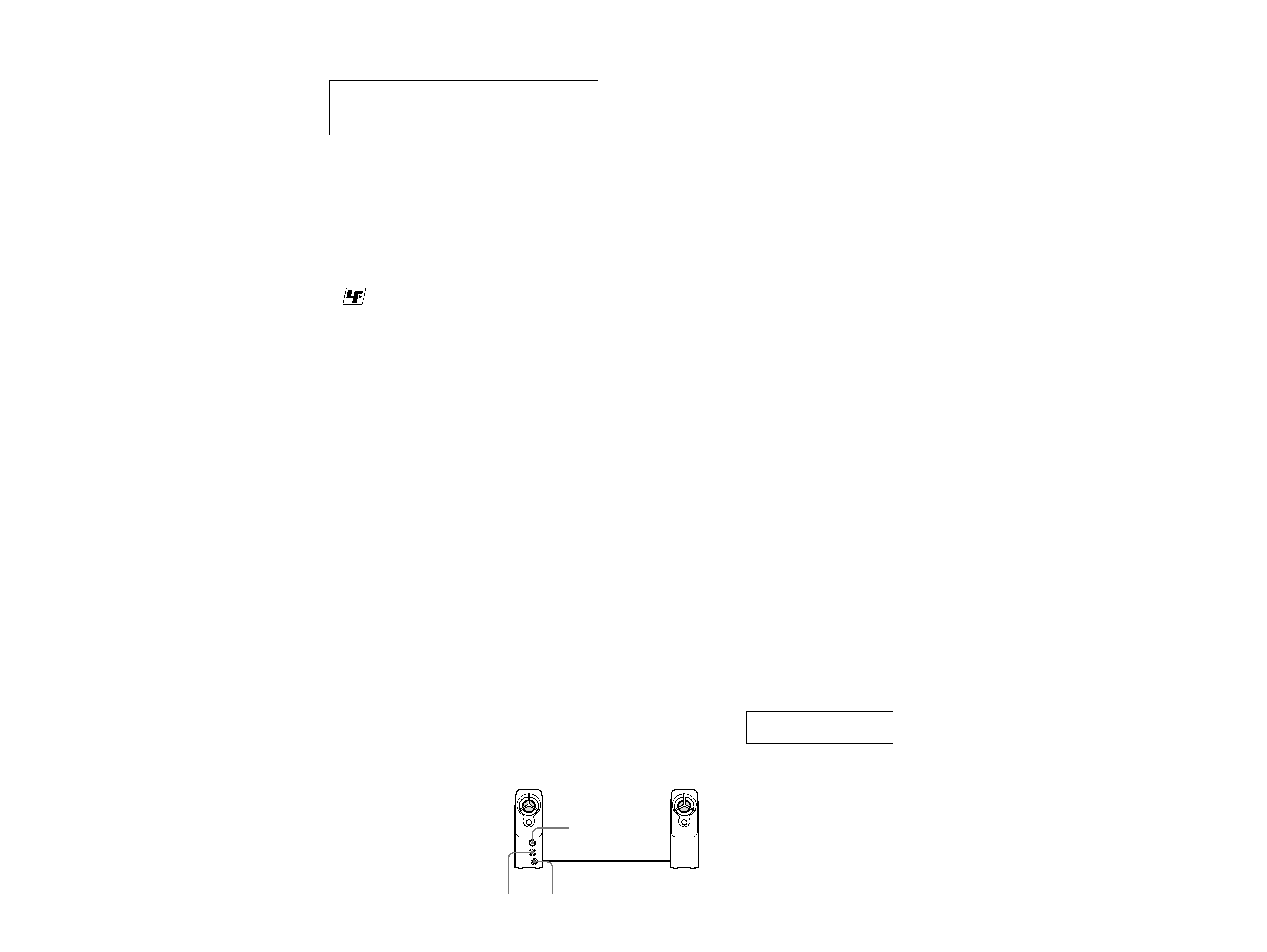
SECTION 1
GENERAL
Left speaker (front)
Right speaker (front)
POWER
VOLUME
PHONES
This section is extracted from
instruction manual.
LOCATING THE CONTROLS
33
SRS-Z30
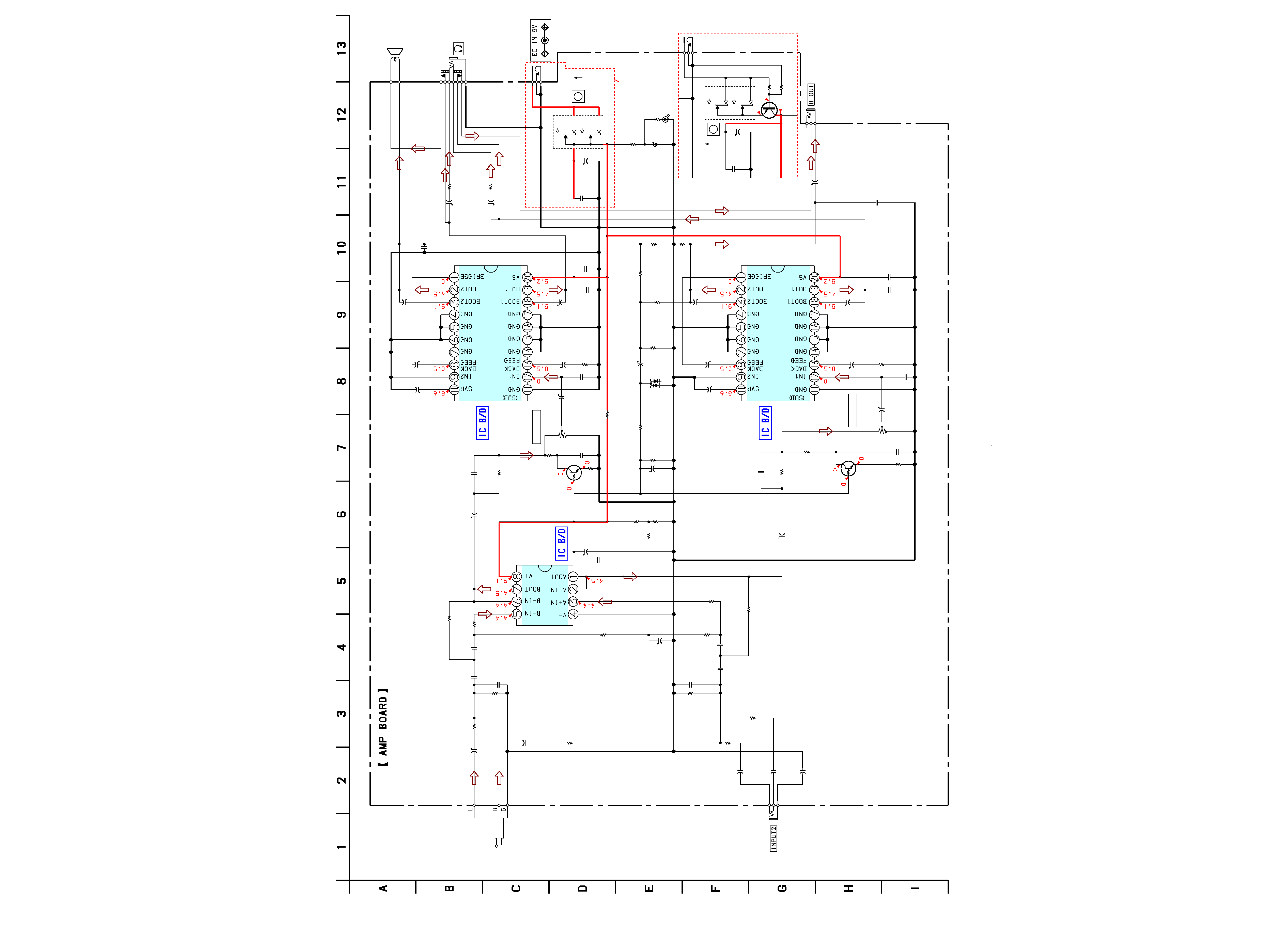
SECTION 2
DIAGRAMS
2-1. SCHEMATIC DIAGRAM
· Refer to page 6 for Notes.
R31
D3
C6
C4
R2
C13
C15
R11
R39
C55
C106
R7
R10
C19
C20
C27
R35
R33
R32
R14
R17
R20
R15
C22
C25
RV1(2/2)
C28
C108
C37
R24
C41
C44
C46
R30
C50
C49
R29
C48
C42
C38
C34
IC2
IC3
R4
R1
R3
R5
C14
C16
C105
R9
R38
R12
C54
C24
R16
R21
RV1(1/2)
R19
C26
C29
C107
R23
C35
C39
C43
C45
C52
D4
C53
C51
R28
R27
R26
R25
R34
C30
D1
R18
R22
C23
C32
C36
C40
C47
JK2
JK3
CL4
CL5
P1
CL1
CL2
CL3
SP1
JK4
JK1
S1
C8
C9
C10
IC1
Q1
Q2
R40
LED
LT0323-41-URF4
10
16V
10
16V
3.3k
0.047
0.047
12k
470
1
50V
100p
2.7k
180k
0.1
47
16V
10
16V
180k
10k
10k
91
220
3.3k
4.7k
4700
0.1
5K
1
50V
100p
100
4V
91
100
16V
1
0.1
91
100
4V
100
4V
91
1
100
16V
100
4V
100
16V
TEA2025D
POWER AMP
(L-CH)
TEA2025D
POWER AMP
(R-CH)
3.3k
3.3k
3.3k
2.7k
0.047
0.047
100p
180k
470
12k
1
50V
4700
4.7k
3.3k
5K
220
0.1
1
50V
100p
91
100
4V
100
16V
1
0.1
1000
6.3V
UDZ6.8B
1000
16V
0.1
470
470
1k
1k
1k
10
16V
1SS226
10k
10k
47
4V
100
16V
100
4V
100
16V
1
(INPUT1)
10
16V
BP
10
16V
BP
10
16V
BP
LM358D
PRE AMP
DTC144TKA
MEGA BASS
DTC144TKA
MEGA BASS
91
180
VOLUME
VOLUME
SPEAKER
-
S1
-2
-1
OFF
ON
EXCEPT JEW
C53
C51
JK4
R37 2.2k
R36
8.2k
S1
Q3
2SB1436
B+ SWITCH
1000
16V
0.1
-
S1
-2
-1
OFF
ON
JEW
9.2
9.2
8.6
Ver 1.2
4
4
SRS-Z30
IC3
Q2
IC2
IC1
Q1
D1
C8
C9
C13
C14
C15
C16
C19
C20
C22
C24
C25
C26
C32
C34
C35
C36
Q3
C37
C38
C39
C40
C41
C42
C43
C44
C45
C46
C49
C50
C47
C48
C51
C105 C106
C107
C108
C53
C52
C10
C28
C29
C23
C30
C54
C55
C27
C4
C6
R2
R36
R37
JEW
R3
R1
R29
R5 R7
R12
R9
R38
R30
R14
R11
R35
R10
R39
R33
R32
R15
R16
R31
R40
R19
R22
R18
R21
R20
R17
R34
R26
E
JEW
C
B
R25
R28
R27
R24
R23
R4
E
E
1
1
10
10
11
11
20
20
L+
L
SP1
SPEAKER
AMP BOARD (SIDE A)
12
(12)
1-685-794-
D4
2
3
4
5
6
A
1
B
C
2-2. PRINTED WIRING BOARDS (1/2) · Refer to page 6 for Notes.
· Semiconductor
Ref. No.
Location
D1
B-4
IC1
B-2
IC2
B-5
IC3
A-5
Q1
C-4
Q2
C-4
Q3
B-4
: USES UNLEADED SOLDER.
Ver 1.2
55
SRS-Z30
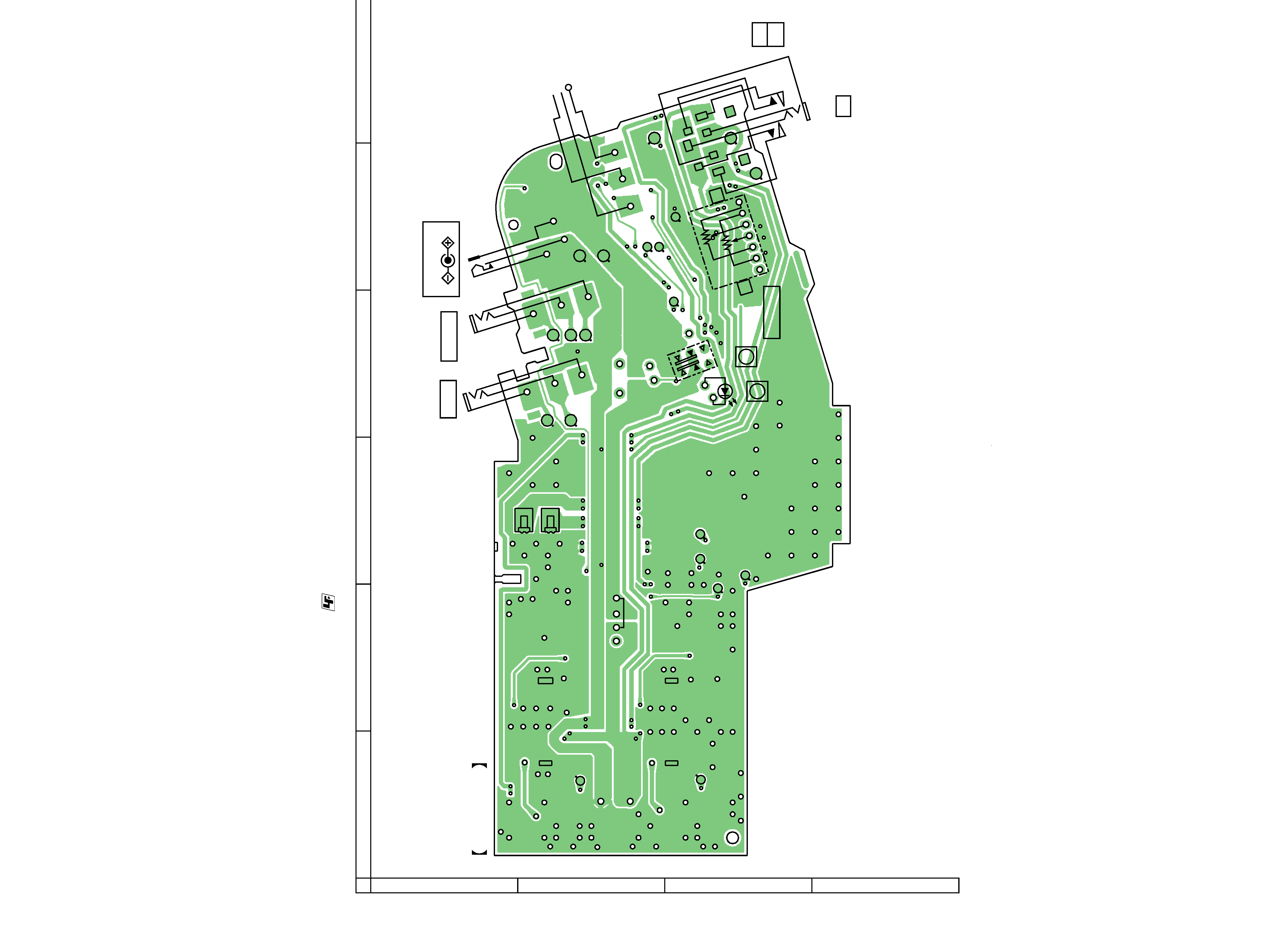
2-3. PRINTED WIRING BOARDS (2/2) · Refer to page 6 for Notes.
: USES UNLEADED SOLDER.
CL1
CL2
CL5
CL4
CL3
TP8
TP23
TP7
TP2
TP19
TP9
TP11
JW1
TP10
TP21
TP22
TP3
TP14
TP13
TP17
TP1
TP12
TP20
TP18
R
G
L
TP15
TP16
12
(12)
1-685-794-
AMP BOARD (SIDE B)
DC IN 9V
JK4
JK2
R OUT
JK1
INPUT 2
P1
(INPUT 1)
RV1
VOLUME
D3
JK3
i
I
S1
ON
r
OFF
I
2
3
4
5
6
A
1
B
C
D