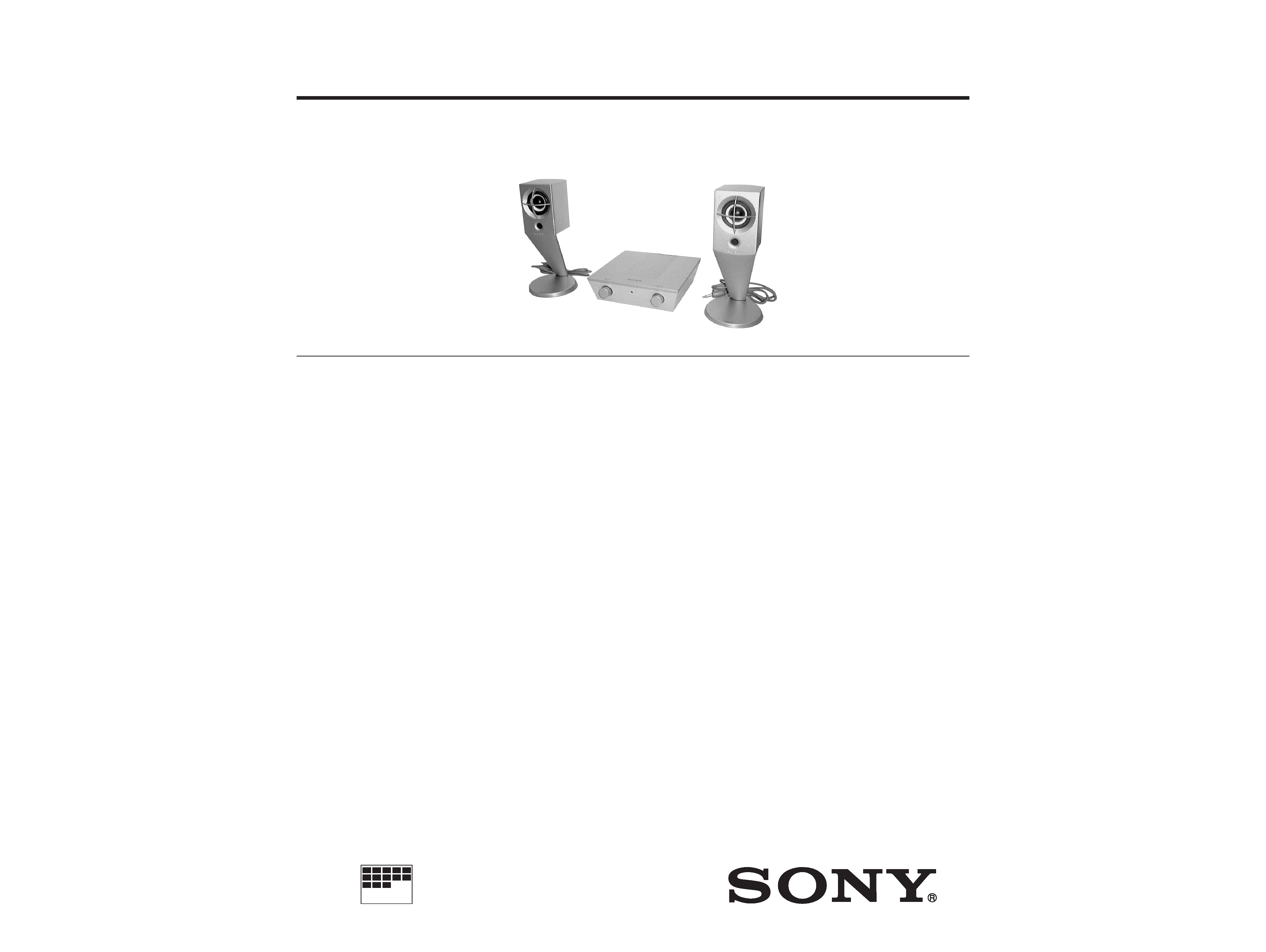
SRS-Z1
US Model
Canadian Model
AEP Model
UK Model
E Model
Australian Model
Tourist Model
SERVICE MANUAL
STEREO ACTIVE SPEAKER SYSTEM
MICROFILM
SPECIFICATIONS
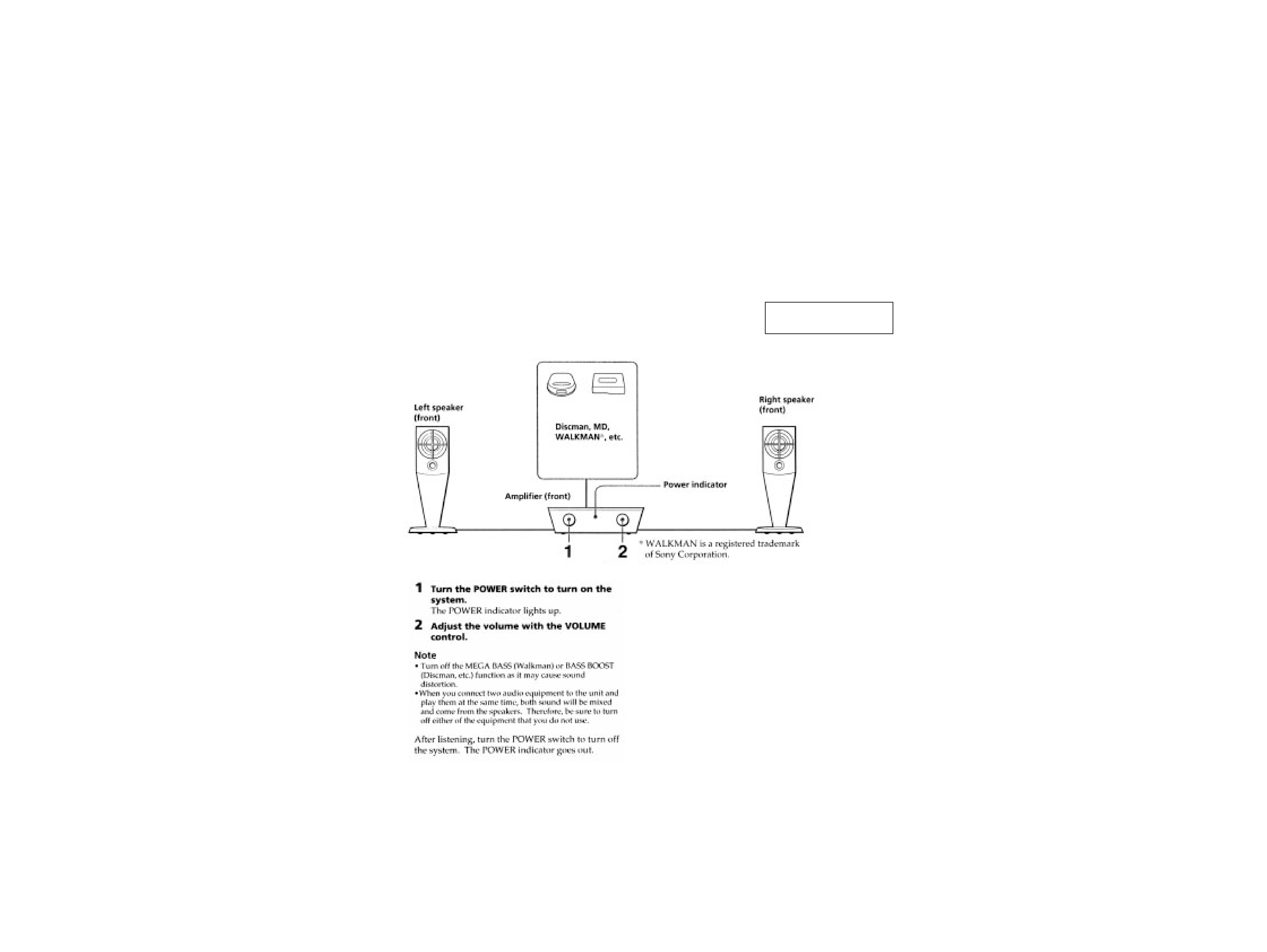
Amplifier
Power output
3 W + 3 W
Input impedance
4.7 k
(at 1 kHz)
Input
Stereo mini jack
× 2 (INPUT1, 2)
Dimensions
Approx. 140
× 40 × 140 mm
(55/8
× 15/8 × 55/8 in.) (w/h/d)
Mass
Approx. 590 g 1lb 5 oz
Speakers
System
Full-range, bass reflex type
Speaker unit
Magnetically shielded ø39 mm
(19/16 inch)
Nominal Impedance 8
Rated input power
3 W
Dimensions
Approx. 80
× 176 × 80 mm
(31/4
× 7 × 31/4 in.) (w/h/d)
Mass
Approx. 380 g 13 oz
General
Power requirement
DC IN 9 V jack accepts the supplied
Sony AC power adaptor
Supplied accessories AC power adaptor (1)
Connecting cord
(stereo miniplug
stereo miniplug) (1)
Design and specifications are subject to change without notice.
REVISED
Ver 1.2 1999. 09
-- 2 --
TABLE OF CONTENTS
1. GENERAL ·········································································· 2
2. DIAGRAMS
2-1.
IC Block Diagram ······························································ 3
2-2.
Printed Wiring Board ·························································· 4
2-3.
Schematic Diagram ···························································· 5
3. EXPLODED VIEWS ··················································· 7
4. ELECTRICAL PARTS LIST ····································· 9
SECTION 1
GENERAL
This section is extracted
from instruction manual.
SAFETY-RELATED COMPONENT WARNING!!
COMPONENTS IDENTIFIED BY MARK
! OR DOTTED LINE WITH
MARK
! ON THE SCHEMATIC DIAGRAMS AND IN THE PARTS
LIST ARE CRITICAL TO SAFE OPERATION. REPLACE THESE
COMPONENTS WITH SONY PARTS WHOSE PART NUMBERS
APPEAR AS SHOWN IN THIS MANUAL OR IN SUPPLEMENTS
PUBLISHED BY SONY.
ATTENTION AU COMPOSANT AYANT RAPPORT
À LA SÉCURITÉ!
LES COMPOSANTS IDENTIFÉS PAR UNE MARQUE
! SUR LES
DIAGRAMMES SCHÉMATIQUES ET LA LISTE DES PIÈCES SONT
CRITIQUES POUR LA SÉCURITÉ DE FONCTIONNEMENT. NE
REMPLACER CES COMPOSANTS QUE PAR DES PIÈSES SONY
DONT LES NUMÉROS SONT DONNÉS DANS CE MANUEL OU
DANS LES SUPPÉMENTS PUBLIÉS PAR SONY.
SECTION 2
DIAGRAMS
2-1. IC BLOCK DIAGRAM
· IC1, IC2 TEA2025B
50
5K
10K
10K
50
50
DECOUPLING
START
CIRCUIT
PROTECT.
THERMAL
9
10
11
12
13
14
15
16
BRIDGE
OUT2
BOOT2
GND
GND
IN2+
SVR
FEED
BACK
+Vs
OUT1
BOOT1
GND
GND
IN1+
GND
FEED
BACK
1
2
3
4
5
6
7
8
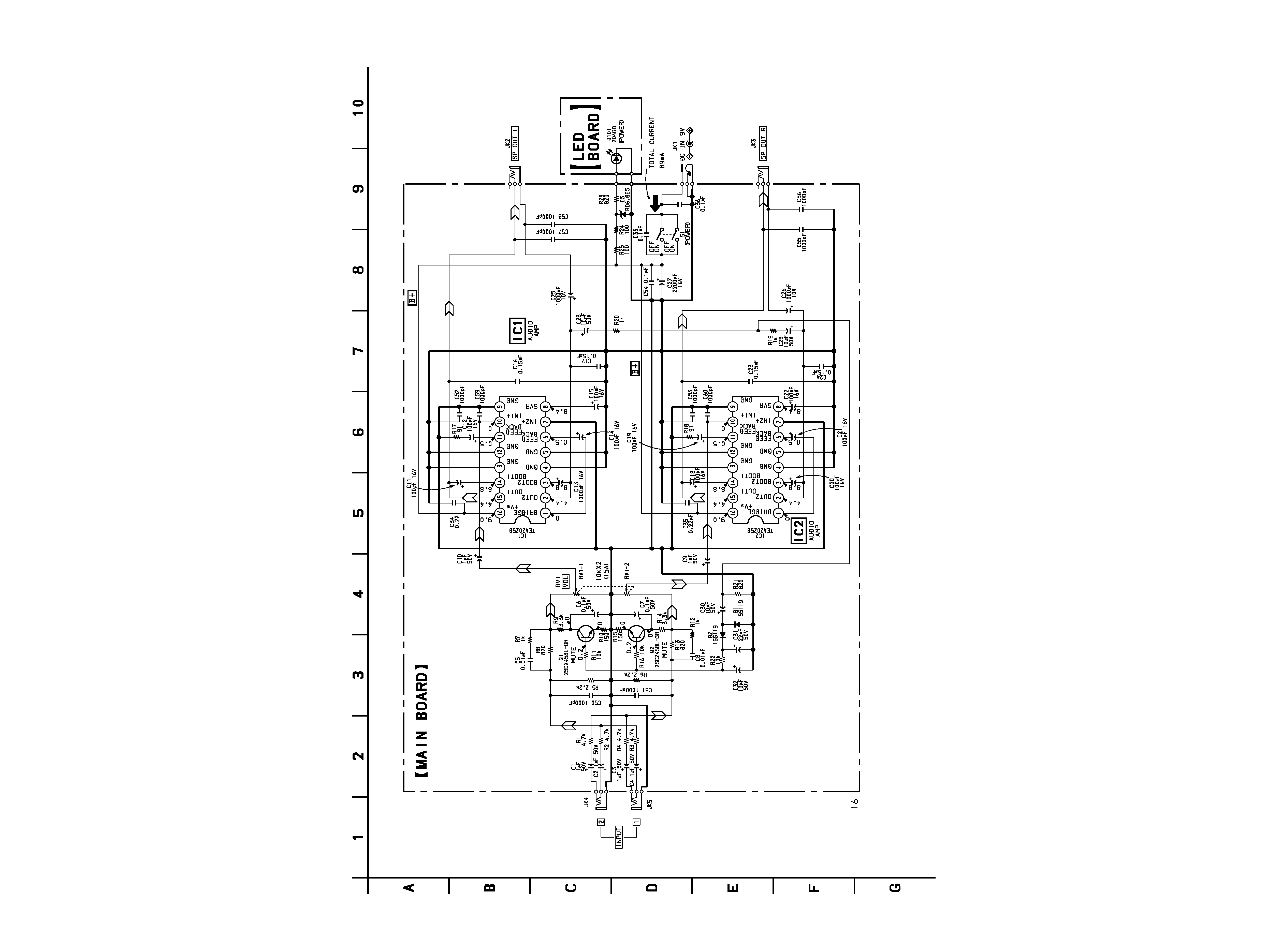
Note on Schematic Diagram:
· All capacitors are in µF unless otherwise noted. pF: µµF
50 WV or less are not indicated except for electrolytics
and tantalums.
· All resistors are in
and 1/4 W or less unless otherwise
specified.
· C : panel designation.
· U : B+ Line.
· Power voltage is dc 9 V and fed with regulated dc power
supply from battery terminal.
· Voltages and waveforms are dc with respect to ground
under no-signal (detuned) conditions.
· Voltages are taken with a VOM (Input impedance 10 M
).
Voltage variations may be noted due to normal produc-
tion tolerances.
· Signal path.
E
: AUDIO signal
Note on Printed Wiring Board:
· X : parts extracted from the component side.
· b : Pattern from the side which enables seeing.
-- 3 --
2-2. PRINTED WIRING BOARD
C4
C50
R4
C3
C27
R8
R9
R2
R3
C2
C1
R5
R6
R12
R14
C51
MAIN BOARD
LED BOARD
C5
C7
C8
C6
C33
C36
R7
R11
R10
R16
R15
R25
R22
R19
R21
R20
R23
R24
R13
R1
B
C
E
B
C
E
Q2
Q1
S1
(POWER)
D101
(POWER)
RED
BLK
C32
C31
D3
D2 D1
C30
C28
C14
C13
C56
C57
C55
C58
C15
C10
C19
C18
C23
C20
C11
C21
C26
C16
C17
C25
C24
IC2
C9
C53
C22
C29
C52
C12
C60
C35
C59
R17
R18
18
9
10
16 15
5
IC1
18
9
10
16 15
5
1-673-371-
1-673-372-
(11)
11
(11)
11
RV1
VOL
JK3
SP OUT R
JK2
SP OUT L
JK1
DC IN 9V
INPUT
(CHASSIS)
JK4
JK5
2
1
-1
-2
12
A
B
C
D
E
F
34567
16
· Refer to page 3 for Note on Printed Wiring Board.
SRS-Z1
Ref. No.
Location
D1
C-5
D2
C-5
D3
C-6
D101
B-7
IC1
D-4
IC2
E-4
Q1
B-4
Q2
C-4
· Semiconductor
Location
-- 4 --
SRS-Z1
-- 5 --
-- 6 --
2-3. SCHEMATIC DIAGRAM
· Refer to page 3 for IC Block Diagram and Note on Schematic Diagram.