Ver 1.0 2001.03
ACTIVE SPEAKER SYSTEM
9-873-102-11
2001C0200-1
© 2001.3
Sony Corporation
Audio Entertainment Group
General Engineering Dept.
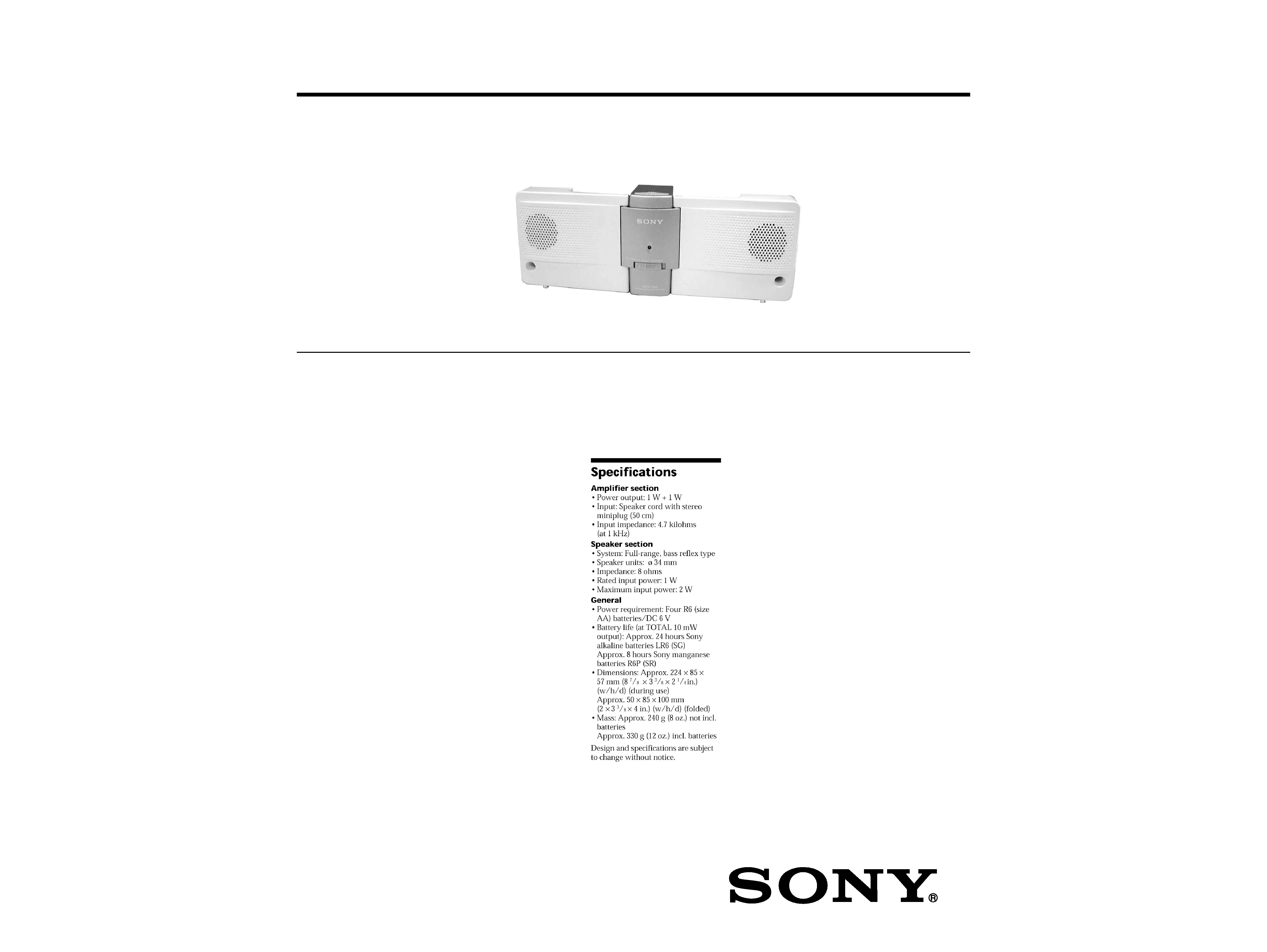
SRS-T55
SERVICE MANUAL
SPECIFICATIONS
E Model
2
SRS-T55
Specifications ........................................................................... 1
1. GENERAL ...................................................................... 2
2. DISASSEMBLY
2-1. Battery box ................................................................. 3
2-2. Speaker ....................................................................... 3
2-3. AMP board, DC Jack board ........................................ 4
3. DIAGRAMS
3-1. Printed Wiring Boards ................................................ 5
3-2. Schematic Diagram ..................................................... 6
6. EXPLODED VIEWS .................................................... 7
7. ELECTRICAL PARTS LIST ..................................... 8
TABLE OF CONTENTS
SECTION 1
GENERAL
This section is extracted from
instruction manual.
Notes on chip component replacement
· Never reuse a disconnected chip component.
· Notice that the minus side of a tantalum capacitor may be dam-
aged by heat.
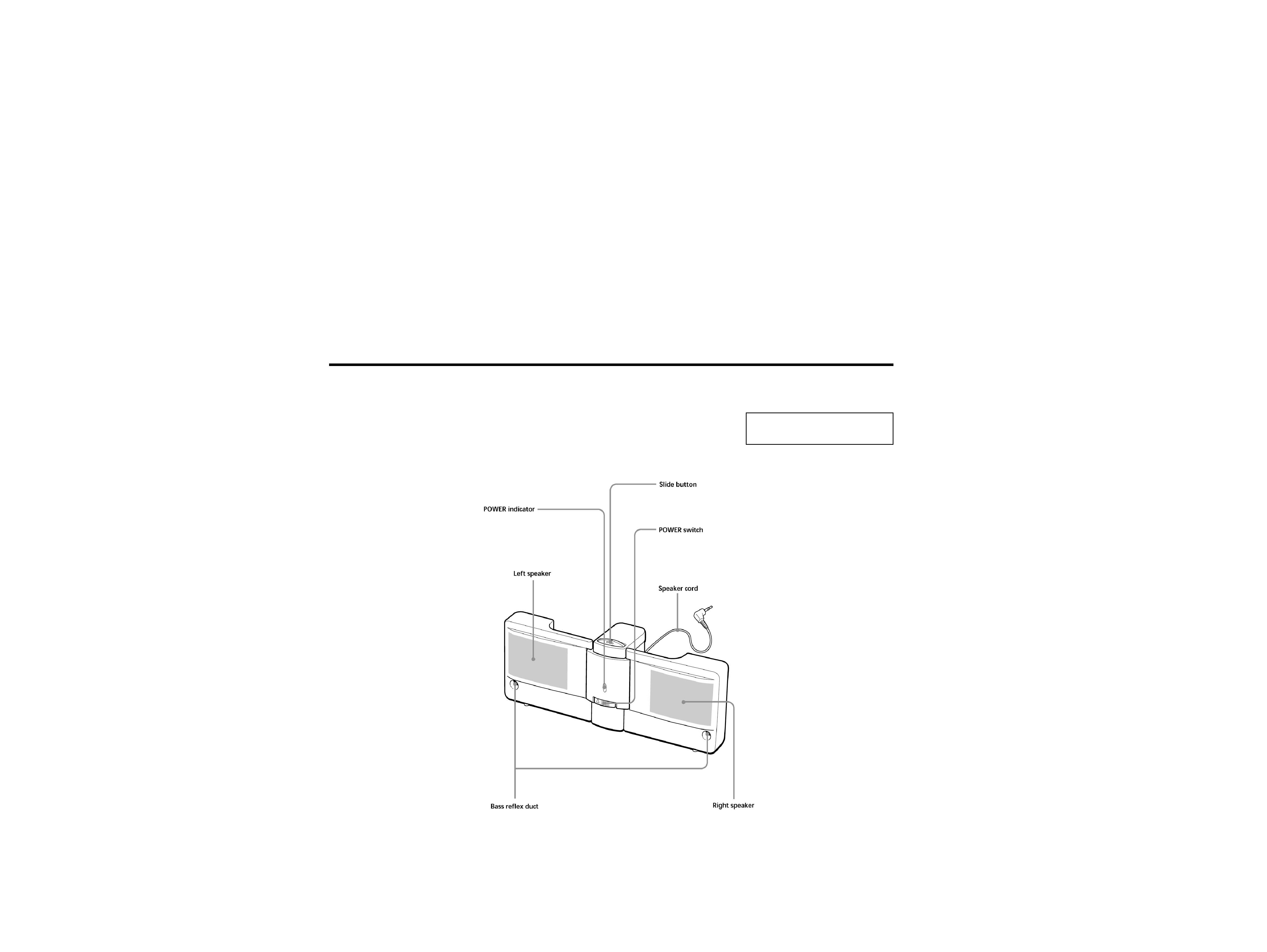
LOCATION AND FUNCTION OF CONTROLS
3
SRS-T55
SECTION 2
DISASSEMBLY
2-1. BATTERY BOX
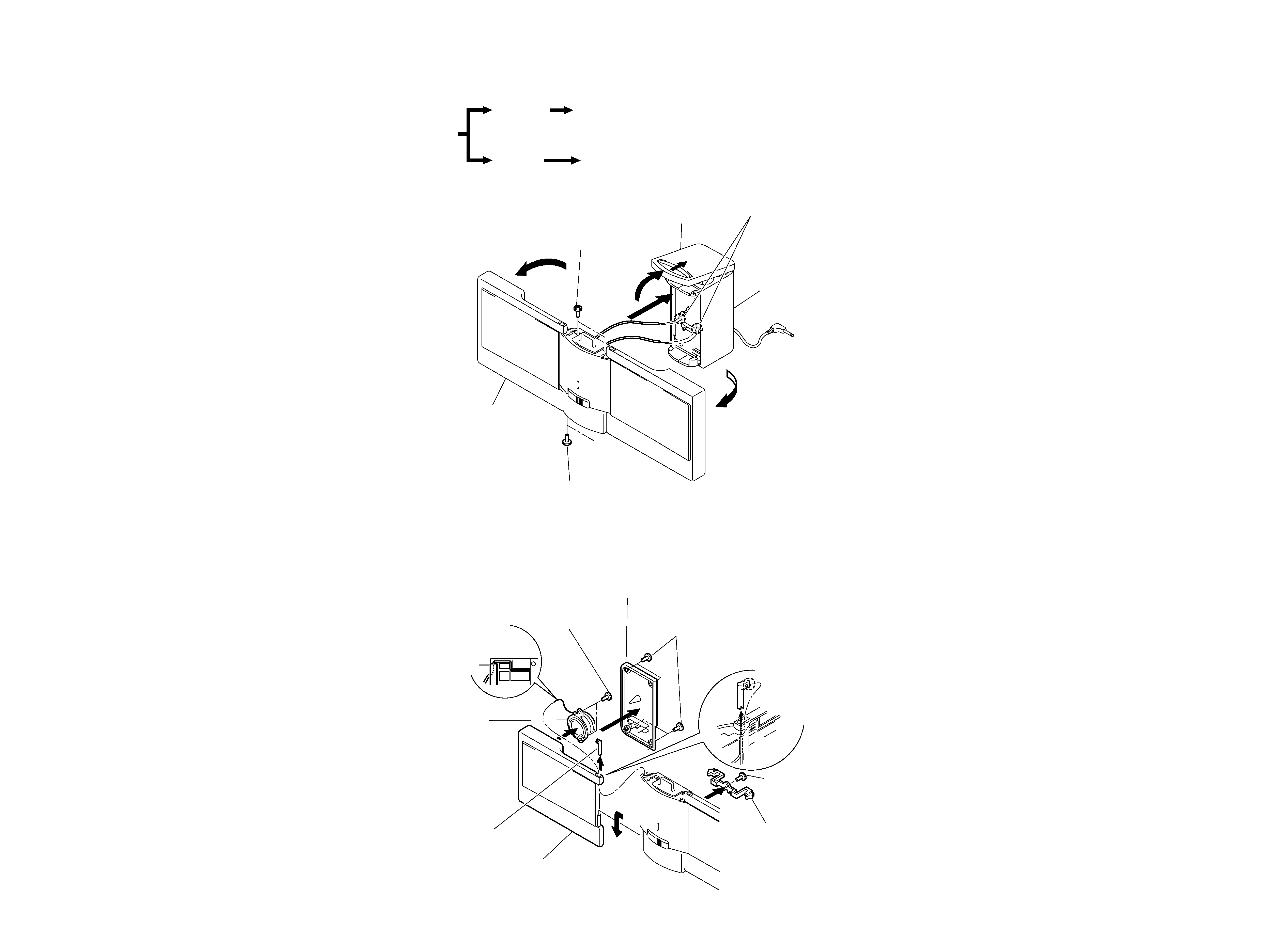
2-2. SPEAKER
· The equipment can be removed using the following procedure.
Note :
Remove Speaker (R) in the same way.
2
6
4
7
B
9
3 Screws (+ P2X6)
8 Screws (+2.6X6)
1 Screws (+ P2X5)
Cabinet (L), rear
Speaker
lead
Cabinet (L), front
Bar, tension
Shaft (L), rotary
Speaker (L)
(SP1)
A
5 Remove the speaker
lead from groove of
"Cabinet (L), front".
On attaching, set it
as shown in the
figure.
While pushing claw in the arrow
A
direction, remove "Shaft (L),
rotary" by pushing it out in the
arrow B direction.
2
4
3
6
1
5 Screws (+ P2X6)
7 Remove soider
(four places)
5 Screws (+ P2X6)
Front section
Battery box
Lid, battery case
Set
Front section
Speaker
Battery box
AMP board, DC Jack board
Note : Follow the disassembly procedure in the numerical order given.
4
SRS-T55
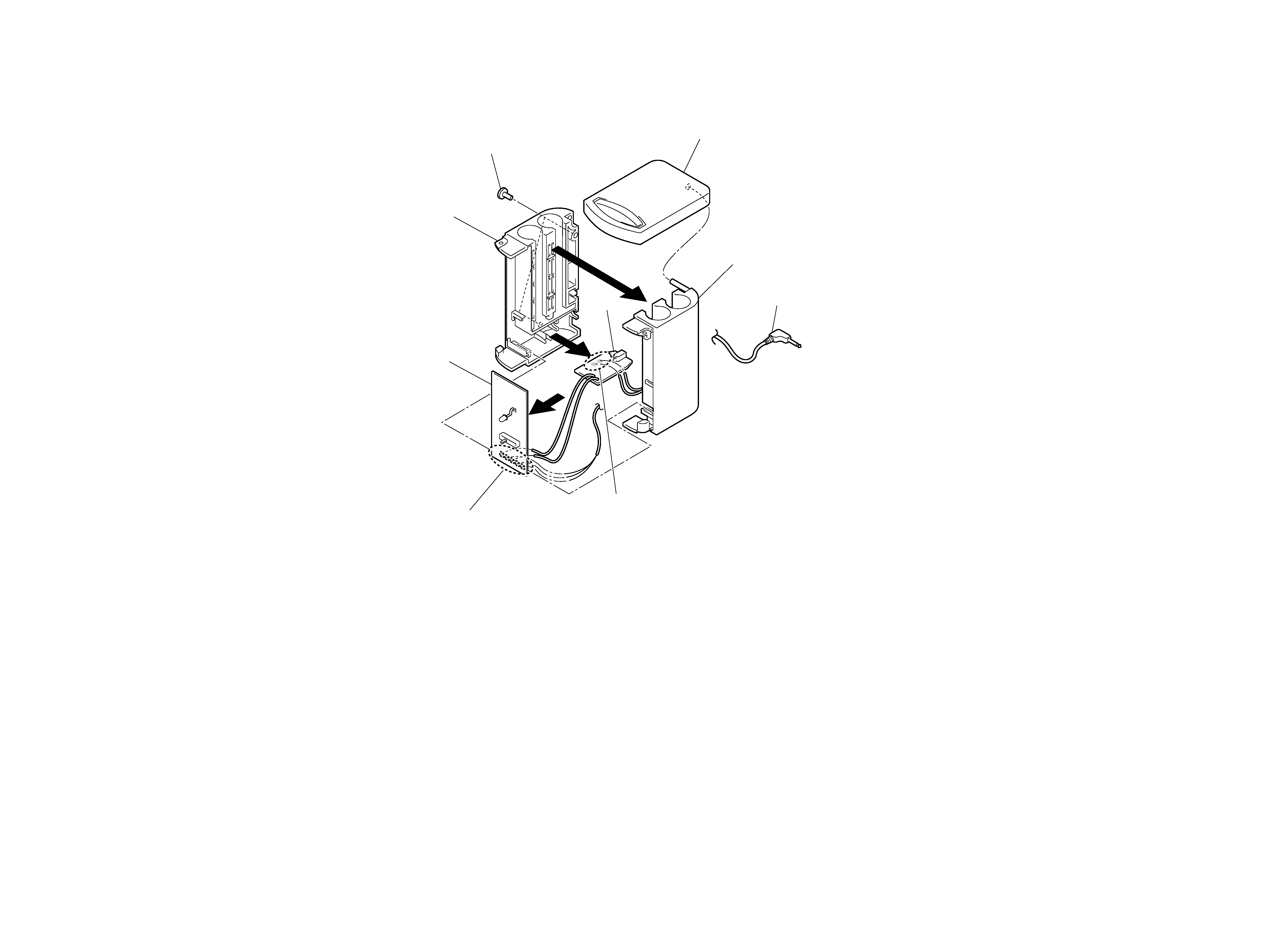
2-3. AMP BOARD, DC JACK BOARD
5
2
3
1 Screws (+ P2X6)
Lid, battery case
Box (L), battery
AMP board
DC Jack board
Box (R), battery
Cord (with plug)
6 Remove solder
(two places)
4 Remove solder
(five places)
5
5
SRS-T55
12
(12)
1-679-480-
12
(12)
1-679-473-
12
(12)
1-679-473-
DC JACK BOARD (SIDE A)
AMP BOARD (SIDE A)
AMP BOARD (SIDE B)
DC JACK BOARD (SIDE B)
12
(12)
1-679-480-
BCE
Q2
BCE
Q1
R11
R9
R1
R5
R7
R3
R15
C21
C19
R16
R17
C20
C1
C103
R6
C25
R20
R18
C18
R10
R12
C2
-1
-3
-4
-2
C104
C101
C26
R4
C102
OFF/DIRECT
C24
R19
R2
V+
V+
GND
GND
R
L
G
R8
R14
C23
D1
D3
C13
C16
C15
C4
C3
C22
C5
C6
C14
C10
C17
+
-
C9
C7
C8
C12
C11
SP2
SPEAKER(R)
8
+
-
SP1
SPEAKER(L)
8
P1
(INPUT)
ON
r
S1
POWER
1
5
11
15
20
10
IC2
1
5
11
15
20
10
IC1
DRY BATTERY
SIZE "AA"
(IEC DESIGNATION LR6)
4PCS, 6V
JK1
DC IN 6V
D2
POWER
2
3
4
5
6
7
8
9
1
B
C
D
E
F
G
A
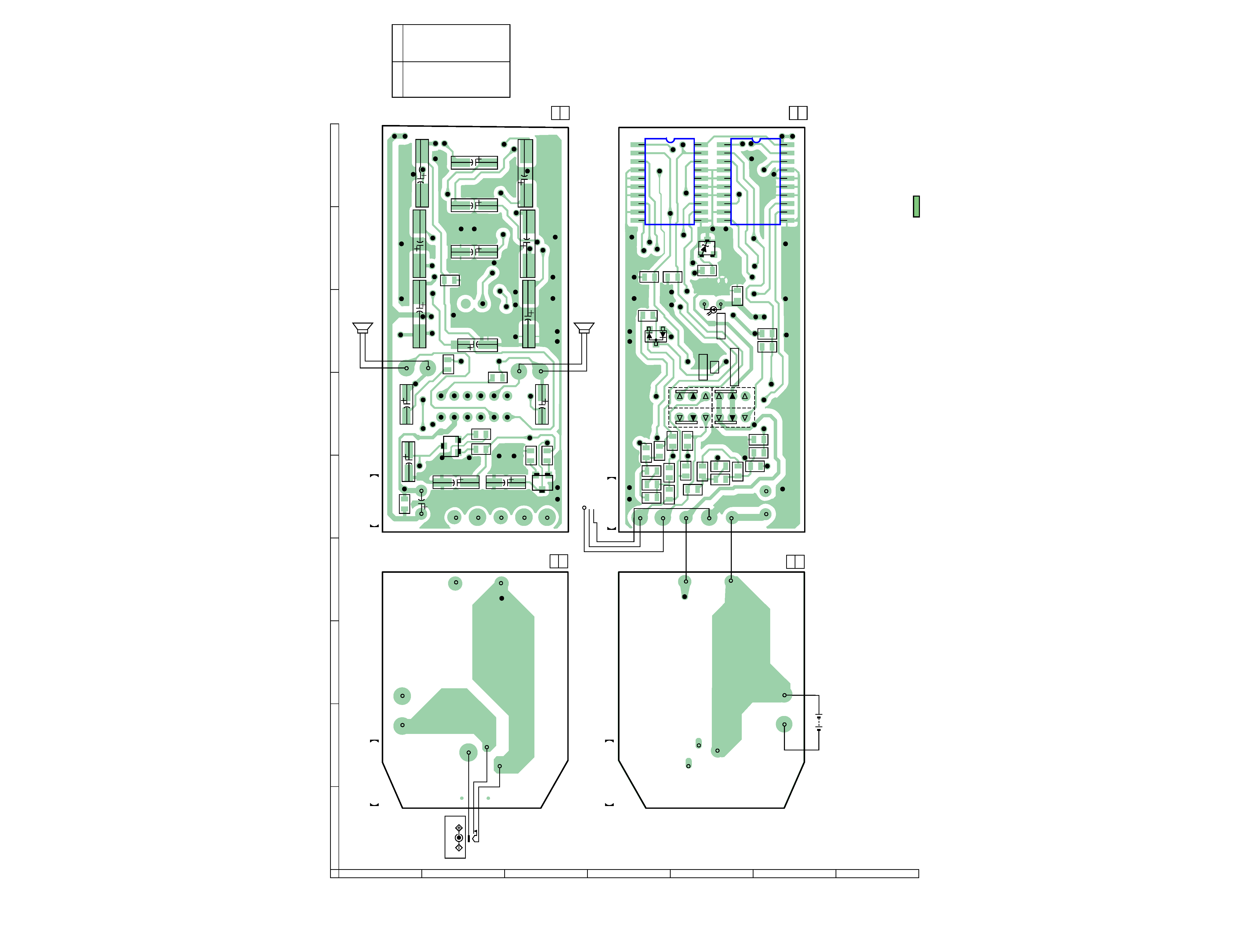
3-1. PRINTED WIRING BOARDS
D1
D-7
D2
E-7
D3
E-8
IC1
F-9
IC2
D-9
Q1
B-6
Q2
C-5
Ref. No.
Location
z
Semiconductor
Location
SECTION 3
DIAGRAMS
Note:
· X : parts extracted from the component side.
·
z
: Through hole.
·
: Pattern from the side which enables seeing.
(The other layers' patterns are not indicated.)