Ver 1.0 2000.01
MICROFILM
SRS-A37/A47
SERVICE MANUAL
ACTIVE SPEAKER SYSTEM
SPECIFICATIONS
US Model
Canadian Model
SRS-A37
AEP Model
E Model
SRS-A37/A47
UK Model
Australian Model
SRS-A47
Photo : SRS-A37
Amplifier section
Power output
1.5W + 1.5W (SRS-A37)
2.0W + 2.0W (SRS-A47)
Input impedance
4.7 kiloohms (at 1kHz)
Speaker section
System
Full-range, bass reflex type
Speaker unit
Full-range (magnetically shielded):
57mm (2 1/
4
in.)
Nominal impedance
8 ohms
Rated input power
1.5W (SRS-A37)
2W (SRS-A47)
General
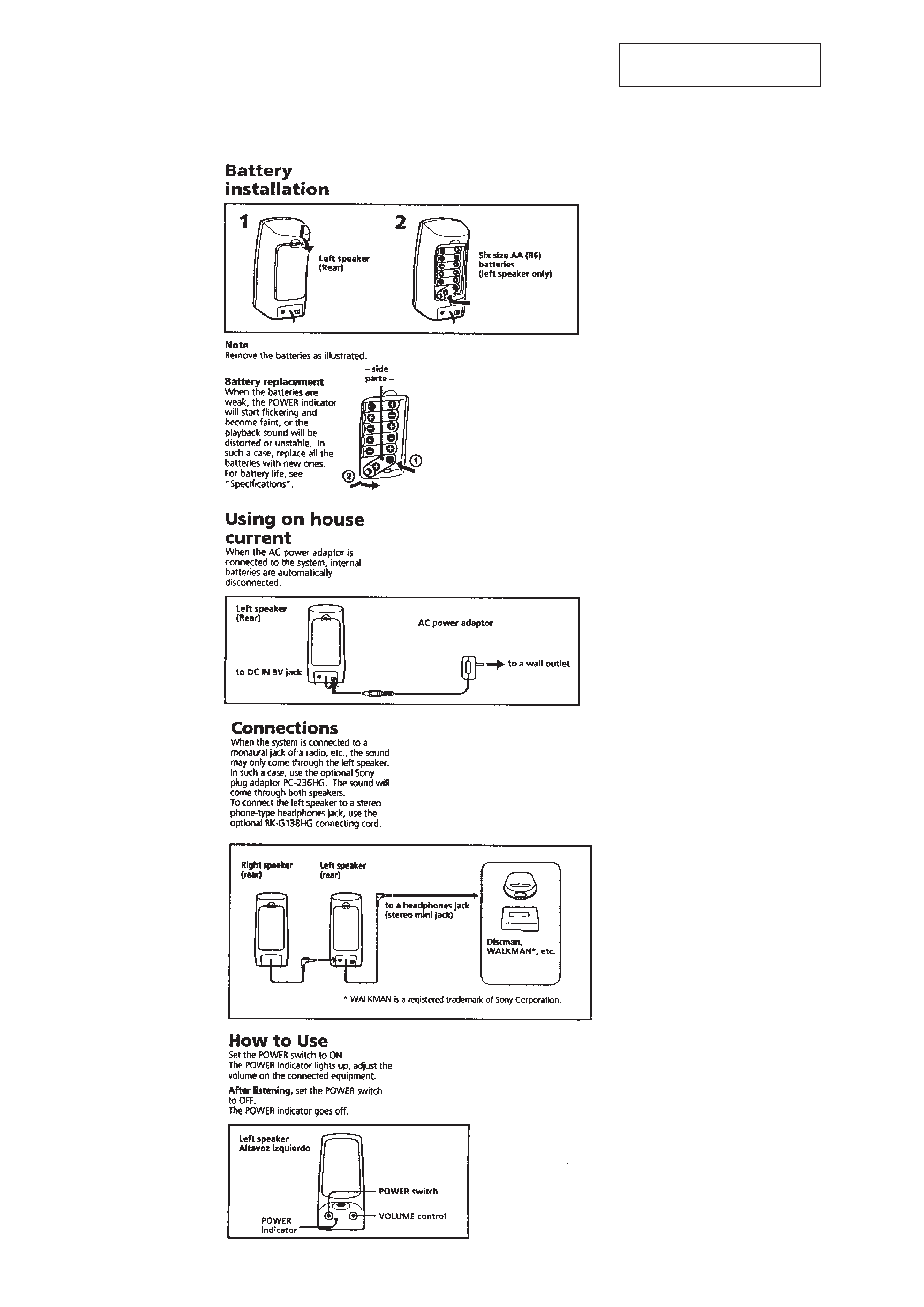
Power requirement
DC 9V, six R6 (size AA) batteries
(left speaker only)
Inputs
Input cord
Left: Stereo mini plug (1.0m)
Right: monaural mini plug (1.0m)
Battery life (at 5 mW + 5 mW output)
Approx. 10 hours with Sony batteries R6P (SR).
Approx. 24 hours with Sony alkaline batteries LR6 (SG).
Dimensions
Approx. 85 x 185 x 110 mm
(w / h / d) (3 3/8 x 7 3/8 x 4 3/8 in.)
Mass
Left speaker : Approx. 415g
(15 oz.) not incl. batteries
Approx. 525g (1lb 3 oz.) incl. batteries
Right speaker : Approx. 325g (11 oz.)
Design and specifications are subject to change without notice.
2
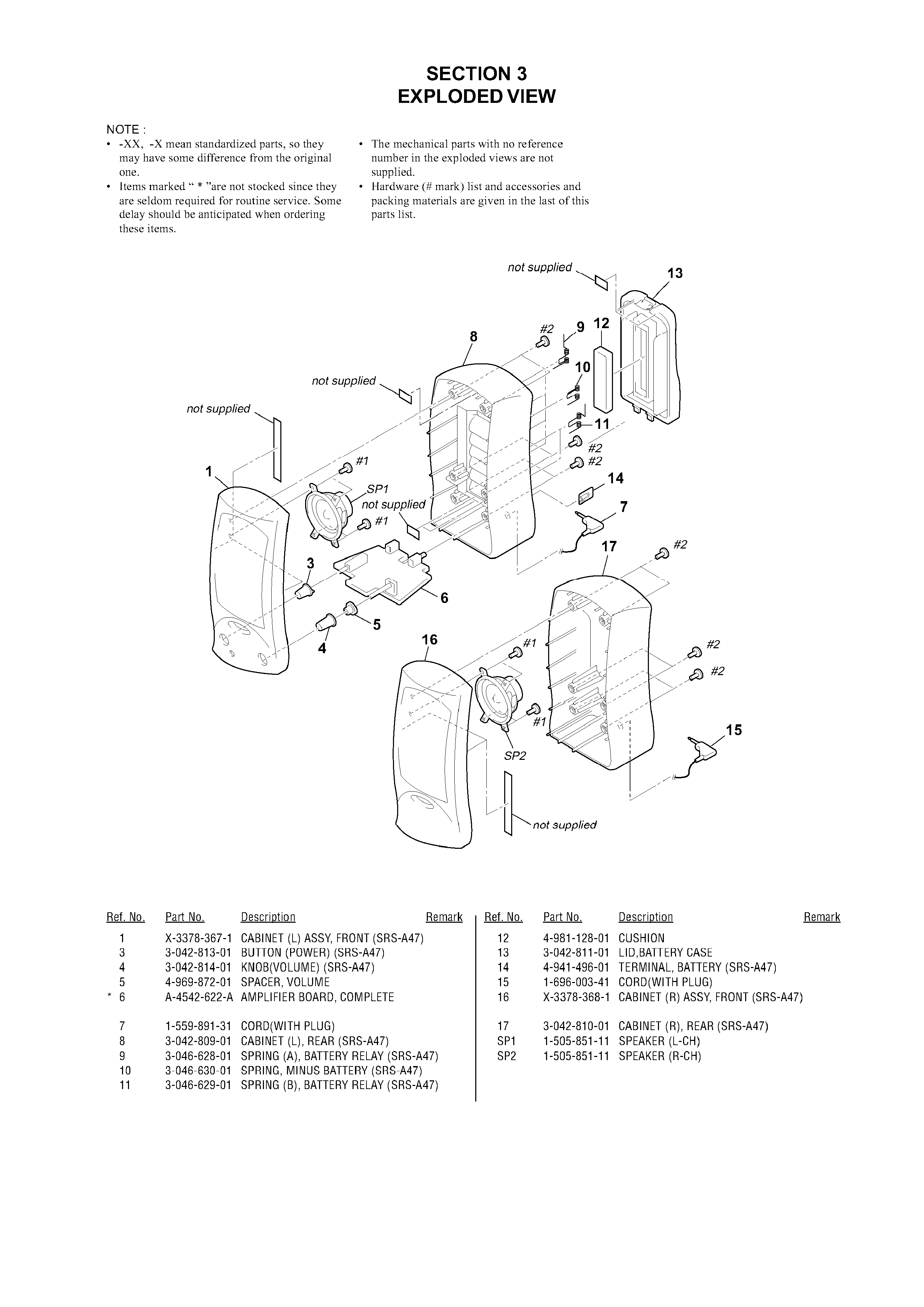
SECTION 1
GENERAL
LOCATION AND FUNCTION OF CONTROLS
This section is extracted from
instruction manual.
02
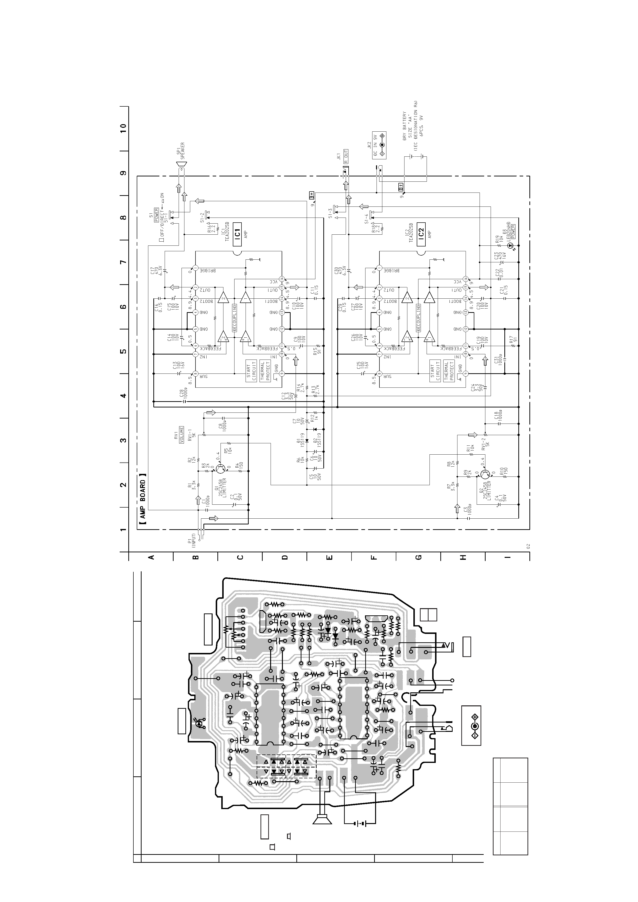
[AMP BOARD]
IC1
IC2
11
(11)
1-677-905-
R18
R16
C17
C14
C26
C30
C13
C25
C5
D3
POWER
C27
C10
C9
C6
C24
C19
C20
C2
C12
C7
C15
C4
R7
R9
R11
R8
D1
D2
R17
R15
R3
R4
R5
R2
R12
R6
J12
J8
J5
R13
R10
R14
R1
R19
J14
J15
J2
J18
C21
C11
C28
C8
C1
C29
C18
C31
C3
J1
J8
J11
J7
J10
J8
J16
C23
C22
J3
J4
J13
J18
C16
E C B
Q1
E
C
B
Q2
J17
DC IN 9V
DRY BATTERY
SIZE "AA"
(IEC DESIGNATION R6)
6PCS, 9V
SP1
SPEAKER
S1
POWER
OFF/DIRECT
R
ON
2
3
4
A
1
B
C
D
S1
-1
-2
-3
-4
1
5
8
9
12
16
1
5
8
9
12
16
+
JK2
P1
(INPUT)
JK1
R OUT
RV1
VOLUME
-1
-2
3
5
4
SRS-A37/A47
2-2. SCHEMATIC DIAGRAM
2-1. PRINTED WIRING BOARDS
Note:
· All capacitors are in
µF unless otherwise noted. pF: µµF
50 WV or less are not indicated except for electrolytics
and tantalums.
· All resistors are in
and 1/4 W or less unless otherwise
specified.
· U : B+ Line.
· Power voltage is dc 9V and fed with regulated dc power
supply from external power voltage jack (JK2).
· Voltages are dc with respect to ground under no-signal
conditions.
· Voltages are taken with a VOM (Input impedance 10 M
).
Voltage variations may be noted due to normal produc-
tion tolerances.
· Signal path.
F
Note:
· X : parts extracted from the component side.
· b : Pattern of the rear side.
D1
C-3
D2
C-3
D3
A-2
Ref. No.
Location
z
Semiconductor Location
Ref. No.
Location
IC1
B-2
IC2
C-2
Q1
B-3
Q2
D-4
SECTION 2
DIAGRAMS