2
SERVICE MANUAL
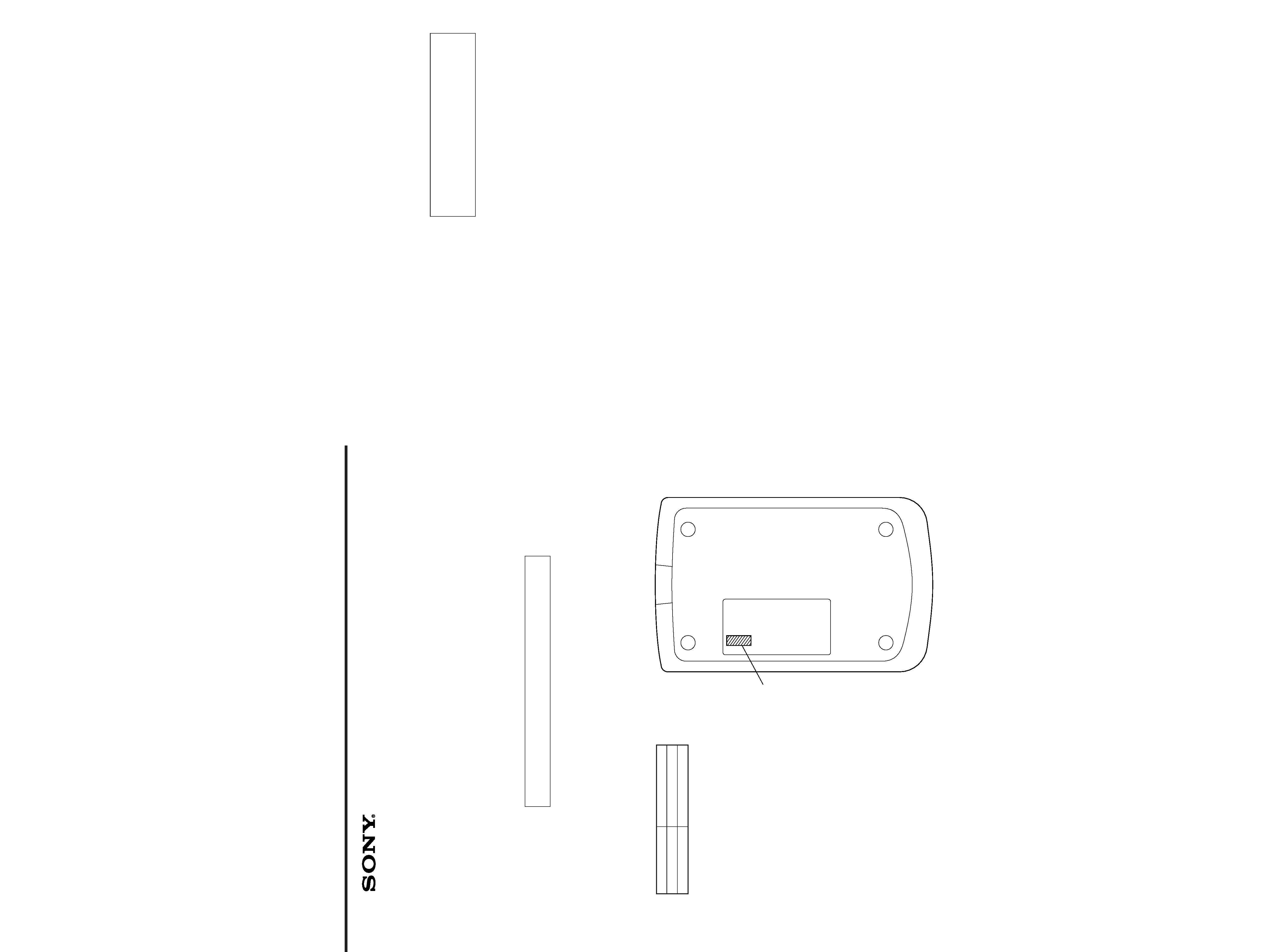
SPP-ID910
US Model
Canadian Model
SUPPLEMENT-4
File this supplement with the service manual.
Subject: BASE MAIN and HAND MAIN board Modification
(ECN-CP801097)
2.
DIAGRAMS
2-1.
NOTE FOR PRINTED WIRING BOARDS
AND SCHEMATIC DIAGRAMS
1.
DISCRIMINATION
On this set, the boards have been changed in the midway of production.
Refer to this service manual supplement-4, if the serial number given on the bottom of the base unit is as listed below.
If the given serial number does not correspond to the following table, refer to original service manual (9-923-970-12) .
Serial Number
Model
Serial Number
US model
550,001 and later
Canadian model
110,001 and later
TABLE OF CONTENTS
1.
DISCRIMINATION .................................................... 1
2.
DIAGRAMS
2-1. Note for Printed Wiring Boards and
Schematic Diagrams .......................................................
2
2-2. Printed Wiring Board BASE (RF) Board ................
3
2-3. Schematic Diagram BASE (RF) Board ....................
5
2-4. Printed Wiring Board BASE (TEL) Board ..............
7
2-5. Schematic Diagram BASE (TEL) Board ................
9
2-6. Printed Wiring Board HAND MAIN Board ........... 11
2-7. Printed Wiring Board
SWITCH SHEET (H/S KEY) ................................. 13
2-8. Schematic Diagram HAND MAIN Board .............. 15
3.
EXPLODED VIEWS ................................................ 17
4.
ELECTRICAL PARTS LIST ............................... 19
Note on Printed Wiring Board:
· X : parts extracted from the component side.
· Y : parts extracted from the conductor side.
· b : Pattern from the side which enables seeing.
(The other layers' patterns are not indicated.)
Caution:
Pattern face side:
Parts on the pattern face side seen from
(Conductor Side)
the pattern face are indicated.
Parts face side:
Parts on the parts face side seen from
(Component Side)
the parts face are indicated.
Note on Schematic Diagram:
· All capacitors are in µF unless otherwise noted. pF: µµF
50 WV or less are not indicated except for electrolytics
and tantalums.
· All resistors are in
and 1/4 W or less unless otherwise
specified.
· 4: printed coil.
· C : panel designation.
· U
: B+ Line.
· H : adjustment for repair.
· Power voltages are dc 9 V and fed with regulated dc power
supply from DC IN 9 V jack (J1) on the BASE (TEL) board,
dc 12 V and fed with regulated dc power supply from TEL
LINE jack (J3) on the BASE (TEL) board with 100
in
series, and dc 3.6 V and fed with regulated dc power sup-
ply from battery terminal on the HAND MAIN board.
· Voltages and waveforms are dc with respect to ground
under no-signal conditions.
no mark : PHONE ON
(
) : PHONE OFF
: Charge (Spare battery)
: Impossible to measure
· Voltages are taken with a VOM (Input impedance 10 M
).
Voltage variations may be noted due to normal produc-
tion tolerances.
· Waveforms are taken with a oscilloscope.
Voltage variations may be noted due to normal produc-
tion tolerances.
· Circled numbers refer to waveforms.
· Signal path.
N
: RX
O
: TX
P
: bell
SPP-ID910
3
4
2-2.
PRINTED WIRING BOARD BASE (RF) Board
· Semiconductor
Location
D1
B-5
D2
B-5
D3
C-3
D8
A-7
D10
C-11
Q1
A-4
Q2
D-11
Q4
D-2
Q5
D-4
Q6
D-3
Q7
D-2
Q8
A-5
Q9
C-3
Q13
A-5
Q15
F-11
Q16
D-10
Q17
F-12
Q18
C-10
Q19
C-11
Q21
B-6
Q22
B-5
Q23
B-5
Q24
C-2
Q28
C-12
Q29
D-12
U1
D-5
U2
C-4
U3
F-7
U4
B-7
U7
B-6
U8
C-9
U10
C-7
U11
A-8
Ref. No.
Location
(Page 8)
1
3
5
4
U4
SPP-ID910
6
5
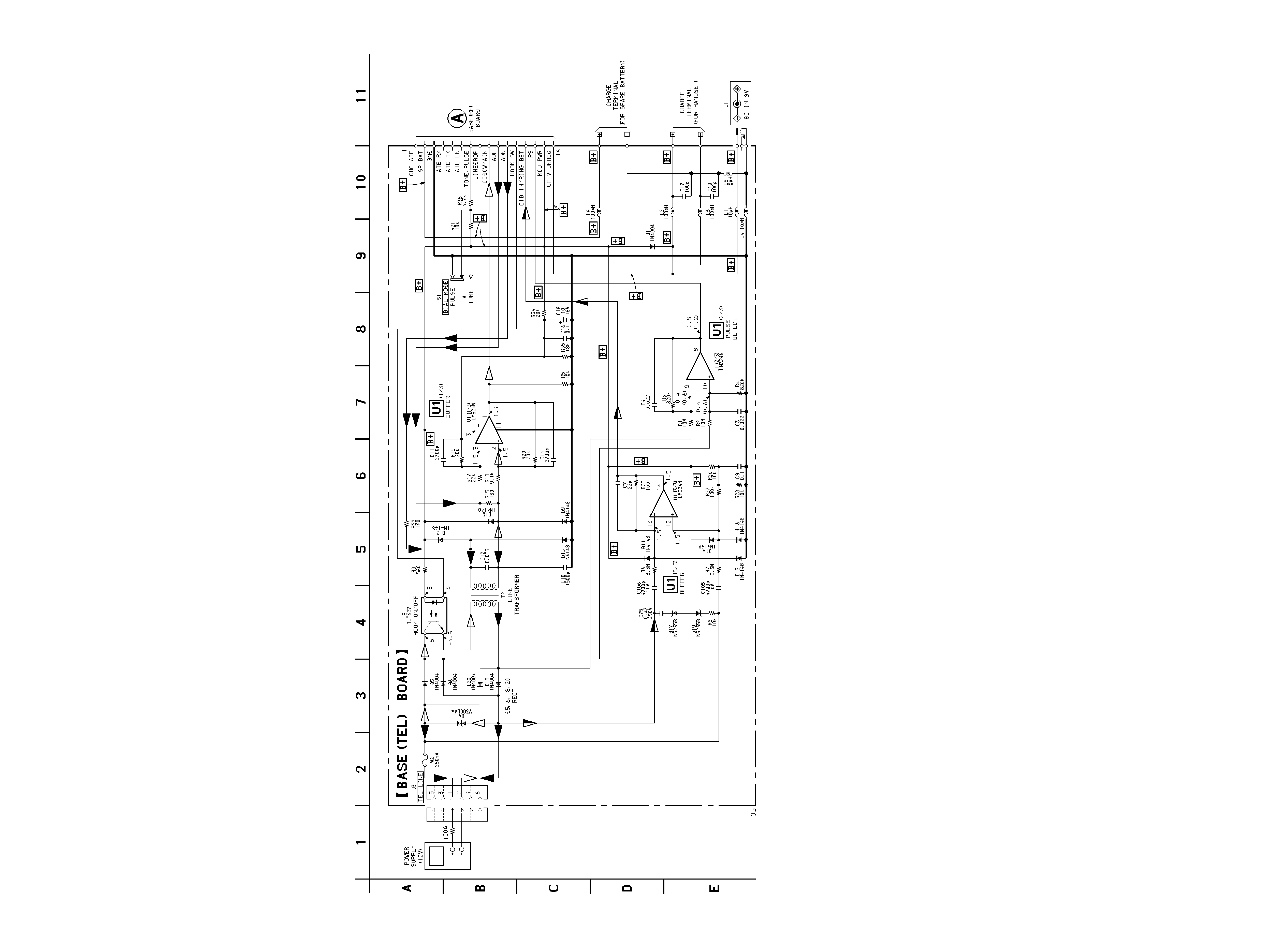
2-3.
SCHEMATIC DIAGRAM BASE (RF) Board
· See page 14 for Waveforms.
(Page
10)
SPP-ID910
7
8
2-4.
PRINTED WIRING BOARD BASE (TEL) Board
(Page 4)
· Semiconductor
Location
D1
E-6
D4
D-2
D5
D-4
D6
D-4
D9
B-3
D10
B-3
D11
D-5
D12
B-3
D13
B-3
D14
D-5
D15
D-5
D16
D-5
D17
D-3
D18
D-3
D19
D-4
D20
D-3
U1
C-5
U3
C-3
Ref. No.
Location
SPP-ID910
9
10
2-5.
SCHEMATIC DIAGRAM BASE (TEL) Baord
(Page 5)