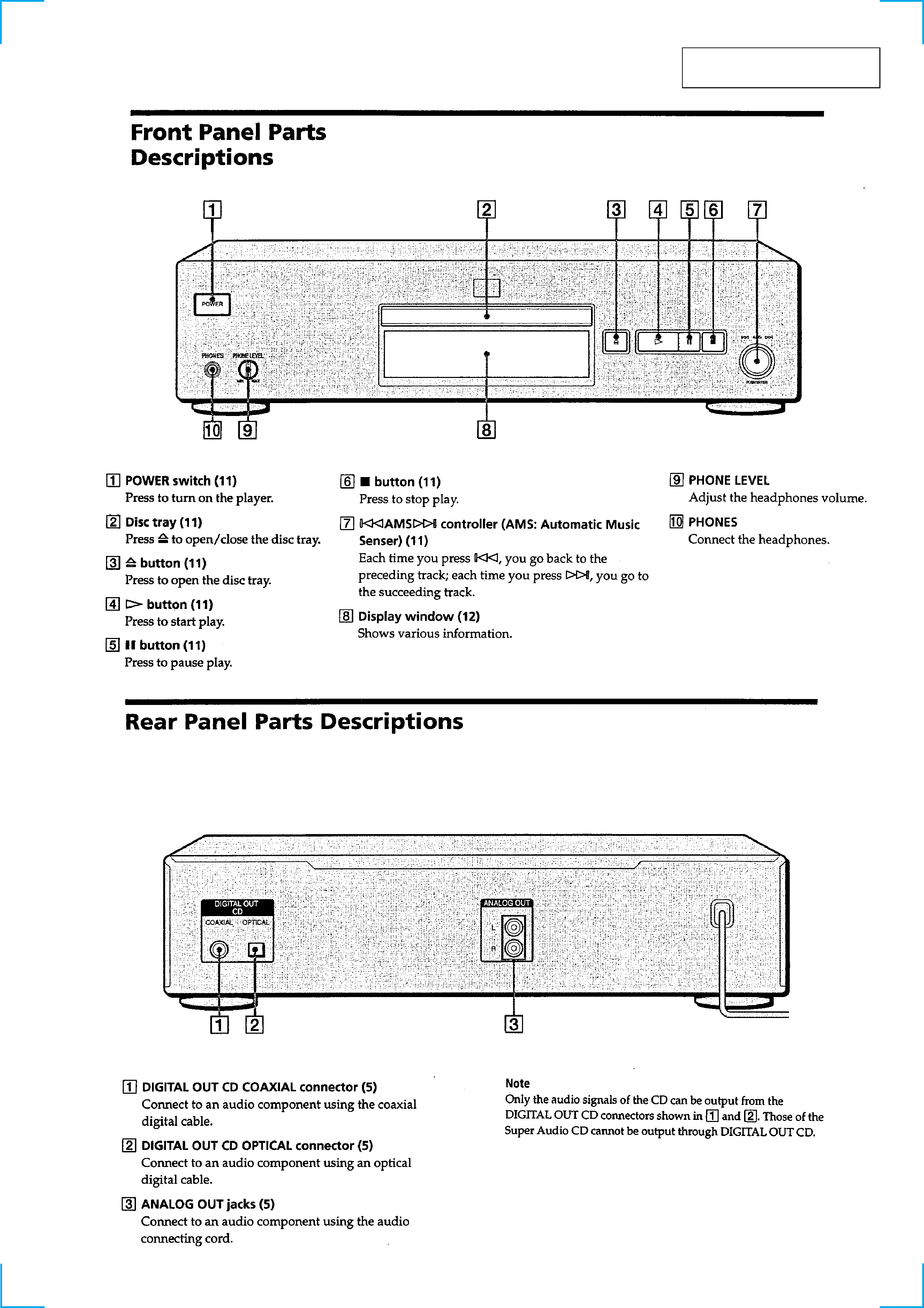
SERVICE MANUAL
SUPER AUDIO CD PLAYER
AEP Model
UK Model
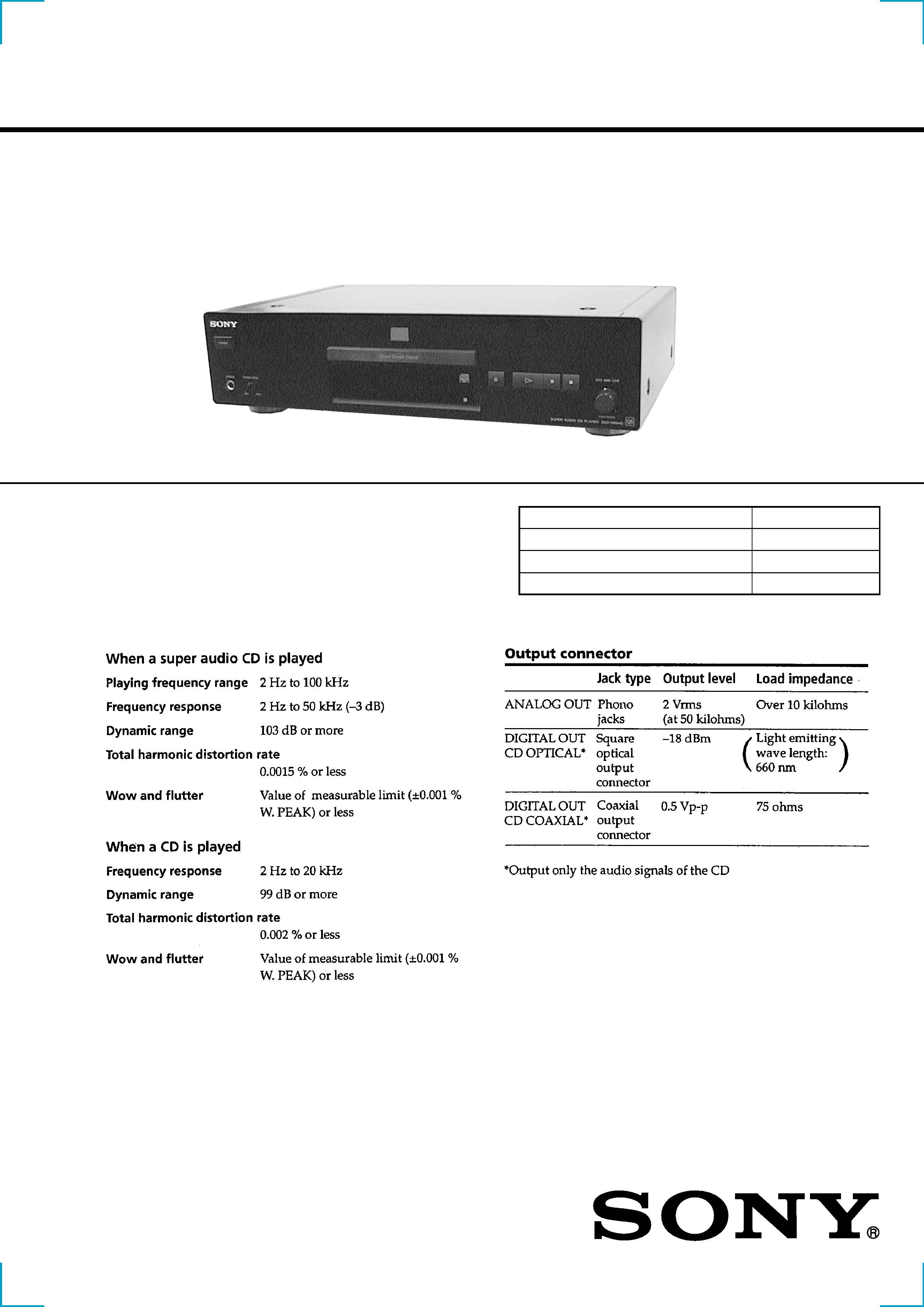
SPECIFICATIONS
SCD-XB940
Model Name Using Similar Mechanism
NEW
CD Mechanism Type
CDM55B-DVBU3
Base Unit Name
DVBU3
Optical Pick-up Name
KHM-220AAA/J1N
Continued on next page
Photo: Black type
Ver 1.1 2002.05
9-929-212-12
Sony Corporation
2002E0500-1
Home Audio Company
C
2002.05
Published by Sony Engineering Corporation
2
SAFETY-RELATED COMPONENT WARNING!!
COMPONENTS IDENTIFIED BY MARK 0 OR DOTTED
LINE WITH MARK 0 ON THE SCHEMATIC DIAGRAMS
AND IN THE PARTS LIST ARE CRITICAL TO SAFE
OPERATION. REPLACE THESE COMPONENTS WITH
SONY PARTS WHOSE PART NUMBERS APPEAR AS
SHOWN IN THIS MANUAL OR IN SUPPLEMENTS PUB-
LISHED BY SONY.
Notes on chip component replacement
· Never reuse a disconnected chip component.
· Notice that the minus side of a tantalum capacitor may be dam-
aged by heat.
Flexible Circuit Board Repairing
· Keep the temperature of the soldering iron around 270 °C dur-
ing repairing.
· Do not touch the soldering iron on the same conductor of the
circuit board (within 3 times).
· Be careful not to apply force on the conductor when soldering
or unsoldering.
CAUTION
Use of controls or adjustments or performance of procedures
other than those specified herein may result in hazardous ra-
diation exposure.

3
TABLE OF CONTENTS
1.
SERVICING NOTES ............................................... 4
2.
GENERAL ................................................................... 5
3.
DISASSEMBLY ......................................................... 8
4.
DIAGRAMS
4-1. Notes for Printed Wiring Board and
Schematic Diagram ......................................................... 11
4-2. Printed Wiring Board TK Board .............................. 12
4-3. Schematic Diagram TK Board ................................ 13
4-4. Printed Wiring Board
MAIN Board (Component Side) .............................. 14
4-5. Printed Wiring Board
MAIN Board (Conductor Side) ................................ 15
4-6. Schematic Diagram MAIN Board (1/6) .................. 16
4-7. Schematic Diagram MAIN Board (2/6) .................. 17
4-8. Schematic Diagram MAIN Board (3/6) .................. 18
4-9. Schematic Diagram MAIN Board (4/6) .................. 19
4-10. Schematic Diagram MAIN Board (5/6) .................. 20
4-11. Schematic Diagram MAIN Board (6/6) .................. 21
4-12. Printed Wiring Board AUDIO Board ...................... 22
4-13. Schematic Diagram AUDIO Board ......................... 23
4-14. Printed Wiring Board HP Board .............................. 24
4-15. Schematic Diagram HP Board ................................. 24
4-16. Printed Wiring Board LOADING Board ................. 25
4-17. Schematic Diagram LOADING Board ................... 25
4-18. Printed Wiring Board DISPLAY Board .................. 26
4-19. Schematic Diagram DISPLAY Board ..................... 27
4-20. Printed Wiring Board POWER Board ..................... 28
4-21. Schematic Diagram POWER Board ........................ 29
4-22. Printed Wiring Boards
AC SW/TRANSFORMER Boards ........................... 30
4-23. Schematic Diagram
AC SW/TRANSFORMER Boards ........................... 31
5.
EXPLODED VIEWS ................................................ 36
6.
ELECTRICAL PARTS LIST ............................... 40
4
The laser diode in the optical pick-up block may suffer electro-
static break-down because of the potential difference generated
by the charged electrostatic load, etc. on clothing and the human
body.
During repair, pay attention to electrostatic break-down and also
use the procedure in the printed matter which is included in the
repair parts.
The flexible board is easily damaged and should be handled with
care.
NOTES ON LASER DIODE EMISSION CHECK
The laser beam on this model is concentrated so as to be focused
on the disc reflective surface by the objective lens in the optical
pick-up block. Therefore, when checking the laser diode emis-
sion, observe from more than 30 cm away from the objective lens.
MODEL IDENTIFICATION
Back Panel
SECTION 1
SERVICING NOTES
NOTES ON HANDLING THE OPTICAL PICK-UP
BLOCK OR BASE UNIT
Part No.
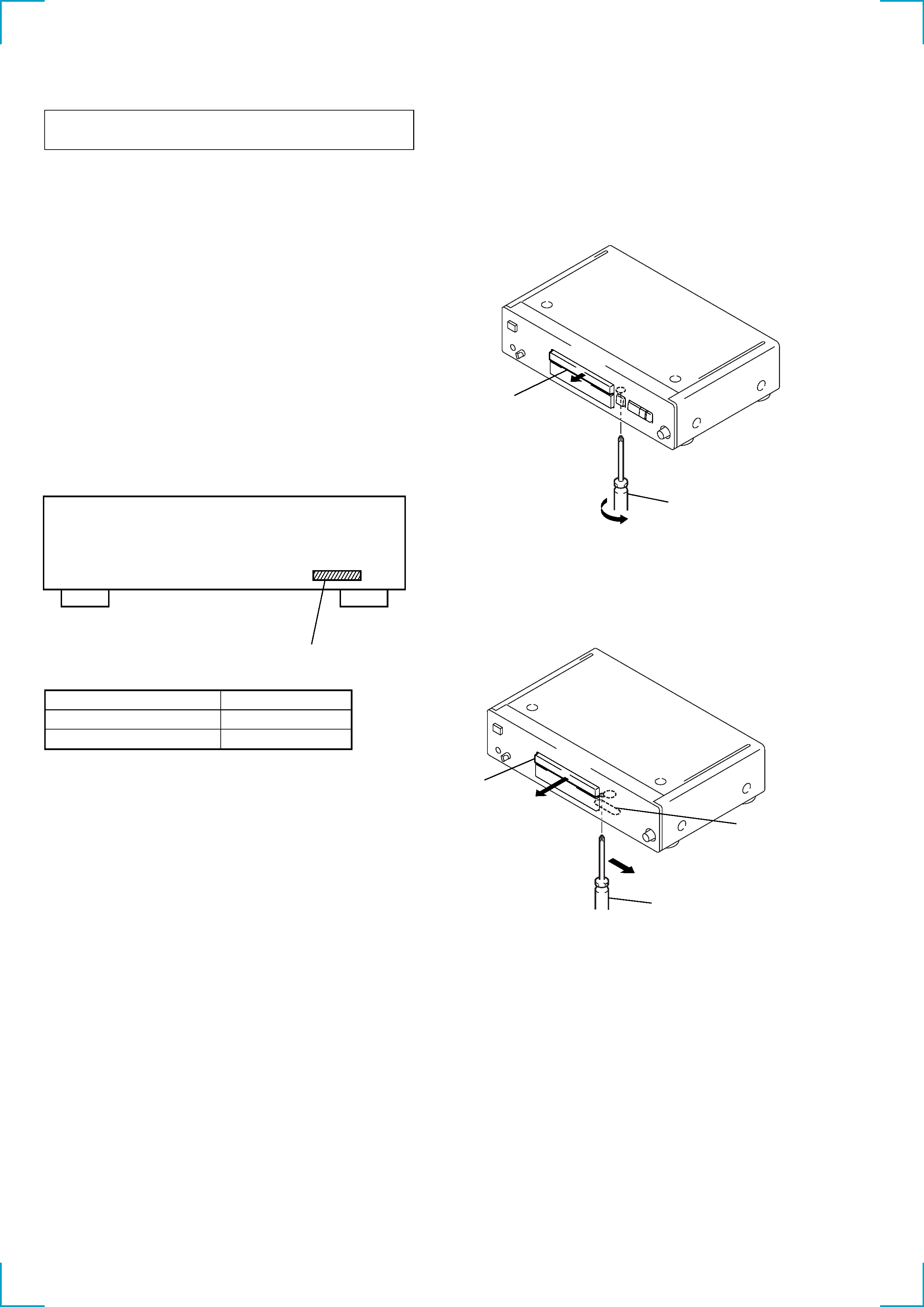
HOW TO OPEN THE TRAY WHEN POWER SWITCH
TURNS OFF
There are two different methods to open the tray.
· Method-1
Insert a screw driver (3) into the aperture of the unit bottom, and
turn it in the direction of the arrow (to OUT direction).
tray
screw driver (3)
* To close the disc table, turn the screw driver (3)
in the reverse direction (to IN direction).
Model
Part No.
AEP
4-227-711-0s
UK
4-227-711-1s
tray
A
B
cam (CDM55)
screw driver (3)
· Method-2
1
Insert a screw driver (3) into the aperture of the unit bottom,
and move the cam (CDM55) in the direction of arrow A.
2
Pull the tray in the direction of arrow B.
ABOUT THE "E01" DISPLAY
"E01" is displayed when the above occurs in communication with
a system controller (IC605) and a display controller (IC203) at the
time of starting.
In this case, please check soldering, disconnection, etc. of each
IC.
Ver 1.1
5
SECTION 2
GENERAL
This section is extracted from
instruction manual.