SERVICE MANUAL
SUPER AUDIO CD PLAYER
AEP Model
UK Model
Korean Model
SCD-XB780
Ver 1.3 2002.11
SPECIFICATIONS
Model Name Using Similar Mechanism
NEW
CD Mechanism Type
CDM66B-DVBU6B
Base Unit Name
DVBU-6B
Optical Pick-up Name
KHM-234AMA
9-873-930-04
Sony Corporation
2002K0500-1
Home Audio Company
C
2002.11
Published by Sony Engineering Corporation
2
SCD-XB780
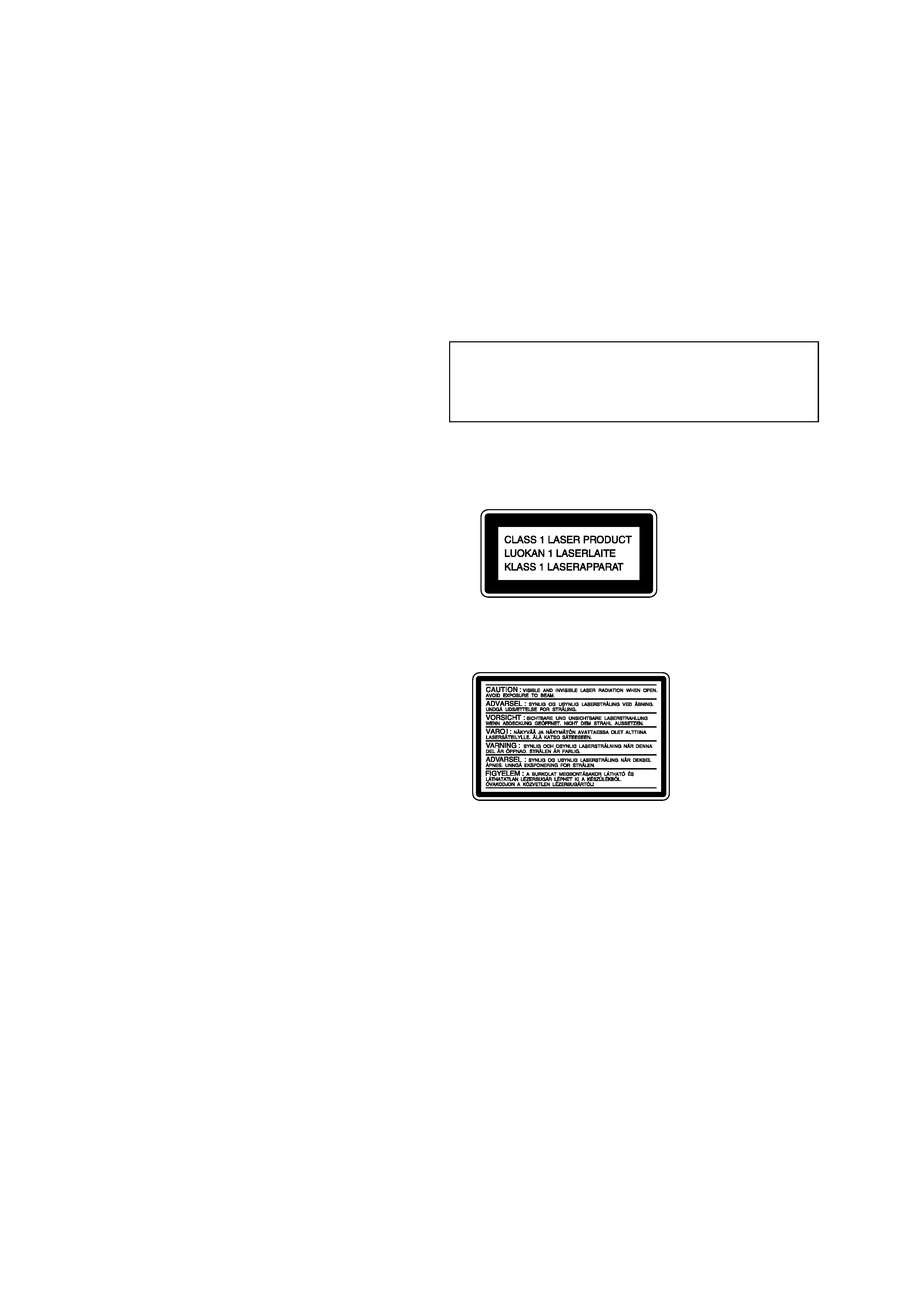
This appliance is classified as a CLASS 1
LASER product.
This label is located on the rear exterior.
The following caution label is located
inside the unit.
SAFETY-RELATED COMPONENT WARNING!!
COMPONENTS IDENTIFIED BY MARK 0 OR DOTTED
LINE WITH MARK 0 ON THE SCHEMATIC DIAGRAMS
AND IN THE PARTS LIST ARE CRITICAL TO SAFE
OPERATION. REPLACE THESE COMPONENTS WITH
SONY PARTS WHOSE PART NUMBERS APPEAR AS
SHOWN IN THIS MANUAL OR IN SUPPLEMENTS PUB-
LISHED BY SONY.
Notes on chip component replacement
·Never reuse a disconnected chip component.
· Notice that the minus side of a tantalum capacitor may be dam-
aged by heat.
Flexible Circuit Board Repairing
·Keep the temperature of the soldering iron around 270 °C dur-
ing repairing.
· Do not touch the soldering iron on the same conductor of the
circuit board (within 3 times).
· Be careful not to apply force on the conductor when soldering
or unsoldering.
TABLE OF CONTENTS
1.
SERVICING NOTES ............................................... 3
2.
GENERAL ................................................................... 6
3.
DISASSEMBLY
3-1. Disassembly Flow ...........................................................
8
3-2. Case .................................................................................
9
3-3. Front Panel Section .........................................................
9
3-4. AUDIO Board, MAIN Board .......................................... 10
3-5. Mechanism Deck (CDM66B-DVBU6B) ....................... 10
3-6. Base Unit (DVBU-6B) .................................................... 11
4.
TEST MODE .............................................................. 12
5.
DIAGRAMS
5-1. Block Diagram RF/SERVO Section ........................ 20
5-2. Block Diagram SERVO Section .............................. 21
5-3. Block Diagram MAIN Section ................................ 22
5-4. Block Diagram AUDIO Section .............................. 23
5-5. Block Diagram DISPLAY/KEY CONTROL/
POWER SUPPLY Section ........................................... 24
5-6. Notes for Printed Wiring Boards and
Schematic Diagrams ....................................................... 25
5-7. Schematic Diagram RF Board ................................. 26
5-8. Printed Wiring Boards
RF/LOADING Boards .............................................. 27
5-9. Printed Wiring Board
MAIN Board (Component Side) .............................. 28
5-10. Printed Wiring Board
MAIN Board (Conductor Side) ................................ 29
5-11. Schematic Diagram
MAIN (1/5)/ LOADING Boards ............................. 30
5-12. Schematic Diagram MAIN Board (2/5) .................. 31
5-13. Schematic Diagram MAIN Board (3/5) .................. 32
5-14. Schematic Diagram MAIN Board (4/5) .................. 33
5-15. Schematic Diagram MAIN Board (5/5) .................. 34
5-16. Schematic Diagram AUDIO/HP Boards ................. 35
5-17. Printed Wiring Board
AUDIO Board (Component Side) ............................ 36
5-18. Printed Wiring Boards
AUDIO (Conductor Side)/HP Boards ..................... 37
5-19. Printed Wiring Boards DISPLAY/KEY Boards ...... 38
5-20. Schematic Diagram DISPLAY/KEY Boards .......... 39
5-21. Printed Wiring Boards
POWER/POWER SW/PT Boards ............................ 40
5-22. Schematic Diagram
POWER/POWER SW/PT Boards ............................ 41
5-23. IC Pin Function Description ........................................... 49
6.
EXPLODED VIEWS
6-1. Case Section .................................................................... 61
6-2. Front Panel Section ......................................................... 62
6-3. Chassis Section ............................................................... 63
6-4. Mechanism Deck Section (CDM66B-DVBU6B) .......... 64
6-5. Base Unit Section (DVBU-6B) ....................................... 65
7.
ELECTRICAL PARTS LIST ............................... 66
CAUTION
Use of controls or adjustments or performance of procedures
other than those specified herein may result in hazardous ra-
diation exposure.
3
SCD-XB780
The laser diode in the optical pick-up block may suffer electro-
static break-down because of the potential difference generated
by the charged electrostatic load, etc. on clothing and the human
body.
During repair, pay attention to electrostatic break-down and also
use the procedure in the printed matter which is included in the
repair parts.
The flexible board is easily damaged and should be handled with
care.
NOTES ON LASER DIODE EMISSION CHECK
The laser beam on this model is concentrated so as to be focused
on the disc reflective surface by the objective lens in the optical
pick-up block. Therefore, when checking the laser diode emis-
sion, observe from more than 30 cm away from the objective lens.
CLEANING OF OPTICAL PICK-UP LENS
In cleaning the lens of optical pick-up, use the air blower.
Never use a cotton swab for cleaning the lens of optical pick-up,
which otherwise causes a trouble.
NOTES ON HANDLING THE OPTICAL PICK-UP
BLOCK OR BASE UNIT
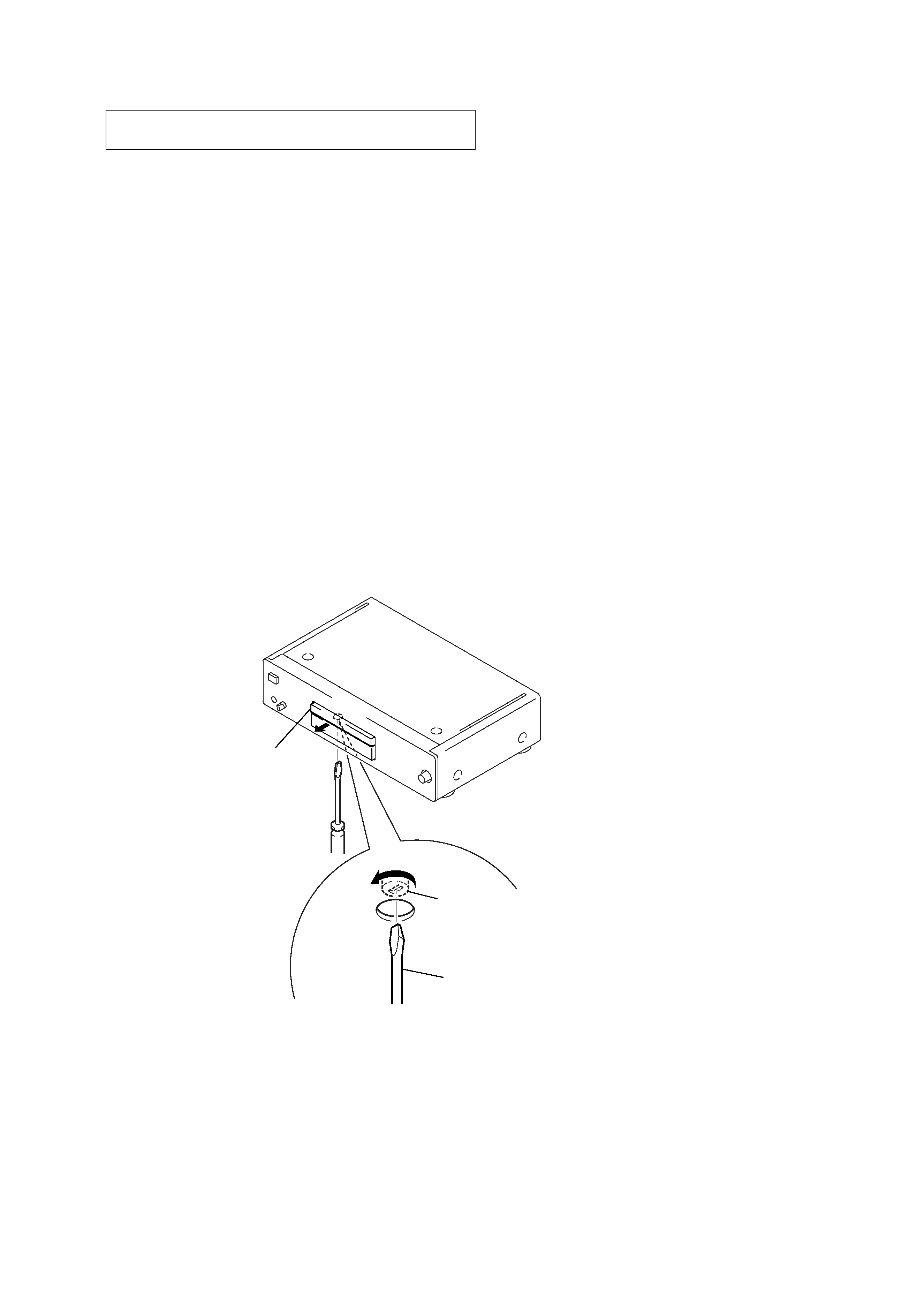
HOW TO OPEN THE TRAY WHEN POWER SWITCH TURNS OFF
tray
tapering driver
cam (66)
1
Insert a tapering driver (3 mm in diameter)
in the hole at the bottom of the unit,
turn the cam (66) fully in the direction of arrow A.
A
SECTION 1
SERVICING NOTES
4
SCD-XB780
DISPLAY BOARD SERVICE POSITION
In checking the DISPLAY board, prepare jig (extension cable J-2501-200-A : 1.00 mm Pitch, 11 cores, Length 300 mm.)
MAIN board
DISPLAY board
CN801
Connect jig (extension cable J-2501-200-A)
to the DISPLAY board (CN801) and
MAIN board (CN706).
CN706
Note: Follow the assembly procedure in the numerical order given.
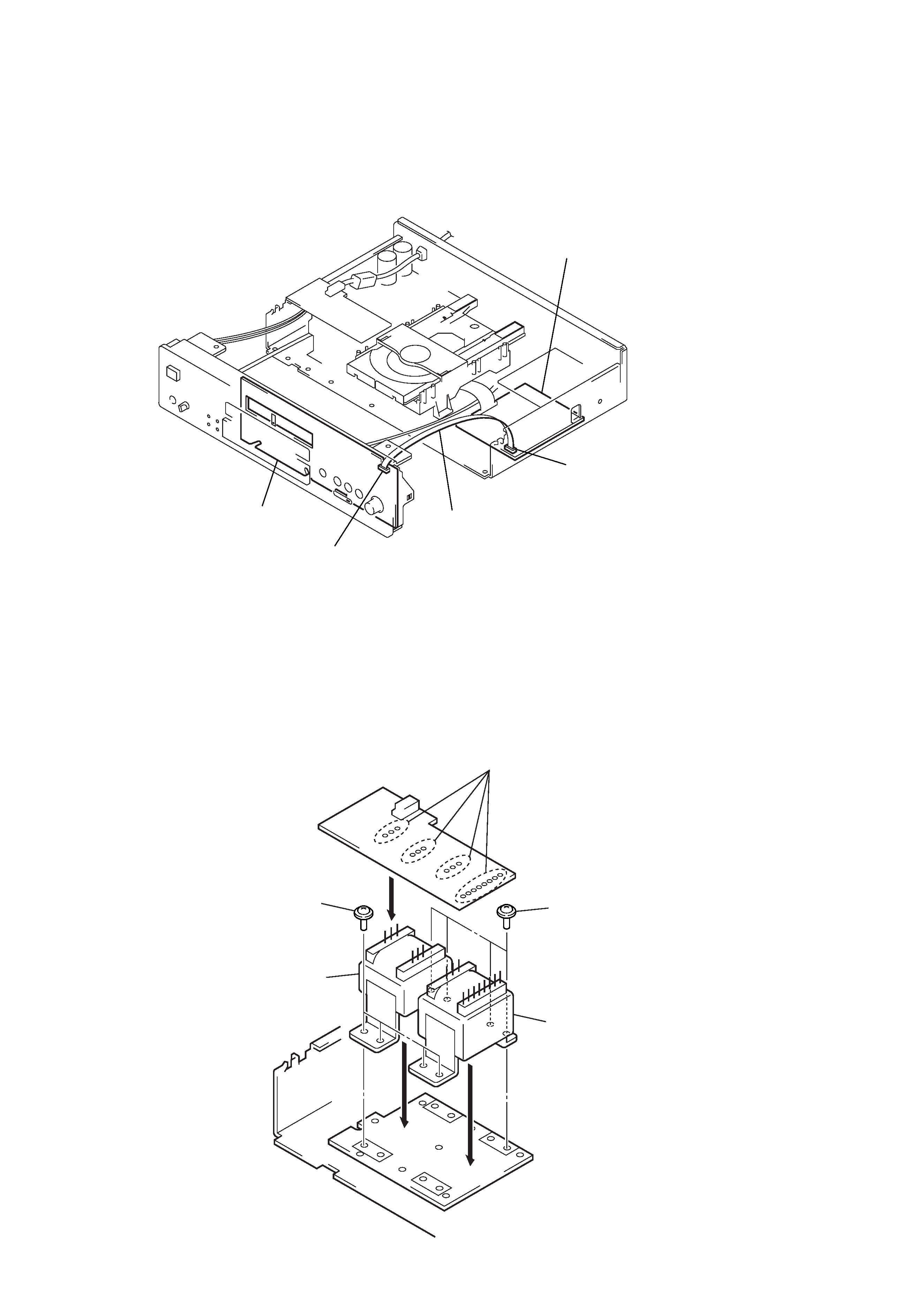
INSTALLATION OF THE TRANS BOARD
3
four screws
(PTTWH3 × 6)
2
power transformer
(T902)
4
3
four screws
(PTTWH3 × 6)
1
power transformer
(T901)
5
Solder seventeen portions.
Note : Solder the TRANS board after installing power transformers (T901, T902)
to the chassis.
(To prevent the TRANS board from being cracked.)

5
SCD-XB780
RESETTING OPERATION AT POWER ON
If the power is turned on with a disc loaded in the set, a sequence of operation as shown below will be performed.
(The operation varies depending on the type of disc)
Condition: continue mode
(1) CD
1.
Sled reverse move (sled in)
2.
Disc detect
3.
IC setting for CD
4.
Servo error signal offset auto adjustment
5.
Spindle kick for LD on
6.
LD on
7.
Focus search
8.
Focus servo on
9.
Spindle kick
10. Spindle servo on
11. E-F balance auto adjustment
12. Tracking & sled servo on
13. Focus bias auto adjustment
14. Focus servo gain auto adjustment
15. Tracking servo gain auto adjustment
16. Jump to lead-in area
17. Read TOC
18. Stop
(2) SACD (single layer)
1.
Sled reverse move (sled in)
2.
Disc detect
3.
IC setting for SACD
4.
Servo error signal offset auto adjustment
5.
Spindle kick for LD on
6.
LD on
7.
Focus search
8.
Focus servo on
9.
Spindle kick
10. Spindle servo on
11. E-F balance auto adjustment
12. Tracking & sled servo on
13. Focus bias auto adjustment
14. Focus servo gain auto adjustment
15. Tracking servo gain auto adjustment
16. Jump to lead-in area
17. Read TOC
18. Stop
(3) SACD (dual layer)
1.
Sled reverse move (sled in)
2.
Disc detect
3.
IC setting for SACD
4.
Servo error signal offset auto adjustment
5.
Spindle kick for LD on
6.
LD on
7.
Focus search
8.
Focus servo on (layer 0)
9.
Spindle kick
10. Spindle servo on
11. E-F balance auto adjustment (layer 0)
12. Tracking & sled servo on (layer 0)
13. Focus bias auto adjustment (layer 0)
14. Focus servo gain auto adjustment (layer 0)
15. Tracking servo gain auto adjustment (layer 0)
16. Jump to lead-in area
17. Read TOC
18. Focus jump (layer 0
tlayer 1)
19. E-F balance auto adjustment (layer 1)
20. Tracking & sled servo on (layer 1)
21. Focus bias auto adjustment (layer 1)
22. Focus servo gain auto adjustment (layer 1)
23. Tracking servo gain auto adjustment (layer 1)
24. Focus Jump (layer 1
tlayer 0)
25. Stop