SERVICE MANUAL
(
)
When a super audio CD is played
Playing frequency range 2 Hz to 100 kHz
Frequency response
2 Hz to 50 kHz (3 dB)
Dynamic range
105 dB or more
Total harmonic distortion rate
0.0012 % or less
Wow and flutter
Value of measurable limit (
±0.001 %
W. PEAK) or less
When a CD is played
Frequency response
2 Hz to 20 kHz
Dynamic range
100 dB or more
Total harmonic distortion rate
0.0017 % or less
Wow and flutter
Value of measurable limit (
±0.001 %
W. PEAK) or less
Output connector
*Output only the audio signals of the CD
General
Laser radiant power:
5.47 uW at 650 nm
*These output is the value measured at a distance of about
200mm from the objective lens surface on the optical pick-up.
Power requirements
230 V AC, 50/60 Hz
Power consumption
26 W
Dimensions (w/h/d)
430
× 130 × 380 mm incl. projecting
parts
Mass (approx.)
14.5 kg
Supplied accessories
Design and specifications are subject to change without notice.
Load impedance
ANALOG OUT
DIGITAL (CD)
OUT OPTICAL*
DIGITAL (CD)
OUT COAXIAL*
Phono
jacks
Jack type
2 Vrms
(at 50 kilohms)
Square
optical
output
connector
18 dBm
0.5 Vp-p
Over 10 kilohms
Light emitting
wave length:
660 nm
Output level
75 ohms
Coaxial
output
connector
PHONES
Stereo
phone jack
32 ohms
20 mW
·Audio connecting cord
(phono jack
× 2 y phono jack × 2) (1)
·Mains lead (1)
·Remote commander (remote) RM-SX90 (1)
·R06 (size-AA) batteries (2)
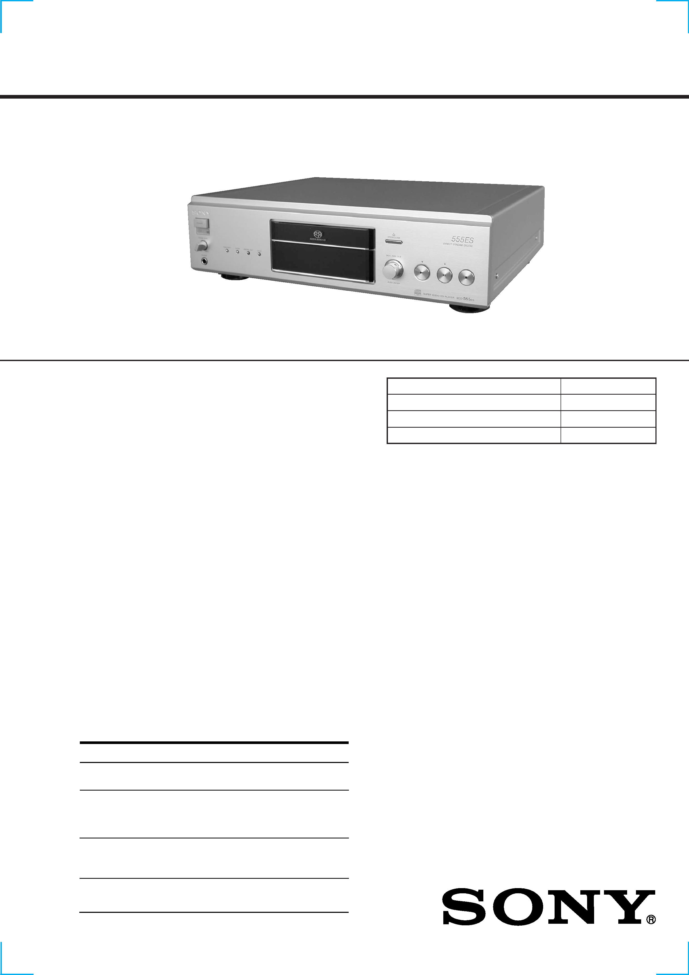
SUPER AUDIO CD PLAYER
AEP Model
SPECIFICATIONS
SCD-555ES
Model Name Using Similar Mechanism
CDP-D500
CD Mechanism Type
CDM19HN-DVBU4
Base Unit Name
DVBU4
Optical Pick-up Name
KHM-230AAA/J1NP
Photo: Gold type
2
SAFETY-RELATED COMPONENT WARNING!!
COMPONENTS IDENTIFIED BY MARK 0 OR DOTTED
LINE WITH MARK 0 ON THE SCHEMATIC DIAGRAMS
AND IN THE PARTS LIST ARE CRITICAL TO SAFE
OPERATION. REPLACE THESE COMPONENTS WITH
SONY PARTS WHOSE PART NUMBERS APPEAR AS
SHOWN IN THIS MANUAL OR IN SUPPLEMENTS PUB-
LISHED BY SONY.
Notes on chip component replacement
· Never reuse a disconnected chip component.
· Notice that the minus side of a tantalum capacitor may be dam-
aged by heat.
Flexible Circuit Board Repairing
· Keep the temperature of the soldering iron around 270 °C dur-
ing repairing.
· Do not touch the soldering iron on the same conductor of the
circuit board (within 3 times).
· Be careful not to apply force on the conductor when soldering
or unsoldering.
TABLE OF CONTENTS
1.
SERVICING NOTES (1) ........................................ 3
2.
GENERAL ................................................................... 6
3.
DISASSEMBLY ......................................................... 9
4.
DIAGRAMS
4-1. Notes for Printed Wiring Boards and
Schematic Diagrams ....................................................... 15
4-2. Printed Wiring Boards
RF/SWITCH/LOADING MOTOR Boards .............. 16
4-3. Schematic Diagram
RF/SWITCH/LOADING MOTOR Boards .............. 17
4-4. Printed Wiring Board
MAIN Board (Component Side) .............................. 18
4-5. Printed Wiring Board
MAIN Board (Conductor Side) ................................ 19
4-6. Schematic Diagram MAIN Board (1/6) .................. 20
4-7. Schematic Diagram MAIN Board (2/6) .................. 21
4-8. Schematic Diagram MAIN Board (3/6) .................. 22
4-9. Schematic Diagram MAIN Board (4/6) .................. 23
4-10. Schematic Diagram MAIN Board (5/6) .................. 24
4-11. Schematic Diagram MAIN Board (6/6) .................. 25
4-12. Printed Wiring Board
AUDIO Board (Component Side) ............................ 26
4-13. Printed Wiring Boards AUDIO (Conductor Side)/
LINE OUT/HEADPHONE Boards ............................. 27
4-14. Schematic Diagram AUDIO Board (1/2) ................ 28
4-15. Schematic Diagram AUDIO (2/2)/LINE OUT/
HEADPHONE Boards ................................................. 29
4-16. Printed Wiring Board DIGITAL OUT Board .......... 30
4-17. Schematic Diagram DIGITAL OUT Board ............ 31
4-18. Printed Wiring Board DISPLAY Board .................. 32
4-19. Schematic Diagram DISPLAY Board ..................... 33
4-20. Printed Wiring Boards
JOG/KEY/R. CNTL Boards ..................................... 34
4-21. Schematic Diagram JOG/KEY/R. CNTL Boards ... 34
4-22. Schematic Diagram
POWER/AC/POWER SWITCH Boards .................. 35
4-23. Printed Wiring Board
POWER Board (Component Side) ........................... 36
4-24. Printed Wiring Boards POWER (Conductor Side)/
AC/POWER SWITCH Boards .................................... 37
4-25. IC Pin Function Description ........................................... 47
5.
SERVICING NOTES (2) ........................................ 59
6.
TEST MODE ............................................................... 60
7.
EXPLODED VIEWS ................................................ 74
8.
ELECTRICAL PARTS LIST ............................... 80
CAUTION
Use of controls or adjustments or performance of procedures
other than those specified herein may result in hazardous ra-
diation exposure.
This appliance is classified as a CLASS 1
LASER product.
The CLASS 1 LASER PRODUCT
MARKING is located on the rear exterior.
The following caution label is located
inside the unit.
3
The laser diode in the optical pick-up block may suffer electro-
static break-down because of the potential difference generated
by the charged electrostatic load, etc. on clothing and the human
body.
During repair, pay attention to electrostatic break-down and also
use the procedure in the printed matter which is included in the
repair parts.
The flexible board is easily damaged and should be handled with
care.
NOTES ON LASER DIODE EMISSION CHECK
The laser beam on this model is concentrated so as to be focused
on the disc reflective surface by the objective lens in the optical
pick-up block. Therefore, when checking the laser diode emis-
sion, observe from more than 30 cm away from the objective lens.
SECTION 1
SERVICING NOTES (1)
NOTES ON HANDLING THE OPTICAL PICK-UP
BLOCK OR BASE UNIT
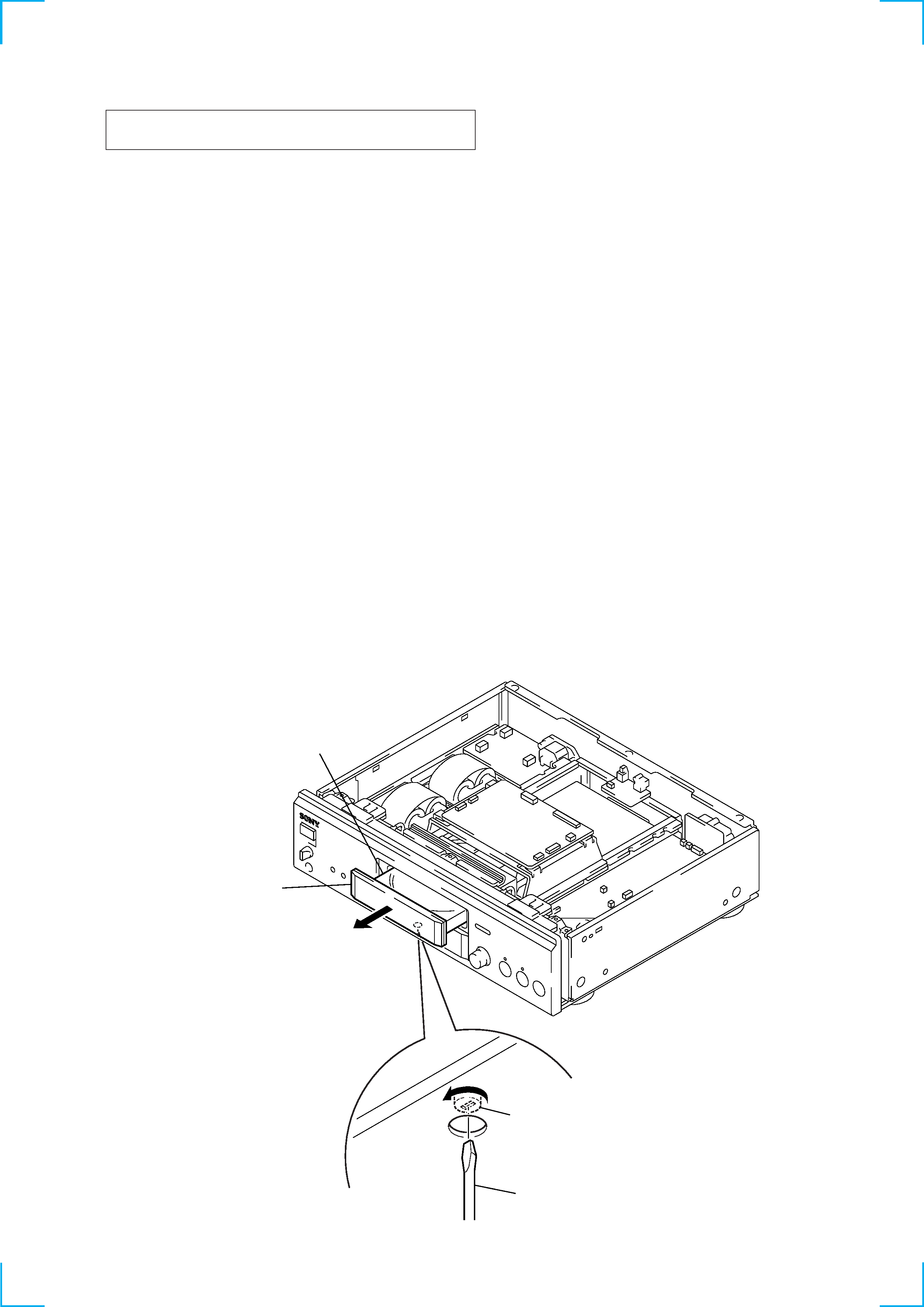
HOW TO OPEN THE DISC TABLE WHEN POWER SWITCH TURNS OFF
disc table
loading panel ass'y
tapering driver
cover (CAM)
2
Draw out the loading panel ass'y
in the direction of arrow B.
1
Insert a tapering driver in the hole
at the bottom of the unit,
turn the cover (CAM) fully in the
direction of arrow A.
B
A
4
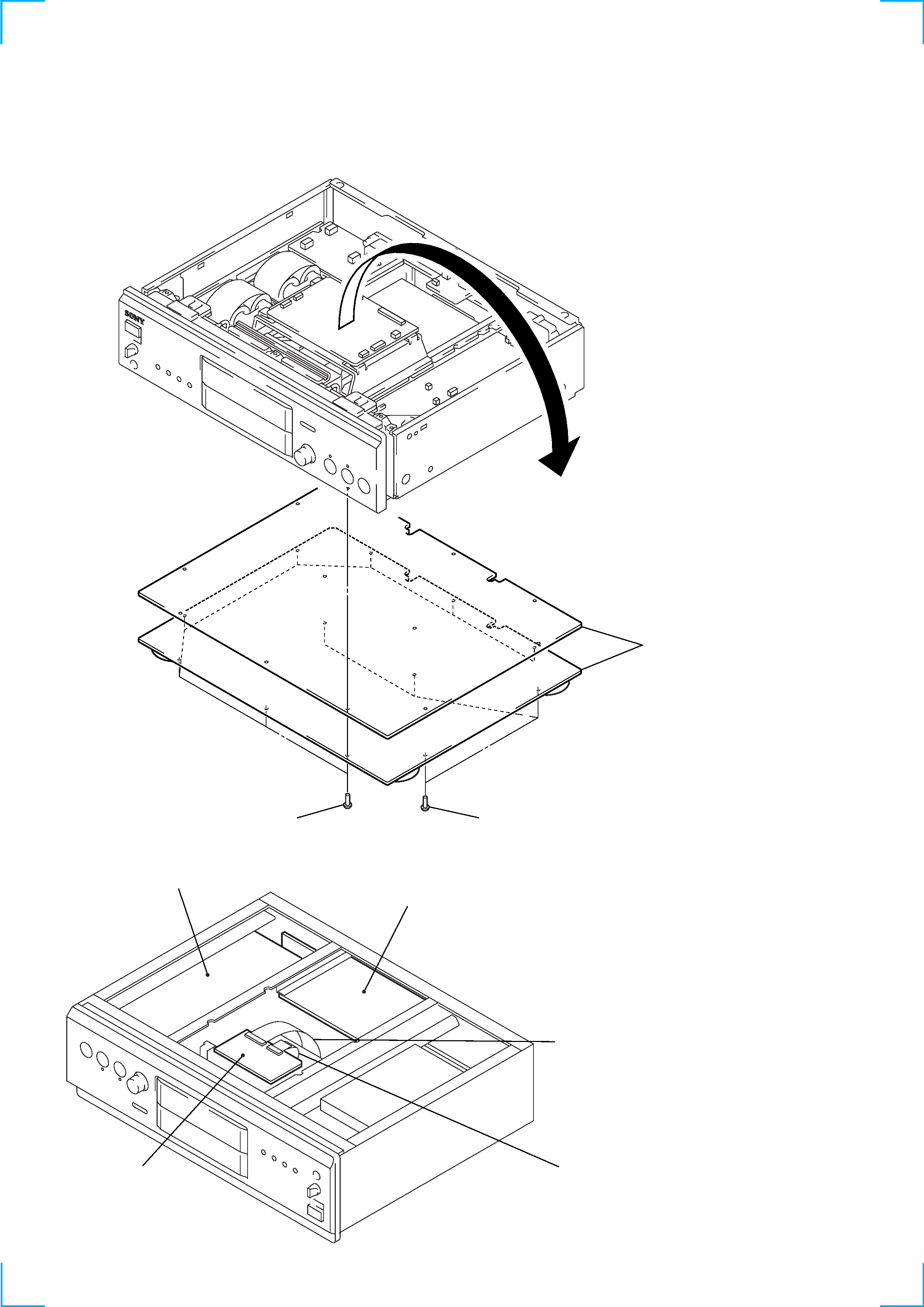
Note: Follow the disassembly procedure in the numerical order given.
AUDIO/POWER BOARDS AND RF BOARD SERVICE POSITION
BOTTOM VIEW
AUDIO board
POWER board
INSTALLATION TWO WIRES (FLAT TYPE) (25/35 CORE)
Note: When the wire (flat type) (35 core) is disconnected
from the RF board, then it is again connected,
disconnect the wire (flat type) (25 core) once,
and reconnect the wire (flat type) (35 core) first.
wire (flat type) (35 core)
wire (flat type) (25 core)
RF board
1
Remove the case.
2
Turn over the set.
4
two bottom plates
3
four screws (3
× 8)
3
eight screws (3
× 8)
5
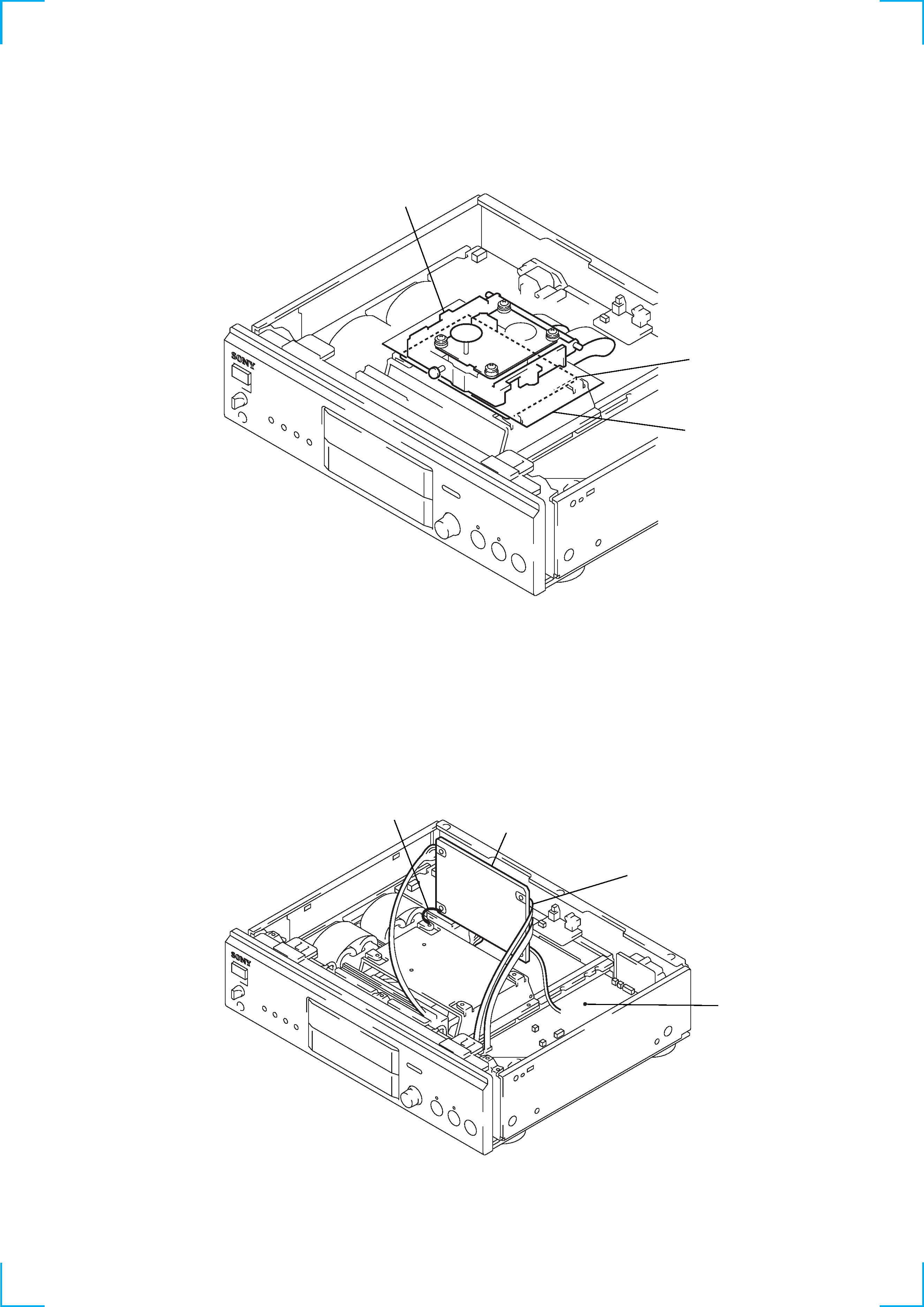
OPTICAL PICK-UP SERVICE POSITION
Place the insulator on the MAIN board, then install the base unit (DVBU4) on it as shown in the figure.
MAIN BOARD SERVICE POSITION
In checking the MAIN board, prepare jig (extension cable J-2501-155-A: 1.00 mm Pitch, 9 cores, Length 300 mm).
Note: Be sure to ground the MAIN board with a lead wire when checking it.
base unit
(DVBU4)
MAIN board
insulator
lead wire
MAIN board
AUDIO board
connect jig (extension cable
J-2501-155-A) to the MAIN
board (CN902) and AUDIO
board (CN308).