Ver 1.0 1999.07
MICROFILM
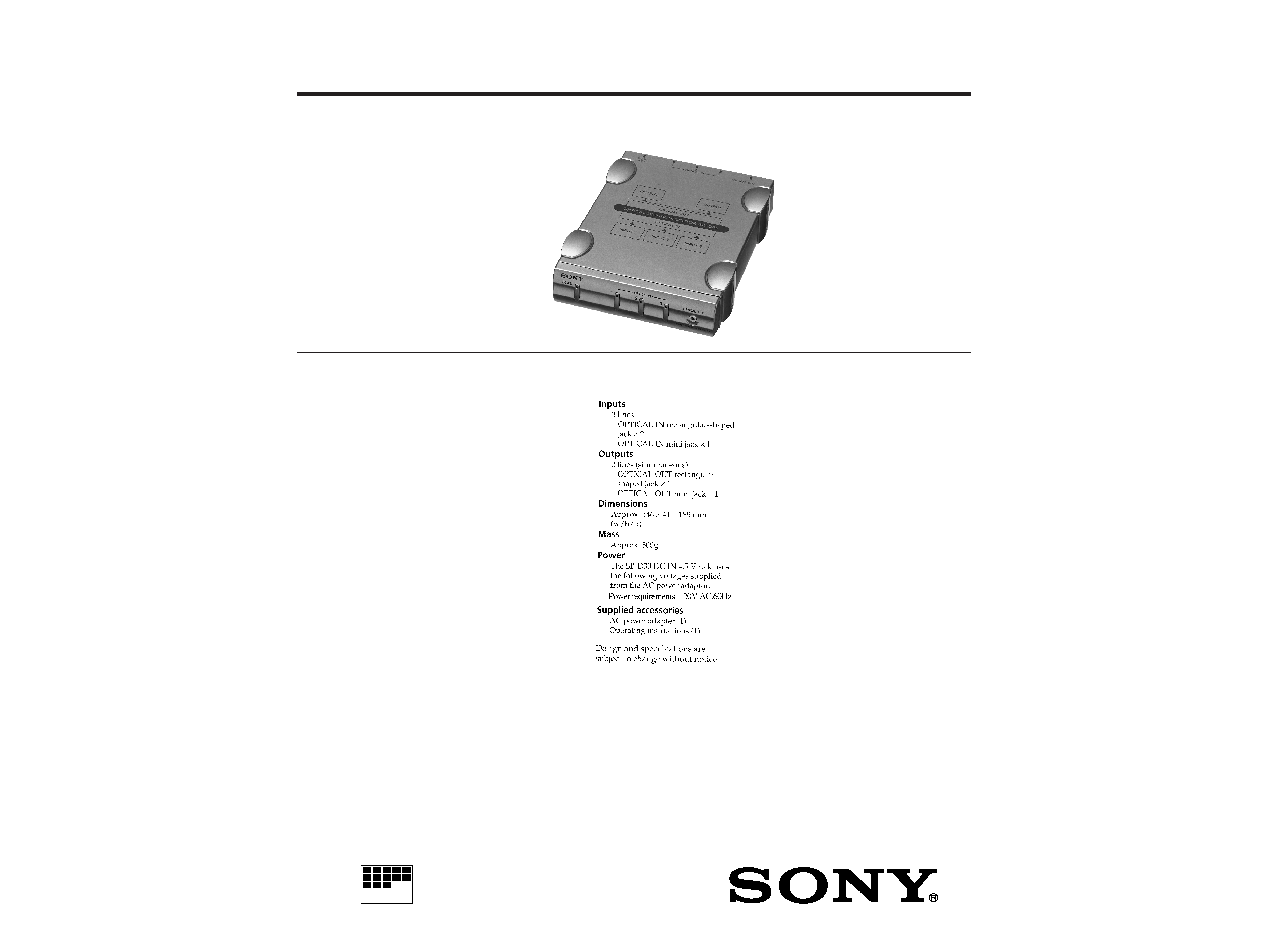
SB-D30
SERVICE MANUAL
OPTICAL DIGITAL SELECTOR
SPECIFICATIONS
US Model
2
Specifications ........................................................................... 1
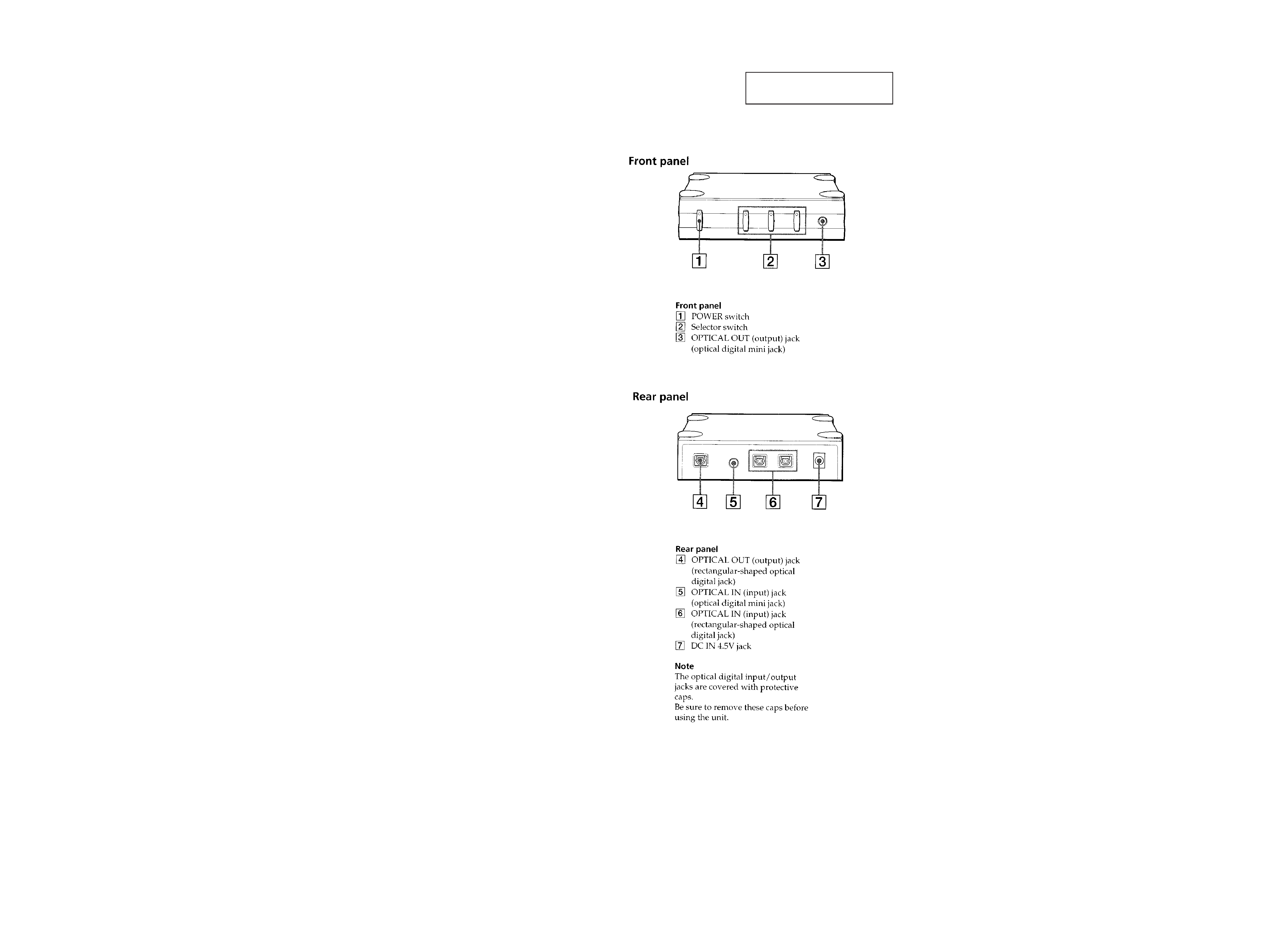
1. GENERAL
Location and Function of Controls .................................... 2
2. DISASSEMBLY
2-1. Cabinet (Lower) .......................................................... 3
2-2. Front panel .................................................................. 3
2-3. Main Board ................................................................. 4
3. DIAGRAMS
3-1. Printed Wiring Boards ................................................ 5
3-2. Schematic Diagram ..................................................... 7
4. EXPLODED VIEW ................................................. 9
5. ELECTRICAL PARTS LIST .................................... 10
Flexible Circuit Board Repairing
· Keep the temperature of the soldering iron around 270°C during
repairing.
· Do not touch the soldering iron on the same conductor of the
circuit board (within 3 times).
· Be careful not to apply force on the conductor when soldering or
unsoldering.
Notes on chip component replacement
· Never reuse a disconnected chip component.
· Notice that the minus side of a tantalum capacitor may be dam-
aged by heat.
TABLE OF CONTENTS
SECTION 1
GENERAL
LOCATION AND FUNCTION OF CONTROLS
This section is extracted from
instruction manual.
3
4
SECTION 2
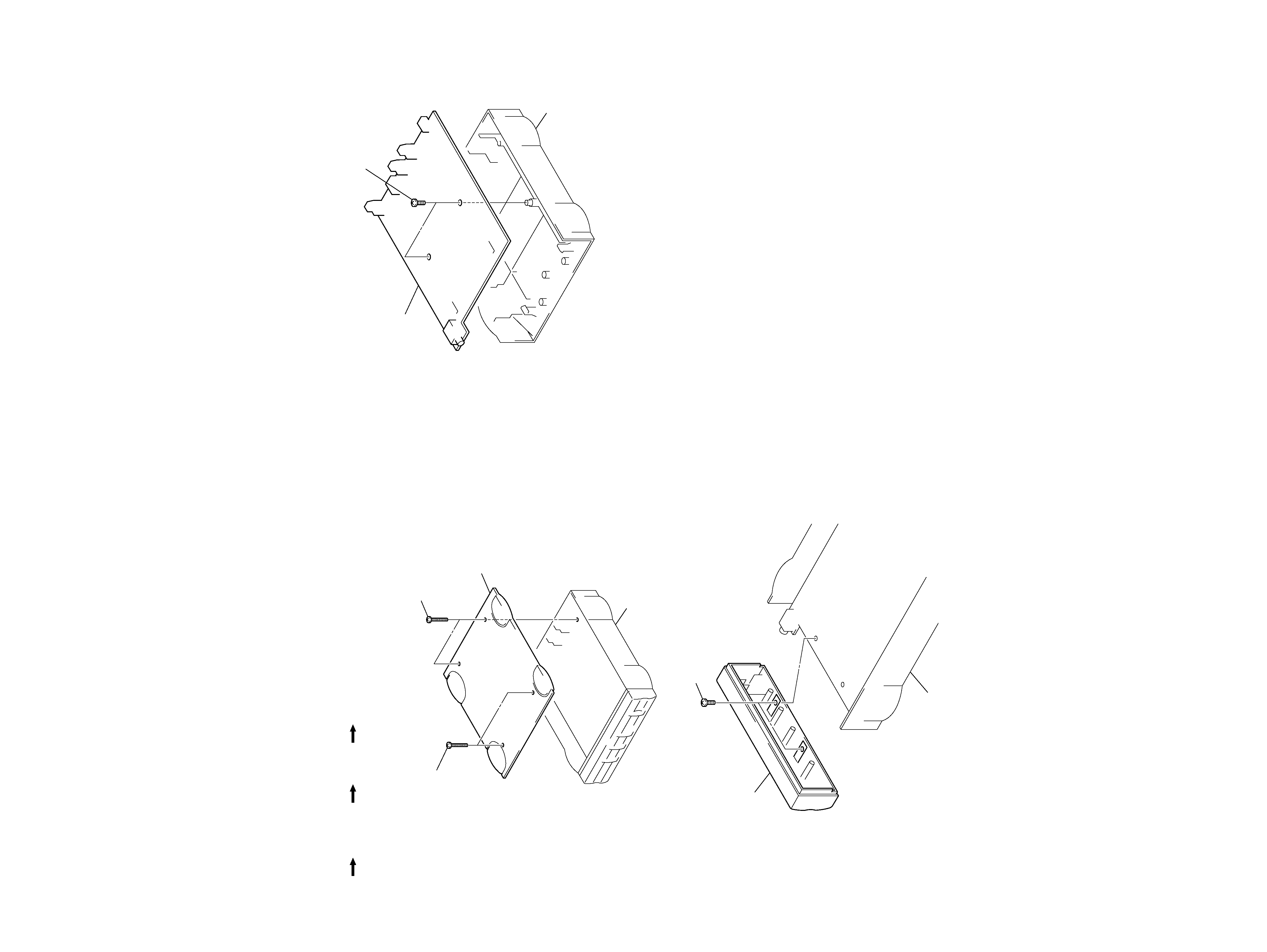
DISASSEMBLY
Note : Follow the disassembly procedure in the numerical order given.
2-1. CABINET (LOWER)
2-2. PANEL, FLONT
r
The equipment can be removed using the following procedure.
Cabinet (Lower)
Set
Panel, Front
Main board
3 Cabinet (Lower)
Cabinet (Upper)
2 Screws (P 2.6x20)
1 Screws (P 2.6x20)
Cabinet (Upper)
1 Screws (P 2.6x8)
2 Panel, Front
2-3. MAIN BOARD
Cabinet (Upper)
1 Screws (P 2.6x8)
2 Main board
5
6
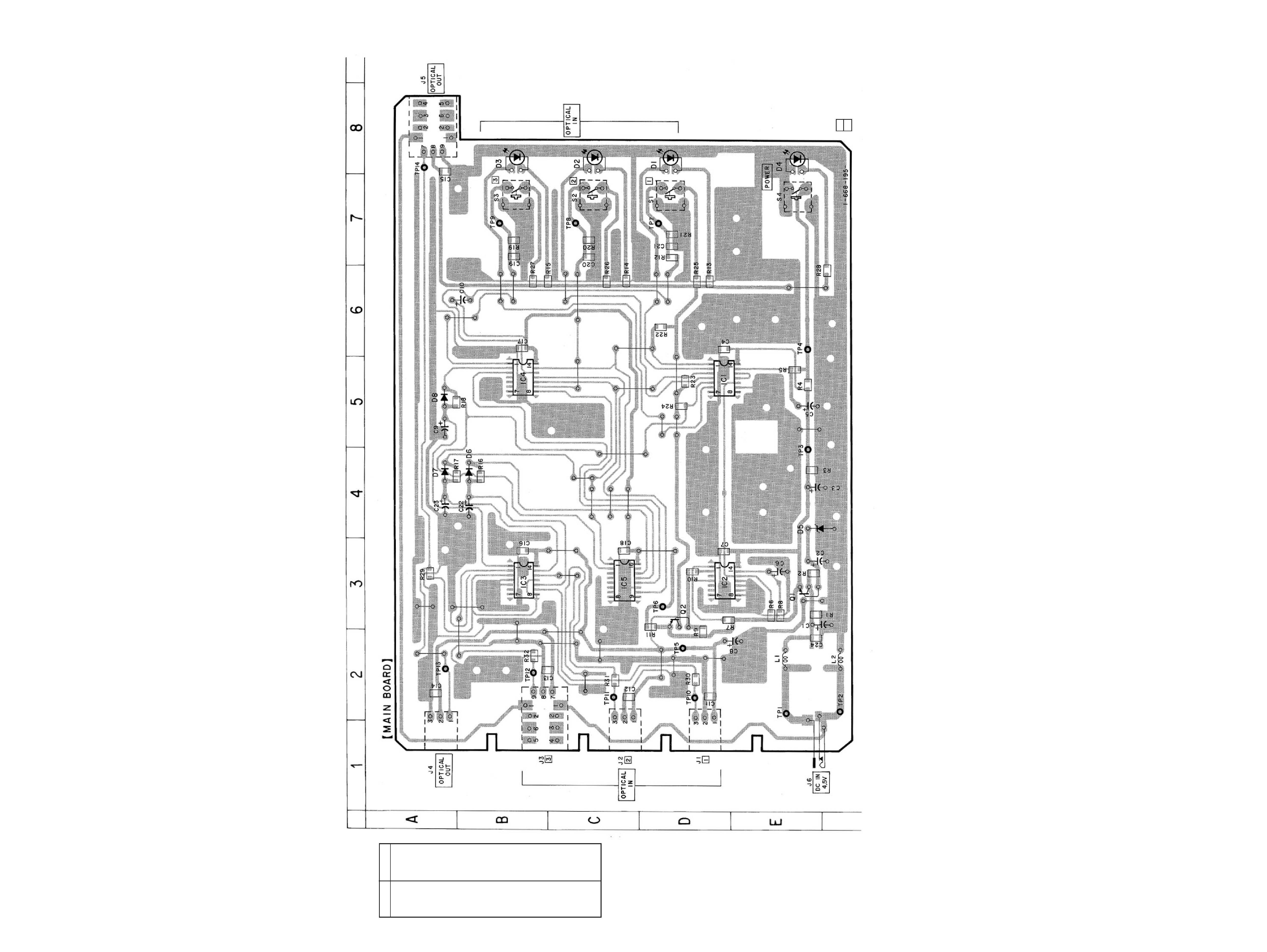
SB-D30
SECTION 3
DIAGRAMS
D1
D-8
D2
C-8
D3
B-8
D4
E-8
D5
E-4
D6
B-4
D7
A-4
D8
A-5
IC1
D-5
IC2
D-3
IC3
B-3
IC4
B-5
IC5
C-3
J1
D-1
J2
C-1
J3
B-1
J4
A-1
J5
A-8
Q1
E-3
Q2
D-3
Ref. No.
Location
r
Semiconductor
Location
3-1. PRINTED WIRING BOARDS
Note:
· X : parts extracted from the component side.
· b : Pattern from the side which enables seeing.
11
(11)
02
7
8
SB-D30
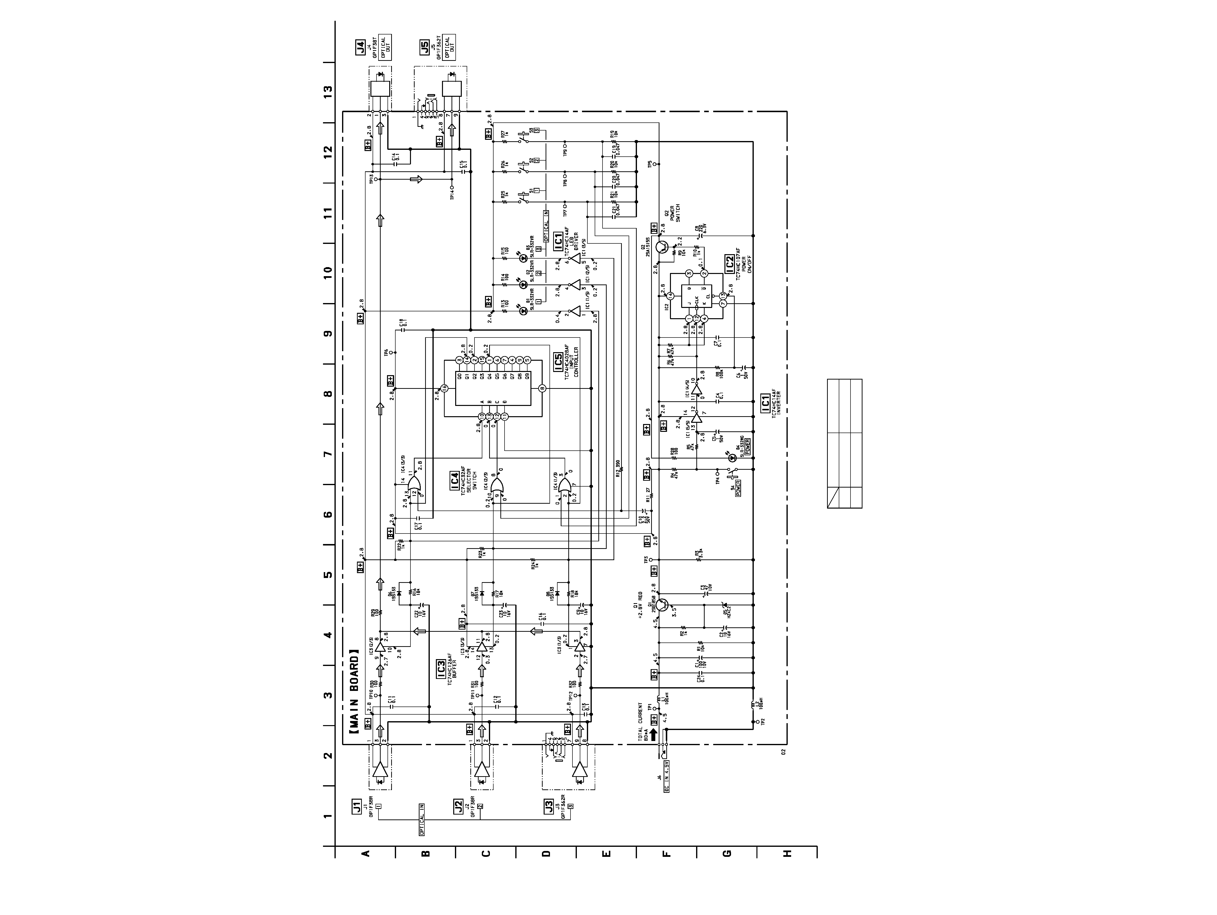
3-2. SCHEMATIC DIAGRAM
TP10,11,12
TP13,14
High
more than 2.1V
less than 0.4V
more than 2.1V
less than 0.8V
Low
Standard Value:
Note:
· All capacitors are in
µF unless otherwise noted. pF: µµF
50 WV or less are not indicated except for electrolytics
and tantalums.
· All resistors are in
and 1/4 W or less unless otherwise
specified.
· U : B+ Line.
· Power voltage is dc 4.5V and fed with regulated dc power
supply from external power voltage jack (J6).
· Voltages are dc with respect to ground under no-signal
conditions.
· Voltages are taken with a VOM (Input impedance 10 M
).
Voltage variations may be noted due to normal produc-
tion tolerances.
· Signal path.
F
: Digital