1
SERVICE MANUAL
US Model
SA-WMSP68
SUB WOOFER
Ver 1.0 2004.07
Sony Corporation
Home Audio Company
Published by Sony Engineering Corporation
9-879-059-01
2004G04-1
© 2004.07
AUDIO POWER SPECIFICATIONS
POWER OUTPUT AND TOTAL HARMONIC
DISTORTION:
With 6 ohm loads, from 28 200 Hz; rated 100
watts, minimum RMS power, with no more than
0.8% total harmonic distortion from 250
milliwatts to rated output.
Speaker system
Active subwoofer,
magnetically shielded
Speaker unit
250 mm cone type
Enclosure type
Acoustically loaded bass
reflex
RMS output
120 W (6 ohms, 100 Hz,
THD 10%)
Input
LINE IN (input pin jacks)
Power requirements
120 V AC, 60 Hz
Power consumption
95 W
Dimensions (w/h/d) (Approx.)
13 3/8
× 16 2/8 × 14 4/8
inches (337
× 410 × 365.5
mm) including front panel
Mass (Approx.)
28 lb 11 oz (13.0 kg)
Design and specifications are subject to change without
notice.
SPECIFICATIONS
· SA-WMSP68 is the subwoofer section
in HT-5800DP/6800DP/DDW960.
2
1.5 k
0.15 µF
AC
voltmeter
(0.75 V)
To Exposed Metal
Parts on Set
Earth Ground
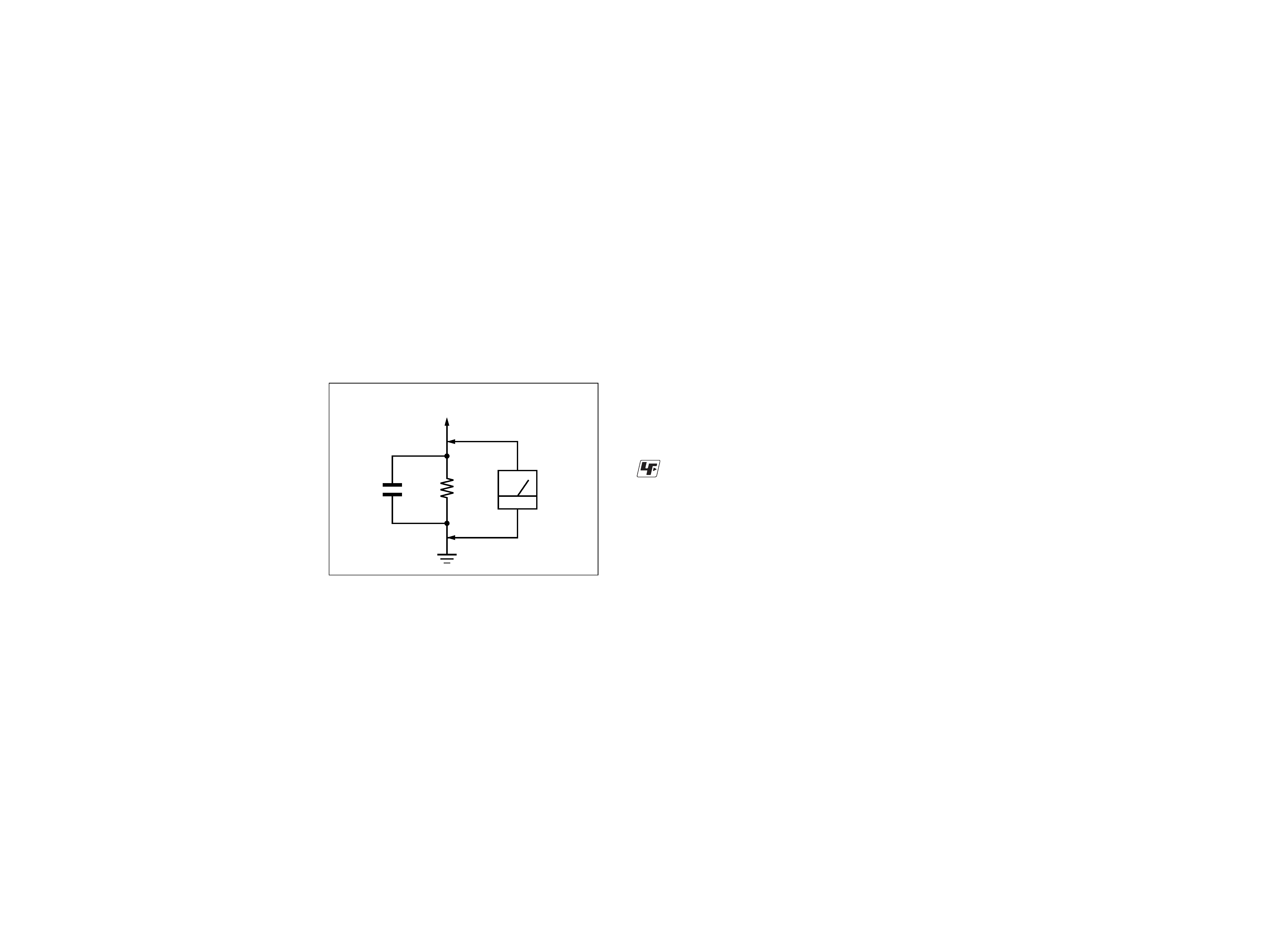
SAFETY CHECK-OUT
After correcting the original service problem, perform the follow-
ing safety check before releasing the set to the customer:
Check the antenna terminals, metal trim, "metallized" knobs, screws,
and all other exposed metal parts for AC leakage.
Check leakage as described below.
LEAKAGE TEST
The AC leakage from any exposed metal part to earth ground and
from all exposed metal parts to any exposed metal part having a
return to chassis, must not exceed 0.5 mA (500 microampers.).
Leakage current can be measured by any one of three methods.
1. A commercial leakage tester, such as the Simpson 229 or RCA
WT-540A. Follow the manufacturers' instructions to use these
instruments.
2. A battery-operated AC milliammeter. The Data Precision 245
digital multimeter is suitable for this job.
3. Measuring the voltage drop across a resistor by means of a
VOM or battery-operated AC voltmeter. The "limit" indica-
tion is 0.75 V, so analog meters must have an accurate low-
voltage scale. The Simpson 250 and Sanwa SH-63Trd are ex-
amples of a passive VOM that is suitable. Nearly all battery
operated digital multimeters that have a 2 V AC range are suit-
able. (See Fig. A)
SAFETY-RELATED COMPONENT WARNING!!
COMPONENTS IDENTIFIED BY MARK 0 OR DOTTED LINE
WITH MARK 0 ON THE SCHEMATIC DIAGRAMS AND IN
THE PARTS LIST ARE CRITICAL TO SAFE OPERATION.
REPLACE THESE COMPONENTS WITH SONY PARTS WHOSE
PART NUMBERS APPEAR AS SHOWN IN THIS MANUAL OR
IN SUPPLEMENTS PUBLISHED BY SONY.
TABLE OF CONTENTS
1. DIAGRAMS
1-1. Note for Printed Wiring Boards and
Schematic Diagrams ............................................................ 3
1-2. Circuit Boards Location ...................................................... 3
1-3. Schematic Diagram Main Section ................................. 5
1-4. Printed Wiring Boards Main Section ............................ 6
2. EXPLODED VIEWS
2-1. Front Section ....................................................................... 7
2-2. Rear Section ........................................................................ 8
3. ELECTRICAL PARTS LIST ........................................... 9
SA-WMSP68
· UNLEADED SOLDER
Boards requiring use of unleaded solder are printed with the lead-
free mark (LF) indicating the solder contains no lead.
(Caution: Some printed circuit boards may not come printed with
the lead free mark due to their particular size.)
: LEAD FREE MARK
Unleaded solder has the following characteristics.
· Unleaded solder melts at a temperature about 40
°C higher than
ordinary solder.
Ordinary soldering irons can be used but the iron tip has to be
applied to the solder joint for a slightly longer time.
Soldering irons using a temperature regulator should be set to
about 350
°C.
Caution: The printed pattern (copper foil) may peel away if
the heated tip is applied for too long, so be careful!
· Strong viscosity
Unleaded solder is more viscous (sticky, less prone to flow)
than ordinary solder so use caution not to let solder bridges
occur such as on IC pins, etc.
· Usable with ordinary solder
It is best to use only unleaded solder but unleaded solder may
also be added to ordinary solder.
(Fig. A)
3
SA-WMSP68
1-1. NOTE FOR PRINTED WIRING BOARDS AND SCHEMATIC DIAGRAMS
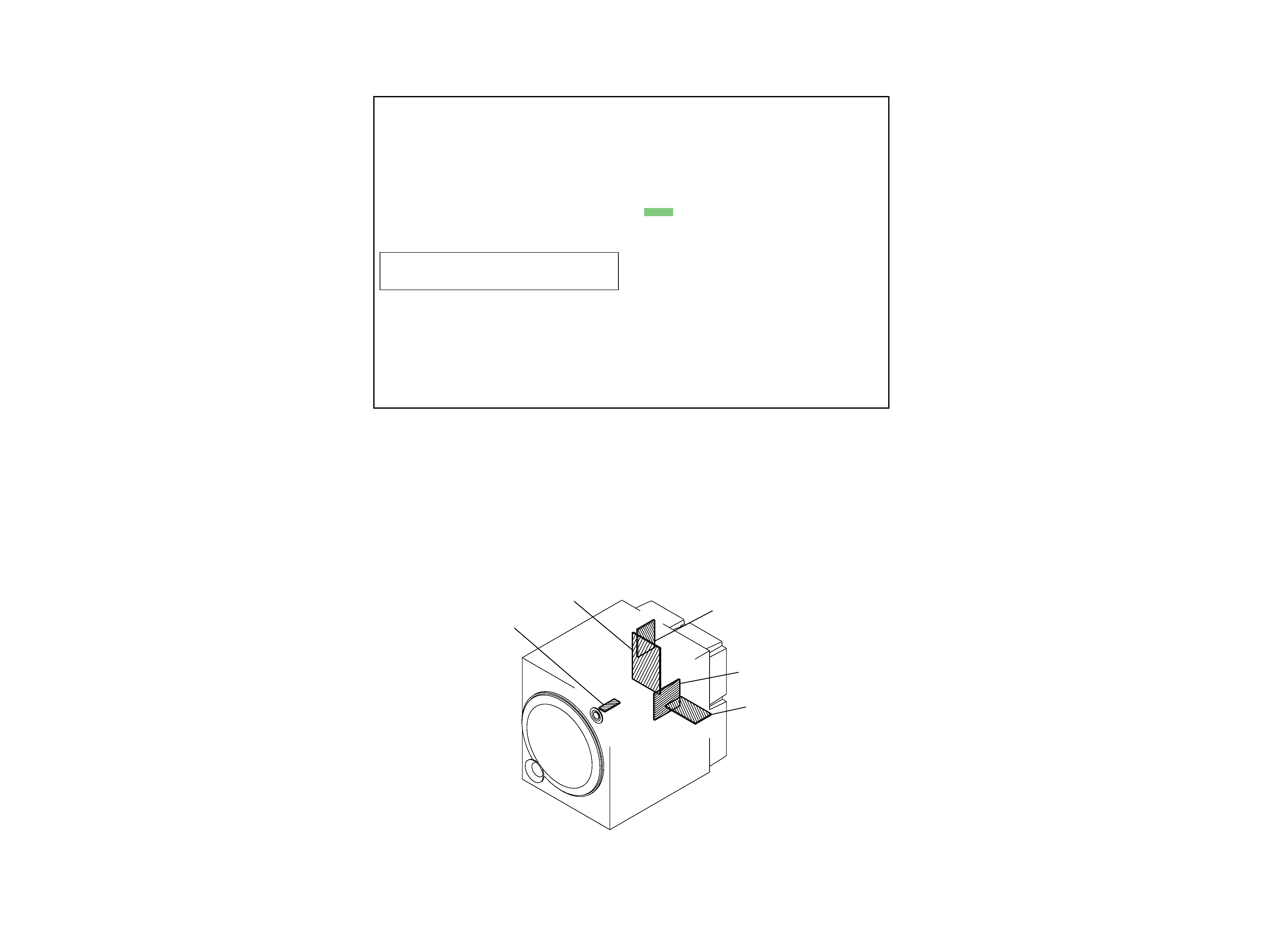
1-2. CIRCUIT BOARDS LOCATION
SECTION 1
DIAGRAMS
THIS NOTE IS COMMON FOR PRINTED WIRING
BOARDS AND SCHEMATIC DIAGRAMS.
(In addition to this, the necessary note is printed
in each block.)
For schematic diagrams.
Note:
· All capacitors are in µF unless otherwise noted. (p: pF)
50 WV or less are not indicated except for electrolytics
and tantalums.
· All resistors are in and 1/4 W or less unless otherwise
specified.
· C : panel designation.
For printed wiring boards.
Note:
· X : parts extracted from the component side.
· Y : parts extracted from the conductor side.
·
: Pattern from the side which enables seeing.
· A : B+ Line.
· B : B Line.
·Voltages are dc with respect to ground under no-signal
(detuned) conditions.
no mark : Power on
·Voltages are taken with a VOM (Input impedance 10 M).
Voltage variations may be noted due to normal produc-
tion tolerances.
· Signal path.
F
: AUDIO
Note: The components identified by mark 0 or dotted line
with mark 0 are critical for safety.
Replace only with part number specified.
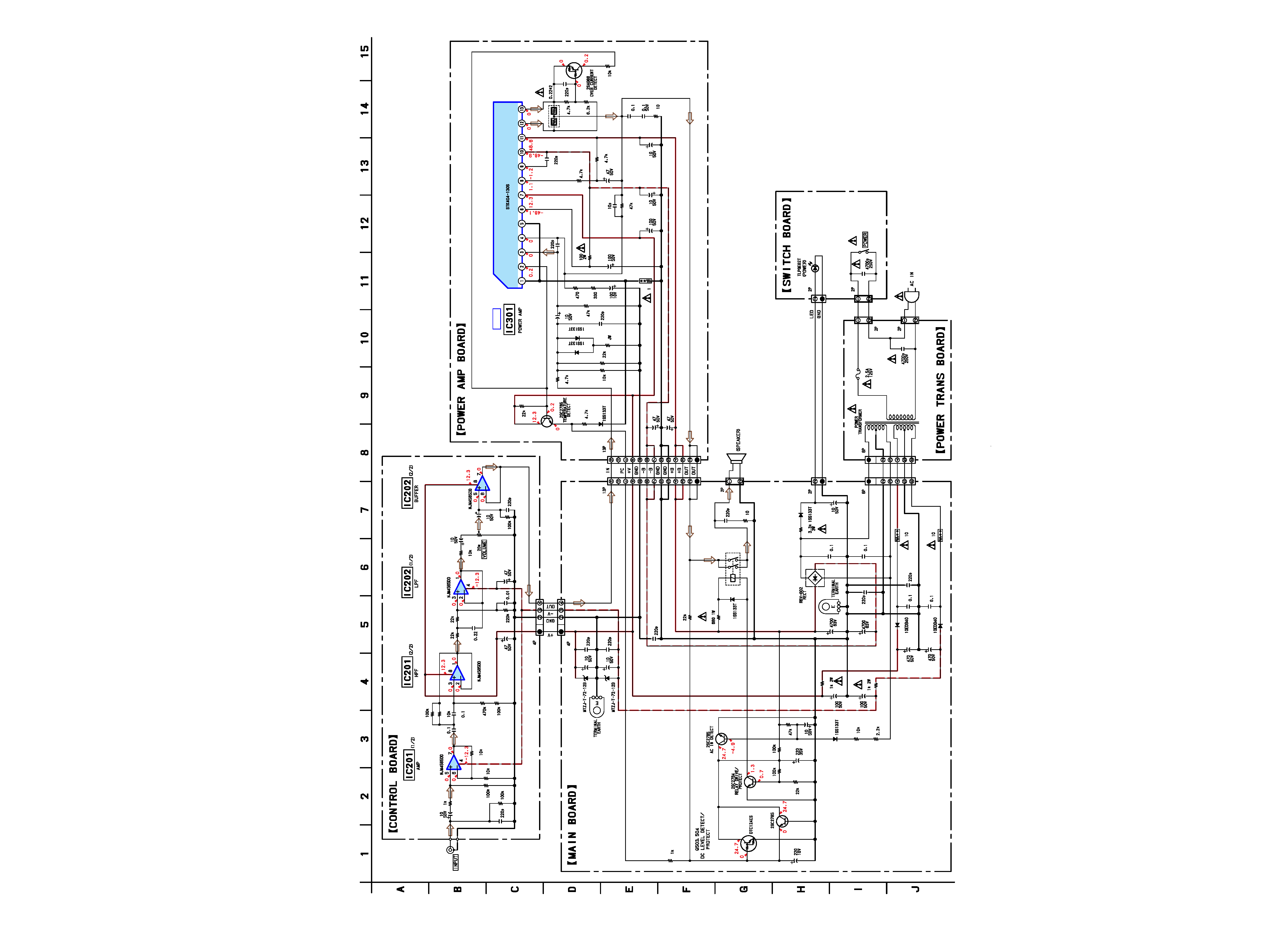
MAIN board
CONTROL board
POWER TRANS board
POWER AMP board
SWITCH board
4
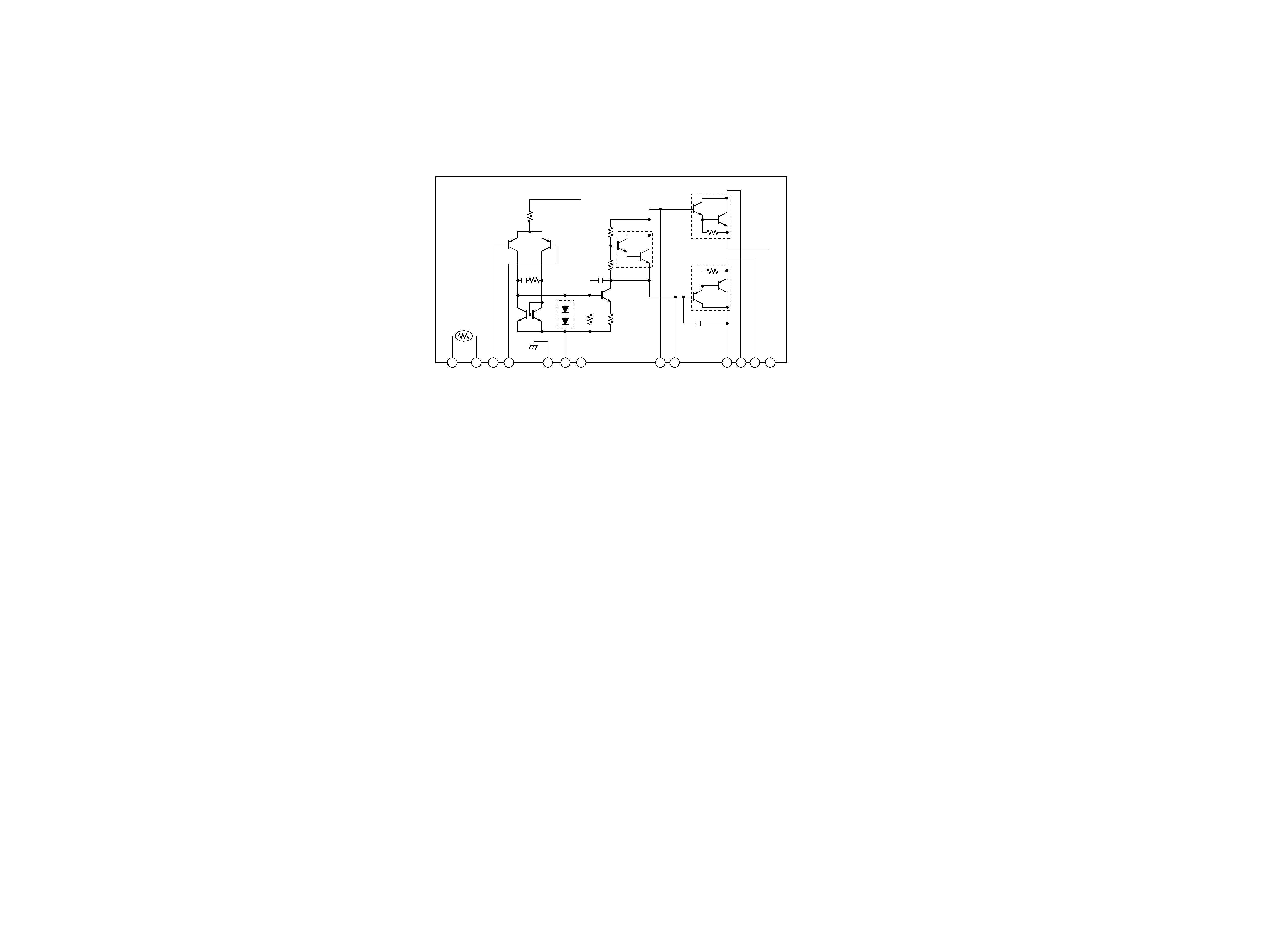
SA-WMSP68
IC301 STK404-130S (POWER AMP Board)
· IC BLOCK DIAGRAM
1
2
3
4
5
6
7
8
9
10
11
12
13
55
SA-WMSP68
1-3. SCHEMATIC DIAGRAM -- MAIN SECTION -- · Refer to page 4 for IC Block Diagram.
IC B/D
J201
C410
C411
S901
C901
R404
R405
C210
C316
C401
C404
C405
C414
C415
D402
D403
IC201(1/2)
IC201(2/2)
IC202(1/2)
IC202(2/2)
IC301
R213
R214
R304
R305
R306
R317
R318
R319
R209
R401
R508
C201
C306
C309
C312
C402
C403
C408
C409
D301
D302
D501
D601
Q503
Q504
R201
R202
R203
R204
R205
R206
R207
R208
R210
R211
R212
R301
R302
R303
R307
R308
R312
R313
R314
R315
R500
R501
R502
R503
R504
R505
R507
R601
R309
C202
C203
C204
C206
C207
C208
C209
C304
C305
C307
C308
C310
C311
C313
C315
C412
C413
C416
C417
C501
C502
C601
C211
C212
CN202
RV201
CN201
C418
C406
C407
R402
R403
C503
C302
C301
CN301
CN302
C303
R310
R311
C314
CN401
CN901
Q302
G2
G1
RY501
Q502
Q501
C1
CN1
F901
T1
CN502
SP901
R316
CN501
D502
Q301
D404
D405
R506
D401
CN101
CN102
CN2
D701
D303