1
Ver 1.1 2002. 08
SERVICE MANUAL
US Model
Canadian Model
AEP Model
UK Model
E Model
SA-VE835ED
For the U.S. model
AUDIO POWER SPECIFICATIONS
POWER OUTPUT AND TOTAL
HARMONIC DISTORTION:
with 3.75 ohm loads both channels driven,
from 20 200 Hz; rated 200 watts per
channel minimum RMS power, with no more
than 0.8% total harmonic distortion from
250 milliwatts to rated output.
SS-MS835 (front, center, and rear speakers)
Speaker system
2 way, magnetically
shielded
Speaker units
Tweeter: 1.9 cm (3/4 in.),
dome type
Woofer: 5.7 cm
(2 1/4 in.)
× 2, cone type
Enclosure type
Bass reflex
Rated impedance
8 ohms
Power handling capacity
Maximum input power: 140 W
Sensitivity level
87 dB (1 W, 1 m)
Frequency range
120 Hz 70,000 Hz
Dimensions (w/h/d)
When attached speaker grilles:
Approx. 90
× 182 × 147
mm (3 5/8
× 7 1/4 × 5 7/8
in.) each
When attached to supplied speaker stand:
Approx. 97
× 220 × 158
mm (3 7/8
× 8 3/4 × 6 1/4
in.) each, (Front (and rear)
speakers)
Approx.182
× 145 × 163
mm (7 1/4
× 5 3/4 × 6 1/2
in.), (Center speaker:
pointed upwards)
Approx.182
× 123 × 163
mm (7 1/4
× 4 7/8 × 6 1/2
in.), (Center speaker:
pointed downwards)
SPECIFICATIONS
Mass
When attached speaker grilles:
Approx. 1.3 kg
(2 lb 14 oz) each
When attached to supplied speaker stand:
Approx. 1.4 kg (3 lb 1 oz)
each, (Front (and rear)
speakers)
Approx. 1.4 kg (3 lb 1 oz),
(Center speaker)
SA-WMS835 (subwoofer)
Speaker system
Active subwoofer,
magnetically shielded
Speaker unit
Woofer: 20 cm (8 in.),
cone type
Enclosure type
Advanced SAW type
Reproduction frequency range
24 Hz 200 Hz
Continuous RMS power output
200 W (3.75 ohms, 20
200 Hz, 0.8% THD)
Inputs
LINE IN (input pin jack)
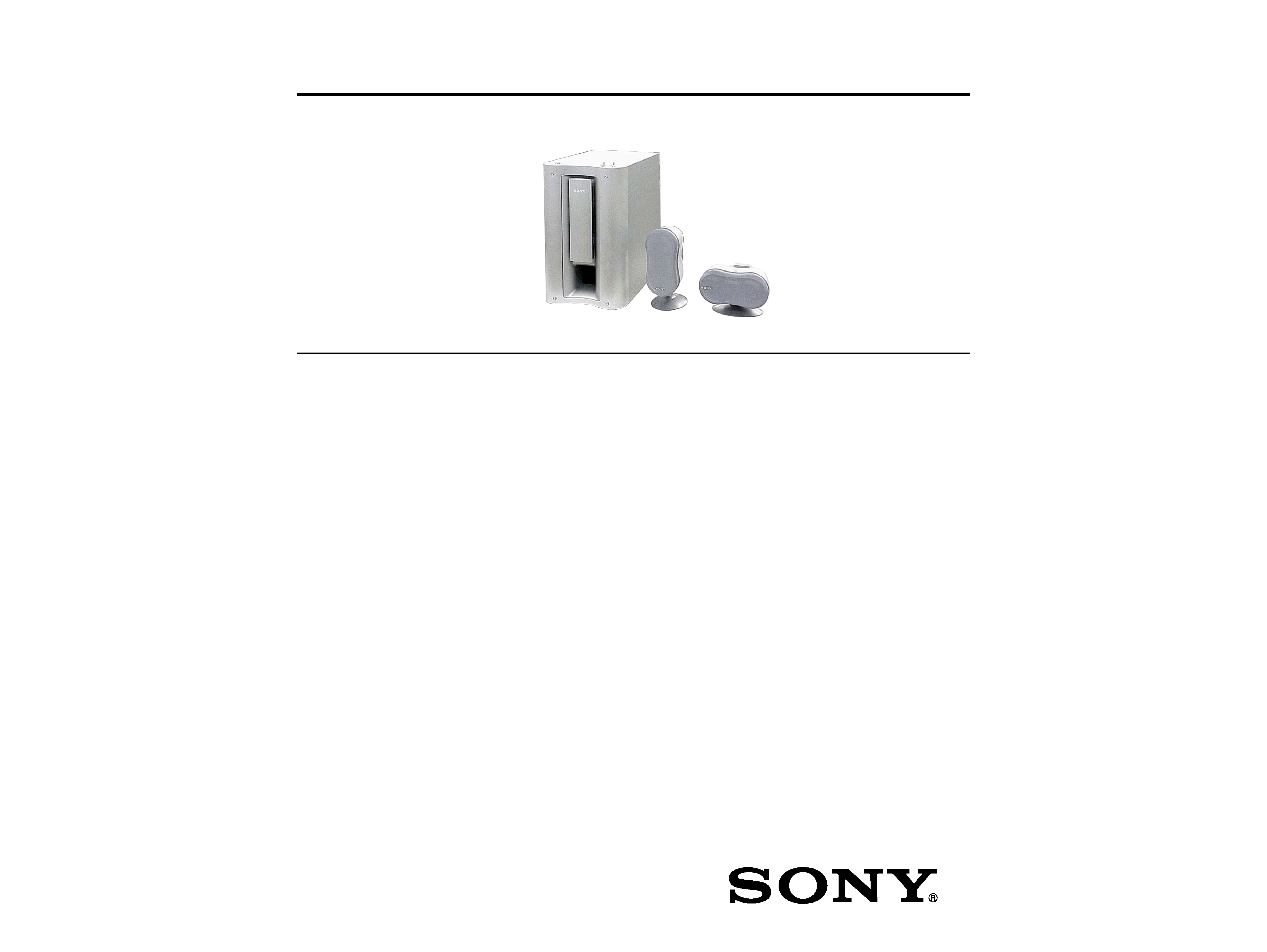
The SA-VE835ED system consists of one
unit of SA-WMS835 and five units of SS-
MS835.
Sony Corporation
Home Audio Company
Published by Sony Engineering Corporation
9-873-688-02
2002H0400-1
© 2002. 08
MICRO SATELLITE SYSTEM
SA-VE835ED/WMS835/
SS-MS835
SA-WMS835
SS-MS835
SS-MS835
(front and rear)
(center)
General
Power requirements
120 V AC, 60 Hz
(US, CND, MX model)
220 240 V AC, 50/60 Hz
(AEP, UK, SP, AR, KR
model)
Power consumptions
50 W
1 W (standby mode)
Dimensions (w/h/d)
Approx. 230
× 395 × 485
mm (9 1/8
× 15 5/8 ×
19 1/8 in.),
including front grille
Mass
Approx. 15.5 kg
(34 lb 3 oz)
Supplied accessories
Speaker stands (for the front and rear speakers) (4)
Speaker stand (for the center speaker) (1)
Screws (for the speaker stands) (5)
Washers (for the speaker stands) (5)
L-shaped Allen (Hex) Head wrench (1)
Speaker connecting cords, 10 m (32 ft 9 3/4 in.) (2)
Speaker connecting cords, 3.5 m (11 ft 6 in.) (3)
Audio connecting cord (1)
Design and specifications are subject to change
without notice.
·Abbreviation
CND : Canadian model
SP
: Singapore model
MX : Mexican model
AR
: Argentine model
KR
: Korean model
2
SA-VE835ED/WMS835/SS-MS835
TABLE OF CONTENTS
1. DIAGRAMS
1-1. Circuit Boards Location (SA-WMS835) ............................ 3
1-2. Printed Wiring Boards (SA-WMS835)
Audio Section .................................................................. 4
1-3. Printed Wiring Boards (SA-WMS835)
Main Power Section ........................................................ 5
1-4. Schematic Diagram (SA-WMS835) ................................... 6
2. EXPLODED VIEWS
2-1. Front Panel Section (SA-WMS835) .................................... 7
2-2. Rear Panel Section (SA-WMS835) ..................................... 8
2-3. Speaker Section (SS-MS835) .............................................. 9
3. ELECTRICAL PARTS LIST ........................................ 10
SAFETY-RELATED COMPONENT WARNING!!
COMPONENTS IDENTIFIED BY MARK 0 OR DOTTED LINE
WITH MARK 0 ON THE SCHEMATIC DIAGRAMS AND IN
THE PARTS LIST ARE CRITICAL TO SAFE OPERATION.
REPLACE THESE COMPONENTS WITH SONY PARTS WHOSE
PART NUMBERS APPEAR AS SHOWN IN THIS MANUAL OR
IN SUPPLEMENTS PUBLISHED BY SONY.
ATTENTION AU COMPOSANT AYANT RAPPORT
À LA SÉCURITÉ!!
LES COMPOSANTS IDENTIFIÉS PAR UNE MARQUE 0 SUR LES
DIAGRAMMES SCHÉMATIQUES ET LA LISTE DES PIÈCES
SONT CRITIQUES POUR LA SÉCURITÉ DE FONCTIONNEMENT.
NE REMPLACER CES COMPOSANTS QUE PAR DES PIÈCES
SONY DONT LES NUMÉROS SONT DONNÉS DANS CE MANUEL
OU DANS LES SUPPLÉMENTS PUBLIÉS PAR SONY.
To Exposed Metal
Parts on Set
0.15µF
1.5k
AC
voltmeter
(0.75V)
Earth Ground
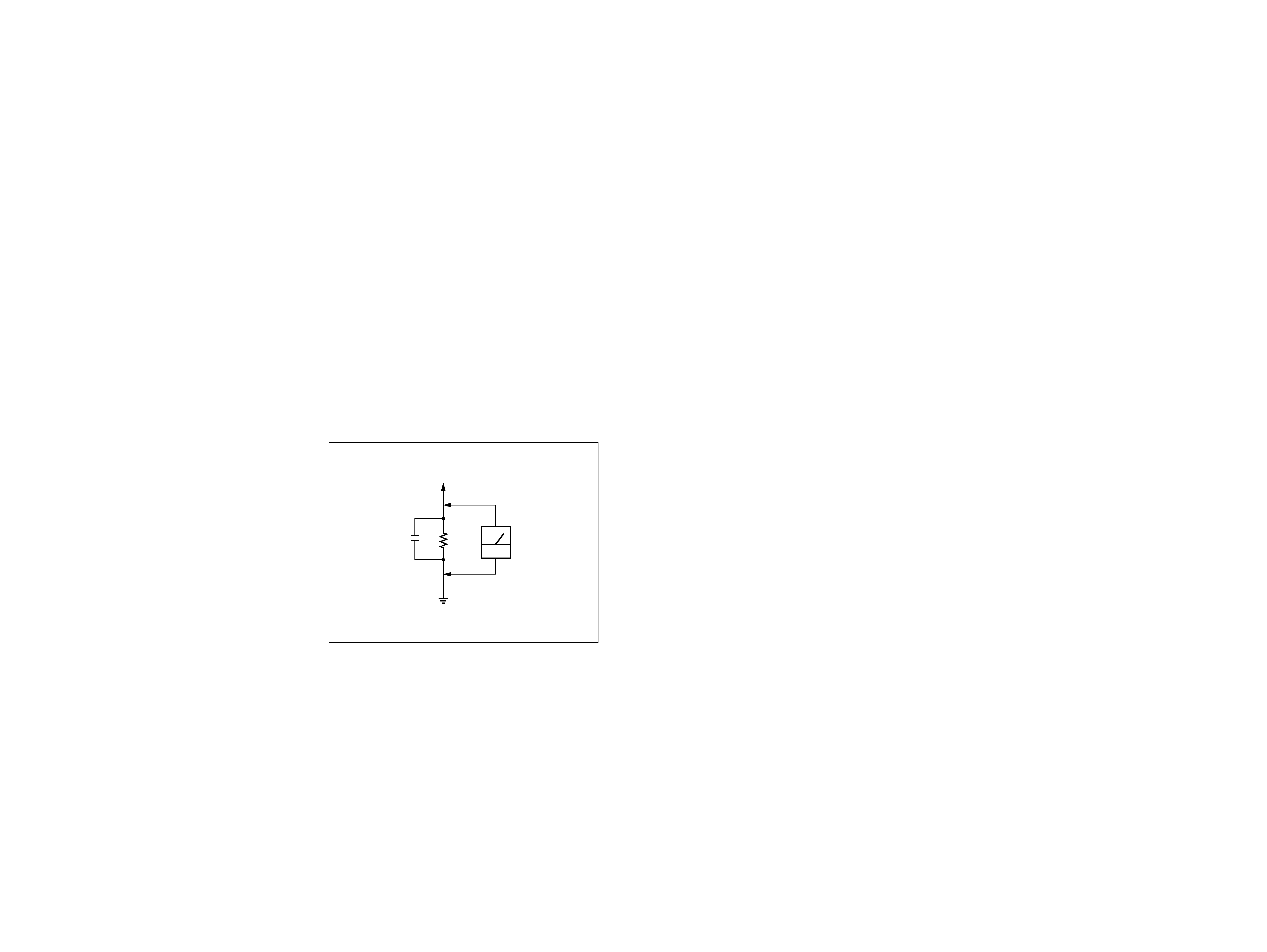
Fig. A. Using an AC voltmeter to check AC leakage.
SAFETY CHECK-OUT
After correcting the original service problem, perform the following
safety check before releasing the set to the customer:
Check the antenna terminals, metal trim, "metallized" knobs, screws,
and all other exposed metal parts for AC leakage. Check leakage as
described below.
LEAKAGE TEST
The AC leakage from any exposed metal part to earth ground and
from all exposed metal parts to any exposed metal part having a
return to chassis, must not exceed 0.5 mA (500 microamperes).
Leakage current can be measured by any one of three methods.
1. A commercial leakage tester, such as the Simpson 229 or RCA
WT-540A. Follow the manufacturers' instructions to use these
instruments.
2. A battery-operated AC milliammeter. The Data Precision 245
digital multimeter is suitable for this job.
3. Measuring the voltage drop across a resistor by means of a VOM
or battery-operated AC voltmeter. The "limit" indication is 0.75
V, so analog meters must have an accurate low-voltage scale. The
Simpson 250 and Sanwa SH-63Trd are examples of a passive
VOM that is suitable. Nearly all battery operated digital
multimeters that have a 2V AC range are suitable. (See Fig. A)
33
SA-VE835ED/WMS835/SS-MS835
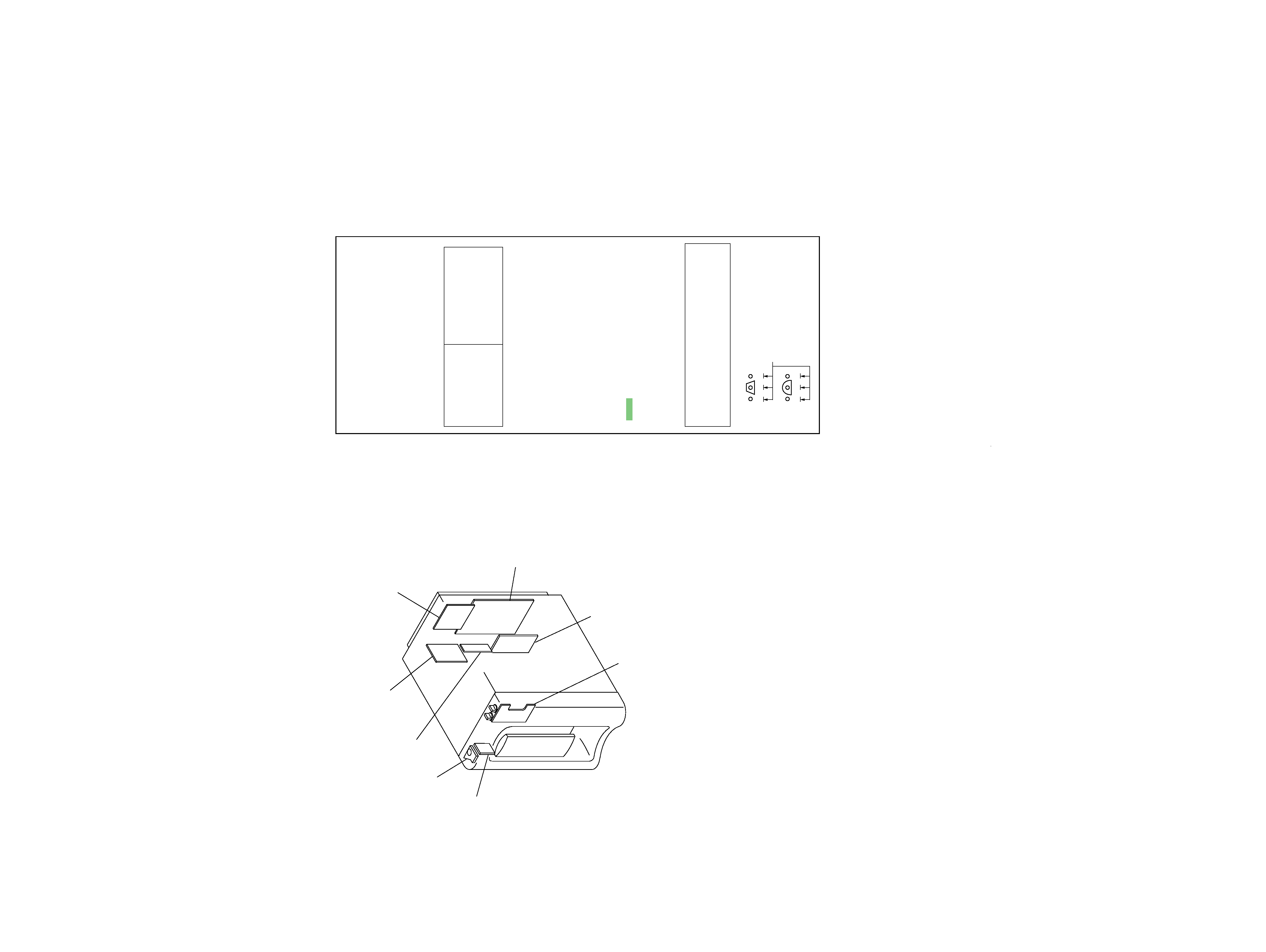
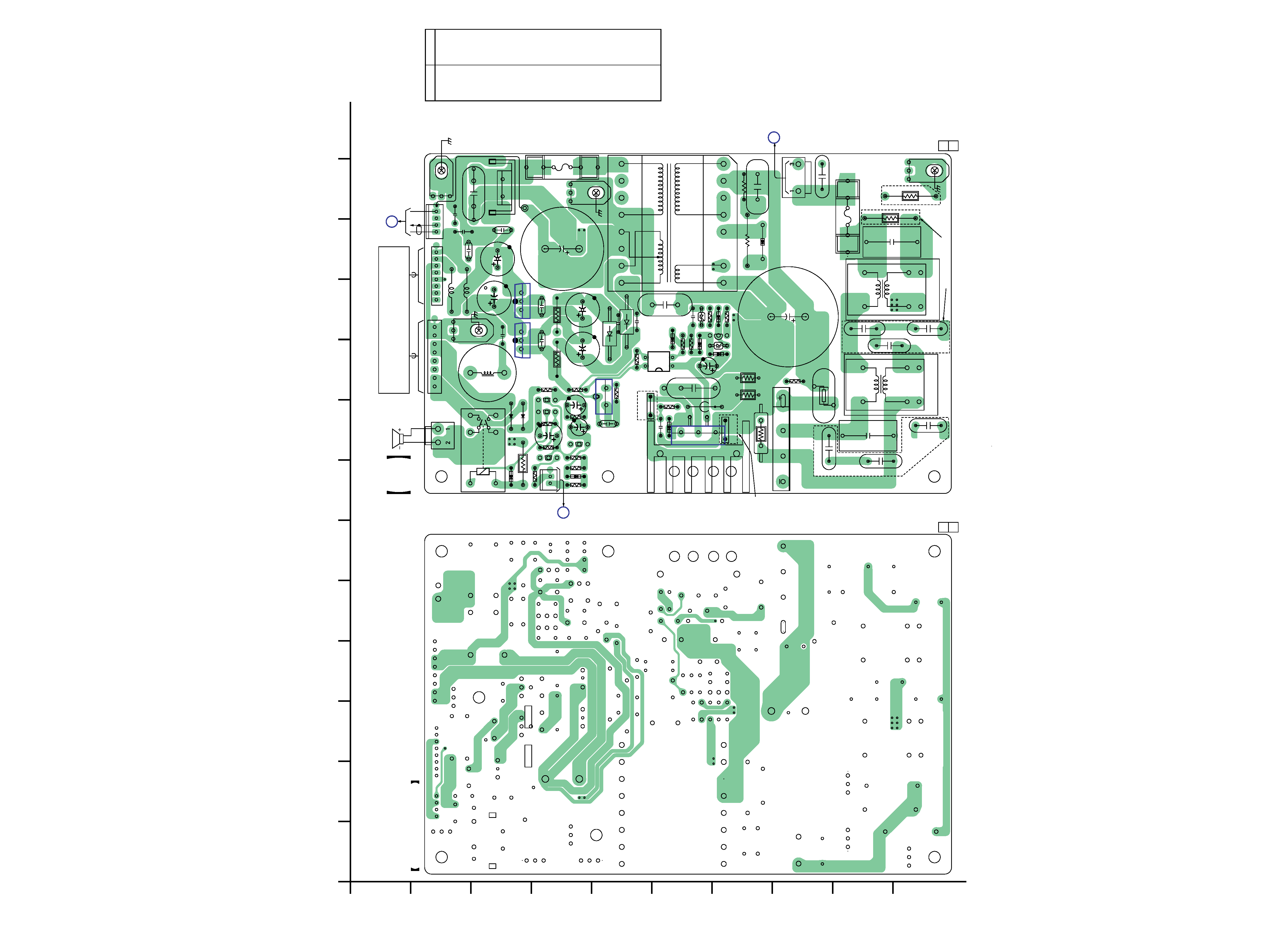
1-1. CIRCUIT BOARDS LOCATION (SA-WMS835)
SECTION 1
DIAGRAMS
MAIN POWER board
IC1
(power amplifier unit)
AUTO POWER board
CONTROL board
INPUT board
INPUT SELECT board
LED board
POWER SWITCH board
Note:
The components identi-
fied by mark 0 or dotted
line with mark 0 are criti-
cal for safety.
Replace only with part
number specified.
Note:
Les composants identifiés par
une marque 0 sont critiques
pour la sécurité.
Ne les remplacer que par une
piéce portant le numéro
spécifié.
THIS NOTE IS COMMON FOR PRINTED WIRING
BOARDS AND SCHEMATIC DIAGRAMS.
(In addition to this, the necessary note is
printed in each block.)
for schematic diagram:
· All capacitors are in µF unless otherwise noted. pF: µµF
50 WV or less are not indicated except for electrolytics
and tantalums.
· All resistors are in and 1/4 W or less unless otherwise
specified.
· 2 : nonflammable resistor.
· C : panel designation.
· A : B+ Line.
· B : B Line.
·Voltage is dc with respect to ground under no-signal
(detuned) condition.
·Voltages are taken with a VOM (Input impedance 10 M).
Voltage variations may be noted due to normal produc-
tion tolerances.
· Signal path.
F
: AUDIO
· Abbreviation
CND : Canadian model.
SP
: Singapore model.
for printed wiring boards:
· X : parts extracted from the component side.
·
: Pattern from the side which enables seeing.
· Abbreviation
CND : Canadian model.
SP
: Singapore model.
MX
: Mexican model.
AR
: Argentine model.
KR
: korean model.
Caution:
Pattern face side: Parts on the pattern face side seen from the
(Side B)
pattern face are indicated.
Parts face side: Parts on the parts face side seen from the
(Side A)
parts face are indicated.
B
These are omitted.
C
Q
Q
E
BC
E
Ver 1.1
4
4
SA-VE835ED/WMS835/SS-MS835
1
A
B
C
D
E
F
G
H
I
23456789
10
11
12
13
14
IC101
85
14
1-684-602-
(12)
12
1-684-601-
(12)
11
1-684-636-
(11)
11
1-684-636-
(11)
11
1-684-637- (11)
11
1-684-604- (12)
11
1-684-603-
(12)
11
1
3
2
VR301
C102
R101
R107
R106
R102
R103
C105
R105
JW2
JW3
JW4
R104
R108
R315
R317
JW8
CN301
R314
C307
R309
C310
C306
C305
JW21
C308
R313
JW20
C314
C316
JW17
R301
JW25
C1
S801
CN801
BLU
BLU
BRN
BRN
JW19
R402
D402
JW18
JW16
R310
R312
R318
R316
C309
C315
C317
JW7
JW26
C303
R308
C304
R307
R325
R326
C312
C313
C318
R327
C311
R311
MODE
MOVIE
MUSIC
LEVEL
POWER SAVE
AUTO
OFF
PHASE
REVERSE
NORMAL
ON/STANDBY
POWER
C106
JW24
D101
D102
MAIN
POWER
BOARD
CN906
MAIN
POWER
BOARD
CN909
MAIN POWER BOARD
CN901
C103
(CHASSIS)
J101
LINE
IN
C107
C606
C605
R602
R603
R601
R110
R111
C108
JW11
JW12
C601
JW1
JW9
JW10
CN103
CN102
R606
R604
Q605
Q603
Q604
Q602
Q601
C602
R605
C104
R109
JW14
JW13
JW22
CN101
JW23
CN104
C604
C603
6
1
4
21
1
16
1
16
6
INPUT BOARD
CONTROL BOARD
LED BOARD
AUTO POWER BOARD
(SIDE B)
AUTO POWER BOARD (SIDE A)
INPUT SELECT BOARD
POWER SWITCH BOARD
IC303
85
14
IC302
85
1
5
1
4
IC301
85
14
1
81
6
12
1
~ AC IN
13
2
1
2
CN401
RY801
C3
D807
T201
D204
D201
D202
D203
C201
C202
R201
C203
D205
Q201
C205
R202
C204
D206
Q202
C206
D207
D208
D209
D210
D211
R203
R204
R205
R206
R207
R208 R209
R210
R211
R212
R213
R214
IC201
Q203
Q205
Q206
Q207
Q204
C207
C208
CN210
CN203
CN212
CN202
CN204
CN211
SW502
SW501
CN501
3
1
SW301
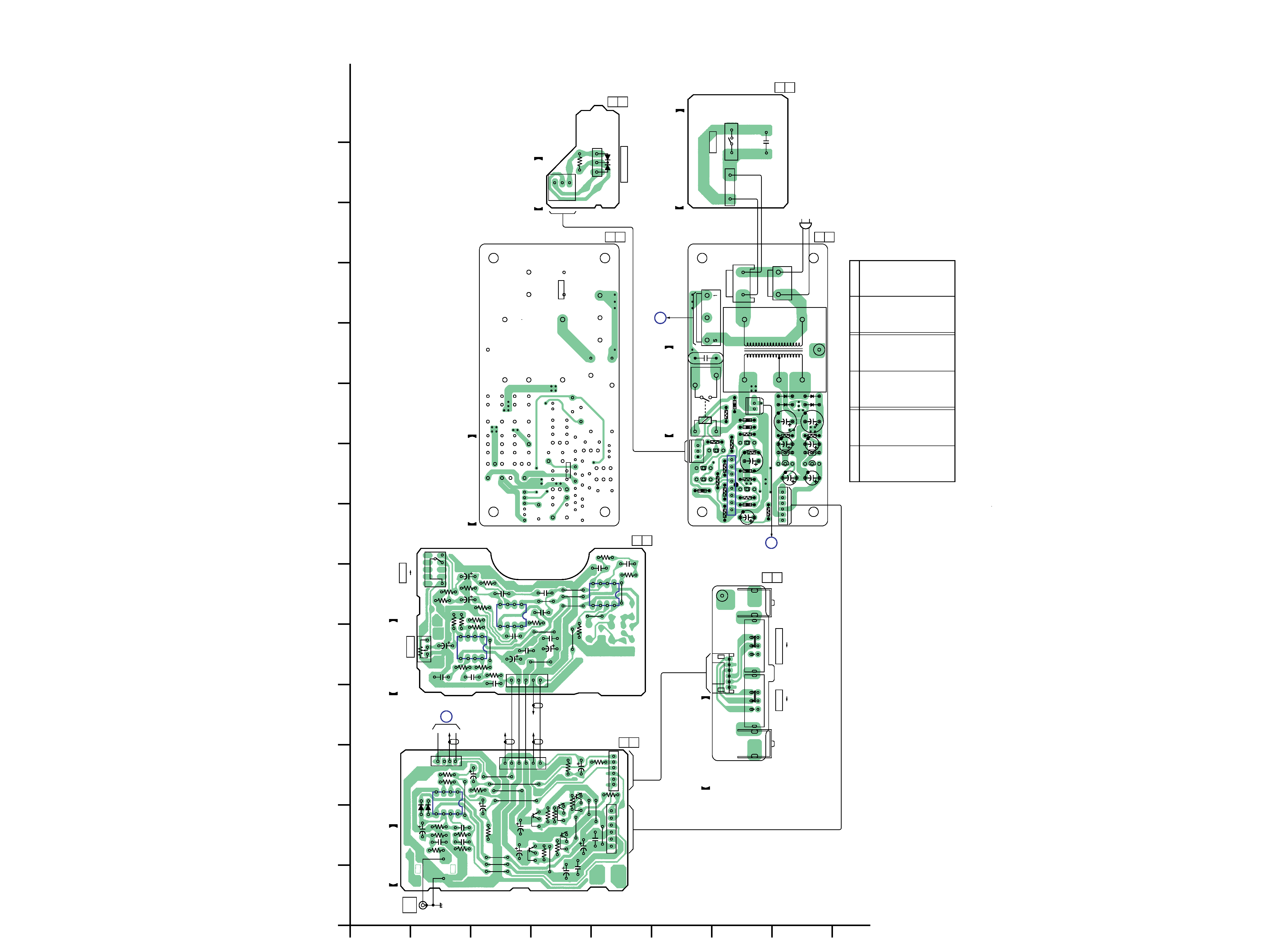
1-2. PRINTED WIRING BOARDS (SA-WMS835) -- AUDIO SECTION -- · Refer to page 3 for Circuit Boards Location.
Ref. No.
Location
D101
B-3
D102
B-3
D201
H-9
D202
H-9
D203
H-9
D204
H-9
D205
H-8
D206
H-8
D207
G-7
D208
G-8
D209
G-9
D210
G-9
· Semiconductor Location
D211
G-8
D402
E-13
D807
G-9
IC101
B-3
IC201
G-8
IC301
E-6
IC302
C-6
IC303
C-5
Q201
H-8
Q202
H-8
Q203
G-8
Q204
G-8
Q205
F-8
Q206
F-8
Q207
G-8
Q601
D-3
Q602
D-2
Q603
D-2
Q604
D-2
Q605
D-2
Ref. No.
Location
Ref. No.
Location
(Page 5)
(Page 5)
(Page 5)
55
SA-VE835ED/WMS835/SS-MS835
1-3. PRINTED WIRING BOARDS (SA-WMS835) -- MAIN POWER SECTION -- · Refer to page 3 for Circuit Boards Location.
1
A
B
C
D
E
F
G
H
I
J
23456789
10
11
12
13
1-684-635-
(11)
11
1-684-635-
(11)
11
2
1
3
AUTO
POWER
BOARD
CN211
AUTO
POWER
BOARD
CN202
INPUT BOARD
CN104
1
1
1
2
4
3
1
3
5
2
4
2
3
31
14
18
1
SP1
SPEAKER
BLK
RED
8
3
22
MAIN POWER BOARD (SIDE A)
MAIN
POWER
BOARD
IC1
POWER AMPLIFIER
UNIT
(ICE250A)
(CHASSIS)
(CHASSIS)
(CHASSIS)
(CHASSIS)
(SIDE B)
F901
T901
D901
IC901
C910
C911
R902
C902
C903
R901
R906
D902
C912
EP901
C908
C915
D903
R912
D908
Q901
R909
D907
C913
R907
D906
D904
D905
R905
R916
R913
R915
R908
R910
R911
THP901
R904
C901
C914
FB901
D922
FH901
FH902
R903
L902
C904
C916
C905
JW901
JW902
AEP,UK,SP,AR,KR MODEL
US,CND,MX
MODEL
US,CND,MX
MODEL
US,CND,MX MODEL
AEP,UK,SP,AR,KR MODEL
C2
RY701
C920
C919
L904
L905
D909
C922
R914
IC906
IC907
C934
C935
C936
C937
C932
C933
D701
R706
C703
Q704
R705
C702
R703
R704
Q703
C701
Q701
R702
D919
D920
C917
L903
R707
D911
D910
IC902
FH903
FH904
F902
CN904
CN907
R917
R918
R708
CN906
C918
CN912
EP903
C939
C938
PC901
C940
C941
C942
EP904
EP902
R701
1
2
CN909
D921
C906
C907
L901
CN903
CN901
Q705
R709
~~
FC1
FC1
KA
Ref. No.
Location
D701
D-7
D901
H-8
D902
G-11
D903
G-9
D904
G-9
D905
F-10
D906
G-10
D907
F-9
D908
F-9
D909
C-12
D910
E-10
D911
E-10
D919
C-8
D920
C-8
D921
C-7
D922
F-8
IC901
F-8
IC902
E-8
IC906
C-9
IC907
C-10
PC901
F-9
Q701
D-8
Q703
D-8
Q704
D-8
Q705
D-7
Q901
G-9
· Semiconductor
Location
(Page 4)
(Page 4)
(Page 4)
Ver 1.1