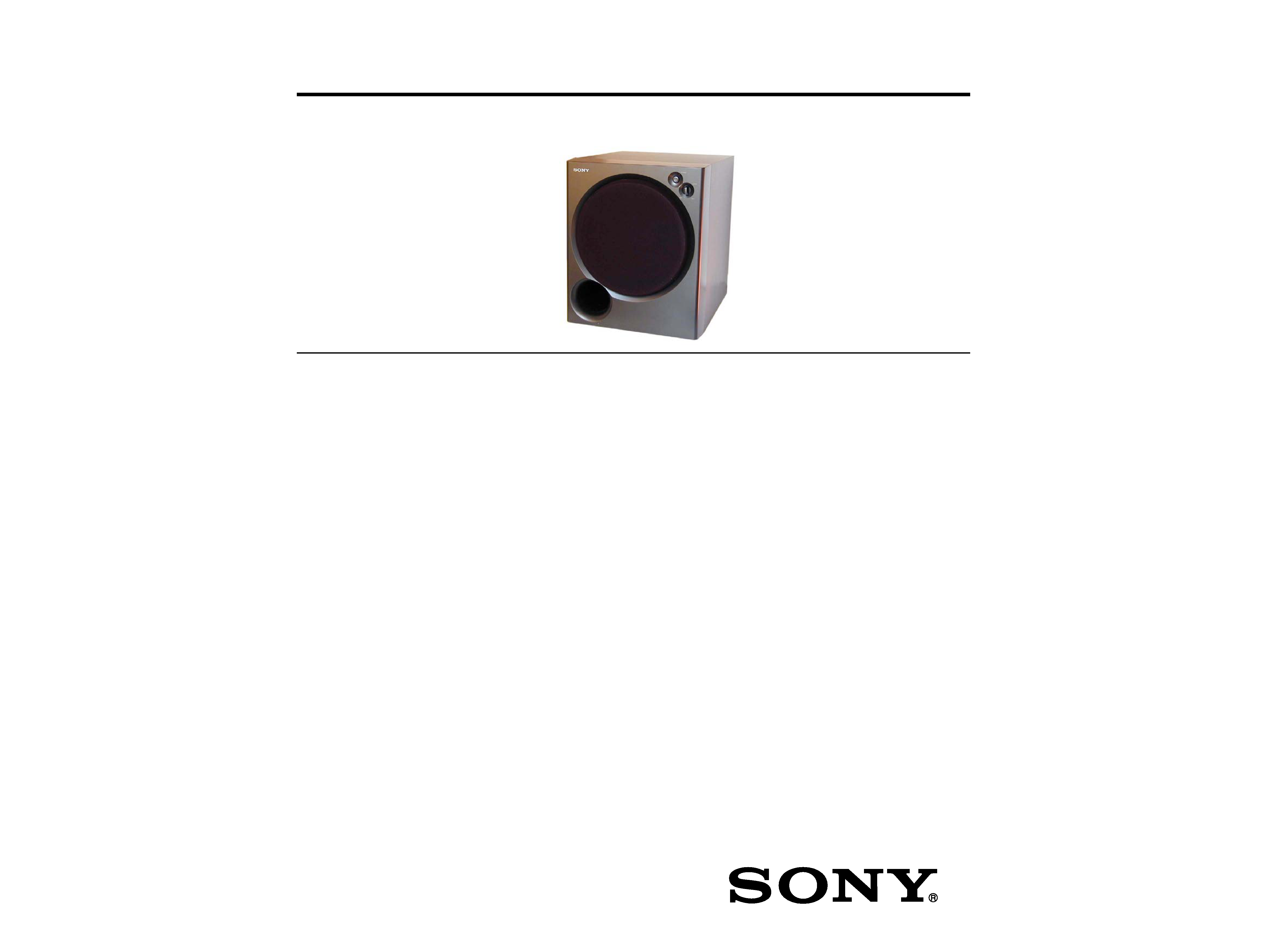
SA-WM200
SERVICE MANUAL
SPECIFICATIONS
US Model
Canadian Model
AEP Model
UK Model
E Model
9-877-108-02
2004G02-1
© 2004.07
Sony Corporation
Home Audio Company
Published by Sony Engineering Corporation
ACTIVE SUBWOOFER
Ver 1.1 2004.07
AUDIO POWER SPECIFICATIONS
POWER OUTPUT AND TOTAL HARMONIC
DISTORTION:
With 6 ohm loads, from 28 200 Hz; rated 80 watts, minimum RMS
power, with no more than 0.8 % total harmonic distortion from 250
milliwatts to rated output.
System
Type
Active Subwoofer (magnetically shielded design)
Speaker unit
Woofer: 20 cm dia. (8 in.), cone type
Amplifier section
Continuous RMS output : (0.8%) 80W
Reproduction frequency range
28 Hz 200 Hz
High frequency cut-off frequency
50 Hz 200 Hz
Phase selector
NORMAL, REVERSE
Inputs
Input jacks
INPUT: input pin jack
SPEAKER IN: input terminals
Output jacks
SPEAKER OUT: output terminals
General
Power requirements
USA and Canada models: 120 V AC, 60 Hz
Other models: 220-230V AC, 50/60 Hz
Power consumption
100 W
Dimensions
Approx. 270 x 325 x 398 mm
(10 3/4 x 12 7/8 x 15 11/16 in.) (w/h/d)
Mass
10 kg (22 lb 1oz)
Supplied accessories
Foot pads (4)
Audio connecting cord (1 phono 1 phono),
2 m (6 ft 6 1/2 in.) (1)
Speaker cords, 2.5 m (8 ft 2 1/2 in.) (2)
Design and specifications are subject to change without notice.
2
SA-WM200
Specifications ........................................................................... 1
1. GENERAL ...................................................................... 3
2. DIAGRAMS
2-1. Circuit Boards Location ............................................. 3
2-2. Printed Wiring Boards Main Section .................... 4
2-3. Printed Wiring Boards Input Control Section ....... 5
2-4. Printed Wiring Boards Power Section .................. 6
2-5. Schematic Diagram Main Section (1/2) ............... 7
2-6. Schematic Diagram Main Section (2/2) ............... 8
3. EXPLODED VIEWS
3-1. Main Section ............................................................... 9
4. ELECTRICAL PARTS LIST ................................... 10
TABLE OF CONTENTS
SAFETY CHECK-OUT
(US model)
After correcting the original service problem, perform the
following safety checks before releasing the set to the customer:
Check the antenna terminals, metal trim, "metallized" knobs,
screws, and all other exposed metal parts for AC leakage. Check
leakage as described below.
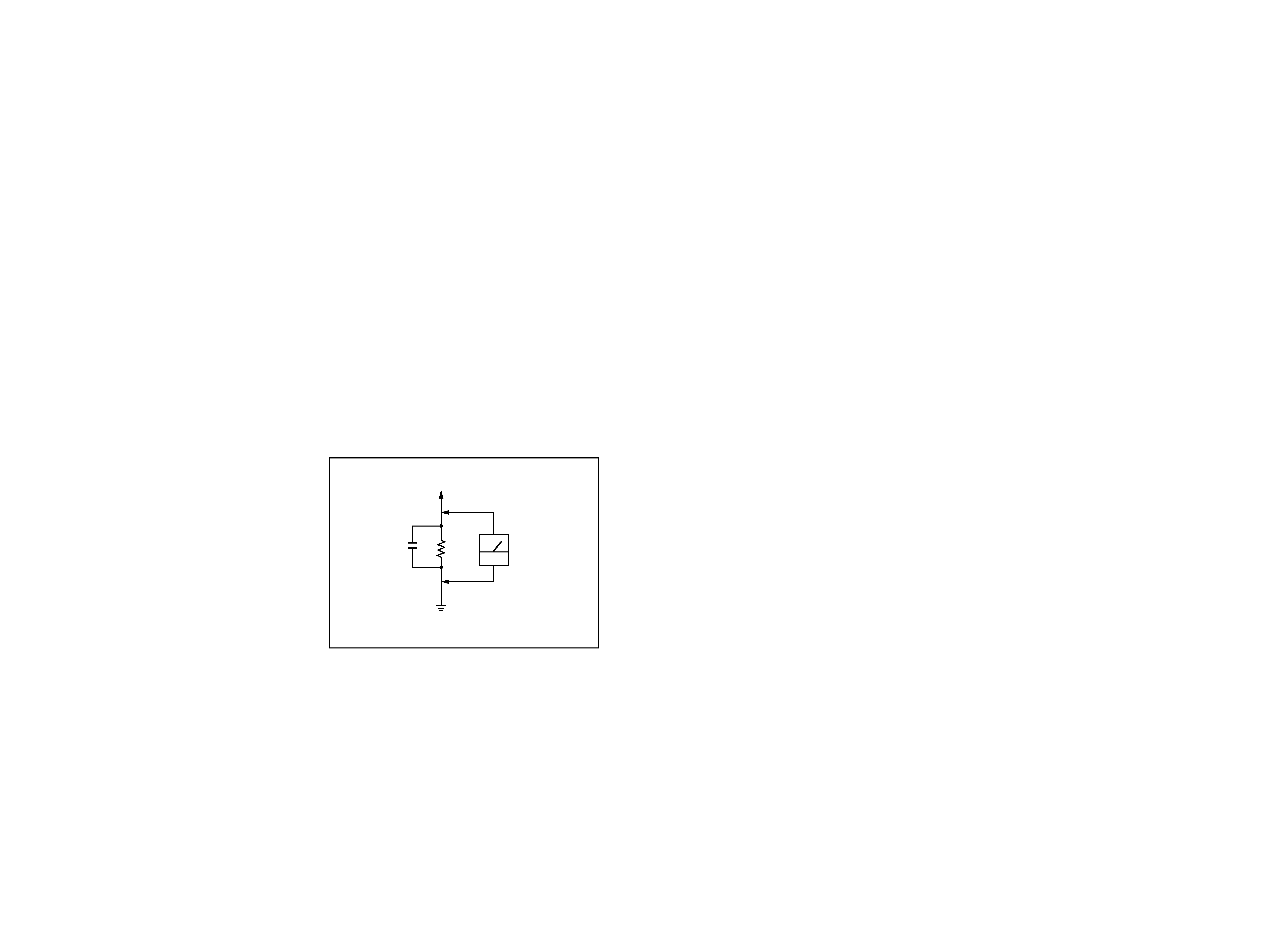
LEAKAGE
The AC leakage from any exposed metal part to earth Ground
and from all exposed metal parts to any exposed metal part
having a return to chassis, must not exceed 0.5 mA (500
microampers). Leakage current can be measured by any one of
three methods.
1. A commercial leakage tester, such as the Simpson 229 or
RCA WT-540A. Follow the manufacturers' instructions to
use these instruments.
2. A battery-operated AC milliammeter. The Data Precision
245 digital multimeter is suitable for this job.
3. Measuring the voltage drop across a resistor by means of a
VOM or battery-operated AC voltmeter. The "limit"
indication is 0.75 V, so analog meters must have an accurate
low-voltage scale. The Simpson 250 and Sanwa SH-63Trd
are examples of a passive VOM that is suitable. Nearly all
battery operated digital multimeters that have a 2V AC range
are suitable. (See Fig. A)
Fig. A. Using an AC voltmeter to check AC leakage.
0.15µF
To Exposed Metal
Parts on Set
1.5k
AC
voltmeter
(0.75V)
Earth Ground
SAFETY-RELATED COMPONENT WARNING!!
COMPONENTS IDENTIFIED BY MARK 0 OR DOTTED
LINE WITH MARK 0 ON THE SCHEMATIC DIAGRAMS
AND IN THE PARTS LIST ARE CRITICAL TO SAFE
OPERATION. REPLACE THESE COMPONENTS WITH
SONY PARTS WHOSE PART NUMBERS APPEAR AS
SHOWN IN THIS MANUAL OR IN SUPPLEMENTS PUB-
LISHED BY SONY.
ATTENTION AU COMPOSANT AYANT RAPPORT
À LA SÉCURITÉ!!
LES COMPOSANTS IDENTIFIÉS PAR UNE MARQUE 0 SUR
LES DIAGRAMMES SCHÉMATIQUES ET LA LISTE DES
PIÈCES SONT CRITIQUES POUR LA SÉCURITÉ DE
FONCTIONNEMENT. NE REMPLACER CES COMPOSANTS
QUE PAR DES PIÈCES SONY DONT LES NUMÉROS SONT
DONNÉS DANS CE MANUEL OU DANS LES SUPPLÉMENTS
PUBLIÉS PAR SONY.
3
3
SA-WM200
SECTION 1
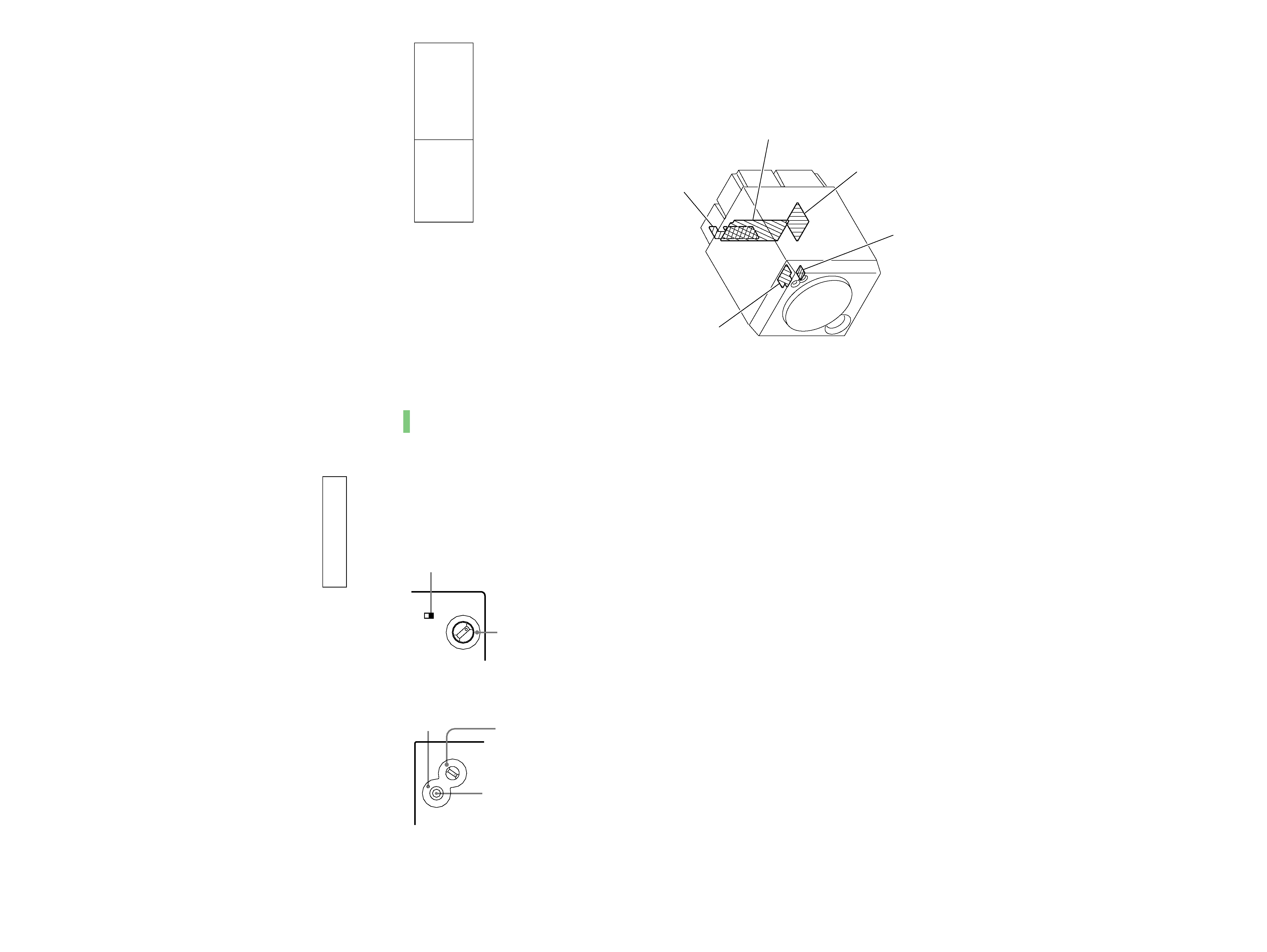
GENERAL
This section is extracted from
instruction manual.
LEVEL
PHASE
POWER
POWER indicator
CUT OFF FREQ
CUT OFF FREQ
200H z
NORMAL
REVERS E
50H z
PHASE
POWER
LEVEL
MIN
MAX
FRONT VIEW
REAR VIEW
· Location of controls
SECTION 2
DIAGRAMS
For Schematic Diagrams.
Note:
· All capacitors are in µF unless otherwise noted. pF: µµF 50 WV or
less are not indicated except for electrolytics and tantalums.
· All resistors are in and
1/4 W or less unless otherwise specified.
· C : panel designation.
THIS NOTE IS COMMON FOR PRINTED WIRING BOARDS AND SCHEMATIC DIAGRAMS.
(In addition to this, the necessary note is printed in each block.)
For Printed Wiring Boards.
Note :
· X : parts extracted from the component side.
· x : parts extracted from the conductor side.
·
: Pattern from the side which enables seeing.
· Abbreviation
CND : Canadian model
MY
: Malaysia model
SP
: Singapore model
· A : B+ Line.
· B : B Line.
·Voltages are dc with respect to ground under no-signal conditions.
· no mark : Power on
·Voltages are taken with a VOM (Input impedance 10 M).
Voltage variations may be noted due to normal production tolerances.
· Signal path.
F
: AUDIO
· Abbreviation
CND : Canadian model
MY
: Malaysia model
SP
: Singapore model
Note:
The components identi-
fied by mark 0 or dotted
line with mark 0 are criti-
cal for safety.
Replace only with part
number specified.
Note:
Les composants identifiés par
une marque 0 sont critiques
pour la sécurité.
Ne les remplacer que par une
piéce portant le numéro
spécifié.
2-1. CIRCUIT BOARDS LOCATION
SWITCH board
INPUT CONTROL board
MAIN board
POWER TRANS board
CONTROL board
4
4
SA-WM200
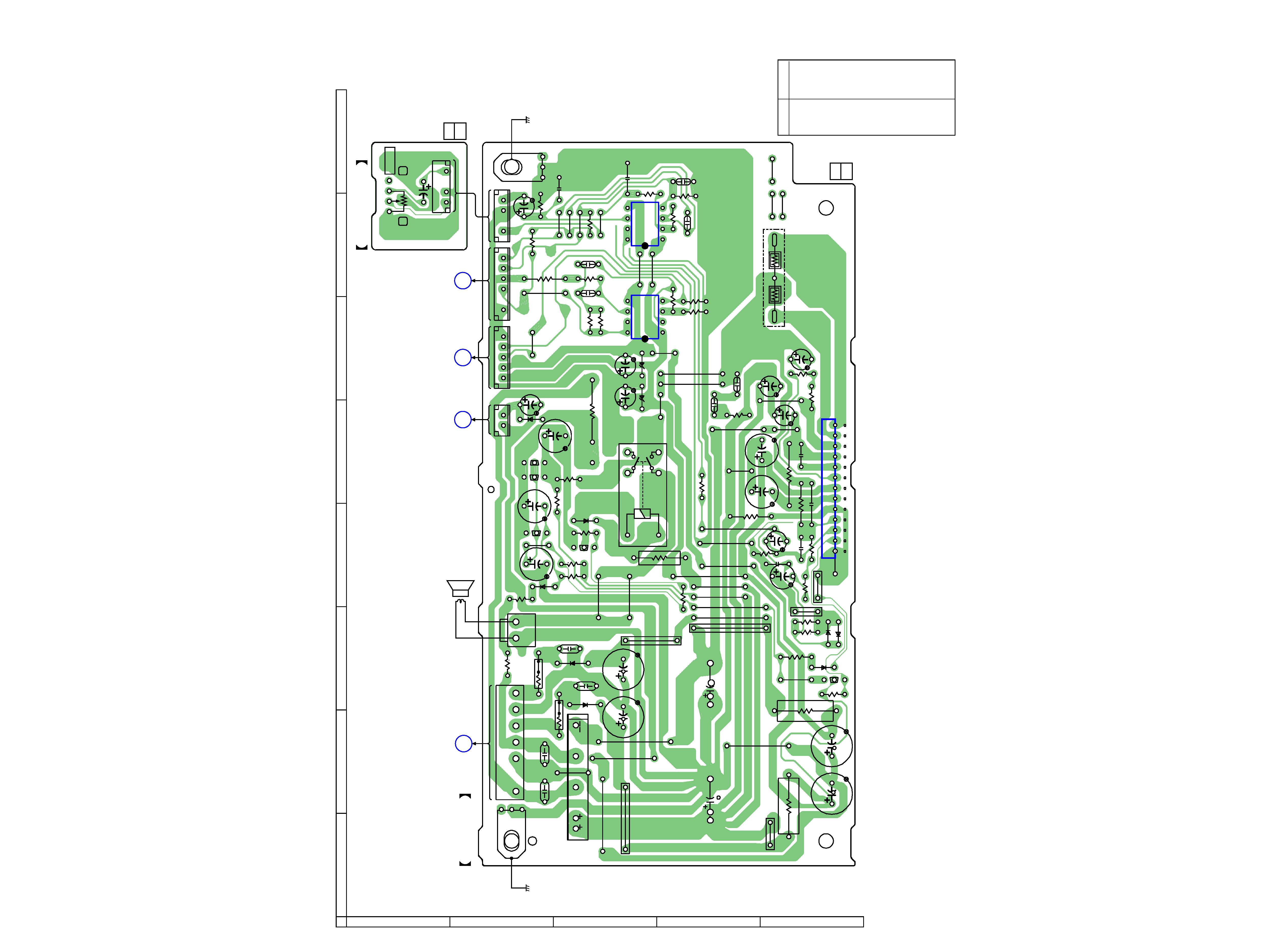
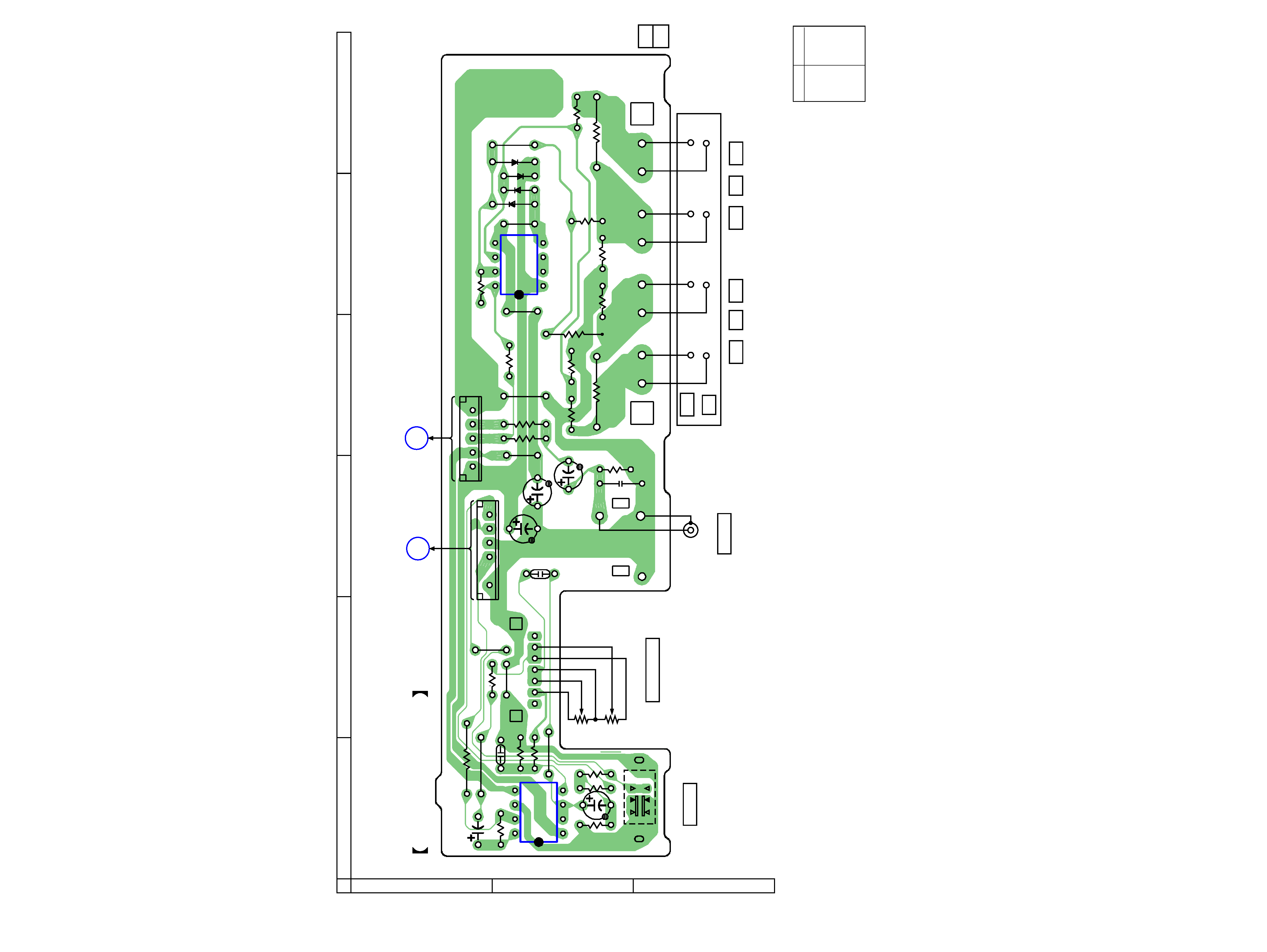
2-2. PRINTED WIRING BOARDS MAIN Section
CN402
CN301
CN204
IC301
RY301
C401
C402
C405
C407
C408
D402
D403
Q501
Q502
Q503
Q504
D501
C501
C502
E
E
C503
R403
R404
C308
C306
C307
R307
C302
R301
R302
R401
R402
D304
R311
R312
C309
C310
R502
R503
JW102
JW116
JW402
C303
JW114
JW115
R308
D401
D301
JW106
R309
R303
C301
JW301
R508
Q505
R506
D502
R507
JW401
JW124
JW126
JW127
JW501
C312
R505
R304
R501
G1
G2
JW112
R500
C409
C410
C313
JW128
R313
R315
D302
C406
R207
C203
C204
R208
R209
R210
R205
R212
R213
C208
R215
R216
C210
R217
C207
R214
C305
C304
R504
C601
D602
R601
D205
D206
C205
C206
JW123
JW105
CNP801
C801
IC203
IC202
JW107
CN201
JW108
JW132
JW109
R305
C311
CN202
JW125
JW110
R314
JW111
JW129
R306
JW101
CNP111
RV801
C404
JW404
JW403
JW103
JW104
C211
C209
JW117
JW118
R211
JW120
JW121
JW130
JW131
JW122
JW133
JW134
JW119
R206
R310
C403
JW135
11
(11)
1-686-982-
CONTROL BOARD
11
(11)
1-686-983-
MAIN BOARD
1
1
1
1
1
1
1
6
6
2
2
3
3
5
(CHASSIS)
(CHASSIS)
LEVEL
C
B
D
A
INPUT
CONTROL
BOARD
(Page 5)
INPUT
CONTROL
BOARD
(Page 5)
SWITCH
BOARD
(Page 6)
POWER
BOARD
(Page 6)
SP901
SPEAKER
1
13
1
4
5
8
1
4
5
8
E
E
E
2
3
4
5
6
7
8
A
1
B
C
D
E
z
See page 3 for Notes.
z
See page 3 for Circuit Boards Location.
Ref. No.
Location
z
Semiconductor
Location
D205
C-6
D206
C-6
D301
E-3
D302
E-3
D304
C-4
D401
C-2
D402
C-3
D403
C-3
D501
B-4
D502
E-3
D602
B-5
IC202
C-6
IC203
C-7
IC301
E-5
Q501
B-4
Q502
C-4
Q503
B-5
Q504
B-5
Q505
E-3
5
5
SA-WM200
2-3. PRINTED WIRING BOARDS INPUT CONTROL Section
z
See page 3 for Notes.
z
See page 3 for Circuit Boards Location.
IC201
IC701
R105
R106
R104
D204
R203
C101
C201
R110
S701
S701
RV701
RV701
R702
R703
R705
R706
R707
R708
C701
C702
C703
C704
C705
C706
CN701
CN101
R107
R101
R108
R109
JW207
D203
JW208
J101
JW210
TM101
SPEAKER
R103
R102
R204
R704
R701
D202
D201
JW204
JW205
JW209
JW701
JW702
JW206
R202
R201
INPUT CONTROL BOARD
11
(11)
1-686-985-
INPUT
CUT OFF FREQ
PHASE
1
4
5
8
1
1
1
4
5
5
5
8
+
OUT
IN
LR
+
B
C
MAIN
BOARD
(Page 4)
MAIN
BOARD
(Page 4)
NORMAL
REVERSE
t
2
3
4
5
6
A
1
B
C
Ref. No.
Location
z
Semiconductor
Location
D201
B-6
D202
B-5
D203
B-5
D204
B-5
IC201
B-5
IC701
B-1