1
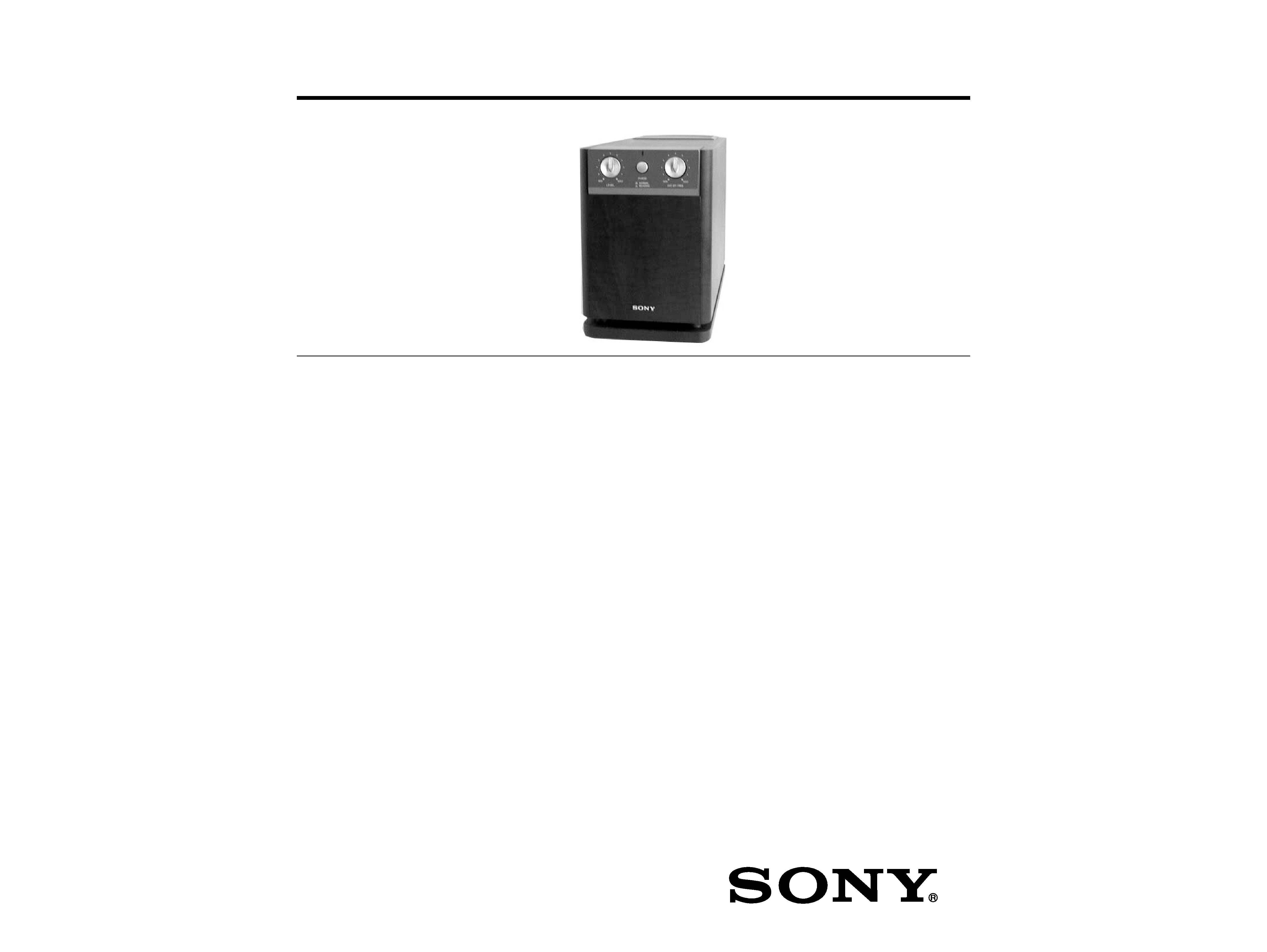
SA-WEX200
ACTIVE SUBWOOFER
US Model
Canadian Model
SPECIFICATION
Ver 1.0 2001.09
SA-WEX200 is sub woofer in CMT-EX200.
9-873-267-01
2001I0200-1
© 2001.9
Sony Corporation
Home Audio Company
Shinagawa Tec Service Manual Production Group
Amplifier section
For the U.S.model
AUDIO POWER SPECIFICATIONS
POWER OUTPUT AND TOTAL HARMONIC
DISTORTION:
With 4 ohms loads,from 50 150 Hz;rated 30 watts
per channel minimum RMS power,with no more than
10%total harmonic distortion from 250 milli watts to
rated output.
Canadian model:
Continuous RMS power output (reference):
30 watts
(4 ohms at 55 Hz,10%
THD)
Speaker system
Active sub woofer
(magnetically shielded
design)
Speaker unit
10 cm dia,cone type
woofer (x2)
Practical maximum output 30 watts
Reproduction frequency range
45 150 Hz
High frequency cut-off range
70 150 Hz
Phase selector
Normal,reverse
Input
SPEAKER INPUT:
Input terminal
Output
SPEAKER OUTPUT:
Output terminal
Power requirements
120 V AC,60 Hz
Power consumption
40 watts
Dimensions
Approx.150 x 220 x
345 mm (w/h/d,incl.
projecting parts and
controls)
Mass
Approx.6.2 kg
Design and specifications are subject to change
without notice.
SERVICE MANUAL
2
SA-WEX200
TABLE OF CONTENTS
1. GENERAL .......................................................................... 3
2. DIAGRAMS
2-1. Circuit Boards Location ........................................................ 3
2-2. Printed Wiring Board ............................................................ 4
2-3. Schematic Diagram ............................................................... 5
3. EXPLODED VIEW
3-1. Front Section ......................................................................... 6
4. ELECTRICAL PARTS LIST ......................................... 6
SAFETY-RELATED COMPONENT WARNING!!
COMPONENTS IDENTIFIED BY MARK 0 OR DOTTED LINE WITH
MARK 0 ON THE SCHEMATIC DIAGRAMS AND IN THE PARTS
LIST ARE CRITICAL TO SAFE OPERATION. REPLACE THESE
COMPONENTS WITH SONY PARTS WHOSE PART NUMBERS
APPEAR AS SHOWN IN THIS MANUAL OR IN SUPPLEMENTS
PUBLISHED BY SONY.
ATTENTION AU COMPOSANT AYANT RAPPORT
À LA SÉCURITÉ!
LES COMPOSANTS IDENTIFÉS PAR UNE MARQUE 0 SUR LES
DIAGRAMMES SCHÉMATIQUES ET LA LISTE DES PIÈCES SONT
CRITIQUES POUR LA SÉCURITÉ DE FONCTIONNEMENT. NE
REMPLACER CES COMPOSANTS QUE PAR DES PIÈSES SONY
DONT LES NUMÉROS SONT DONNÉS DANS CE MANUEL OU
DANS LES SUPPÉMENTS PUBLIÉS PAR SONY.
After correcting the original service problem, perform the
following safety checks before releasing the set to the customer:
Check the antenna terminals, metal trim, "metallized" knobs, screws,
and all other exposed metal parts for AC leakage. Check leakage as
described below.
LEAKAGE
The AC leakage from any exposed metal part to earth ground and
from all exposed metal parts to any exposed metal part having a
return to chassis, must not exceed 0.5 mA (500 microamperes).
Leakage current can be measured by any one of three methods.
1.
A commercial leakage tester, such as the Simpson 229 or RCA
WT-540A. Follow the manufacturers' instructions to use these
instruments.
2.
A battery-operated AC milliammeter. The Data Precision 245
digital multimeter is suitable for this job.
3.
Measuring the voltage drop across a resistor by means of a
VOM or battery-operated AC voltmeter. The "limit" indication
is 0.75 V, so analog meters must have an accurate low-voltage
scale. The Simpson 250 and Sanwa SH-63Trd are examples of
a passive VOM that is suitable. Nearly all battery operated
digital multimeters that have a 2V AC range are suitable. (See
Fig. A)
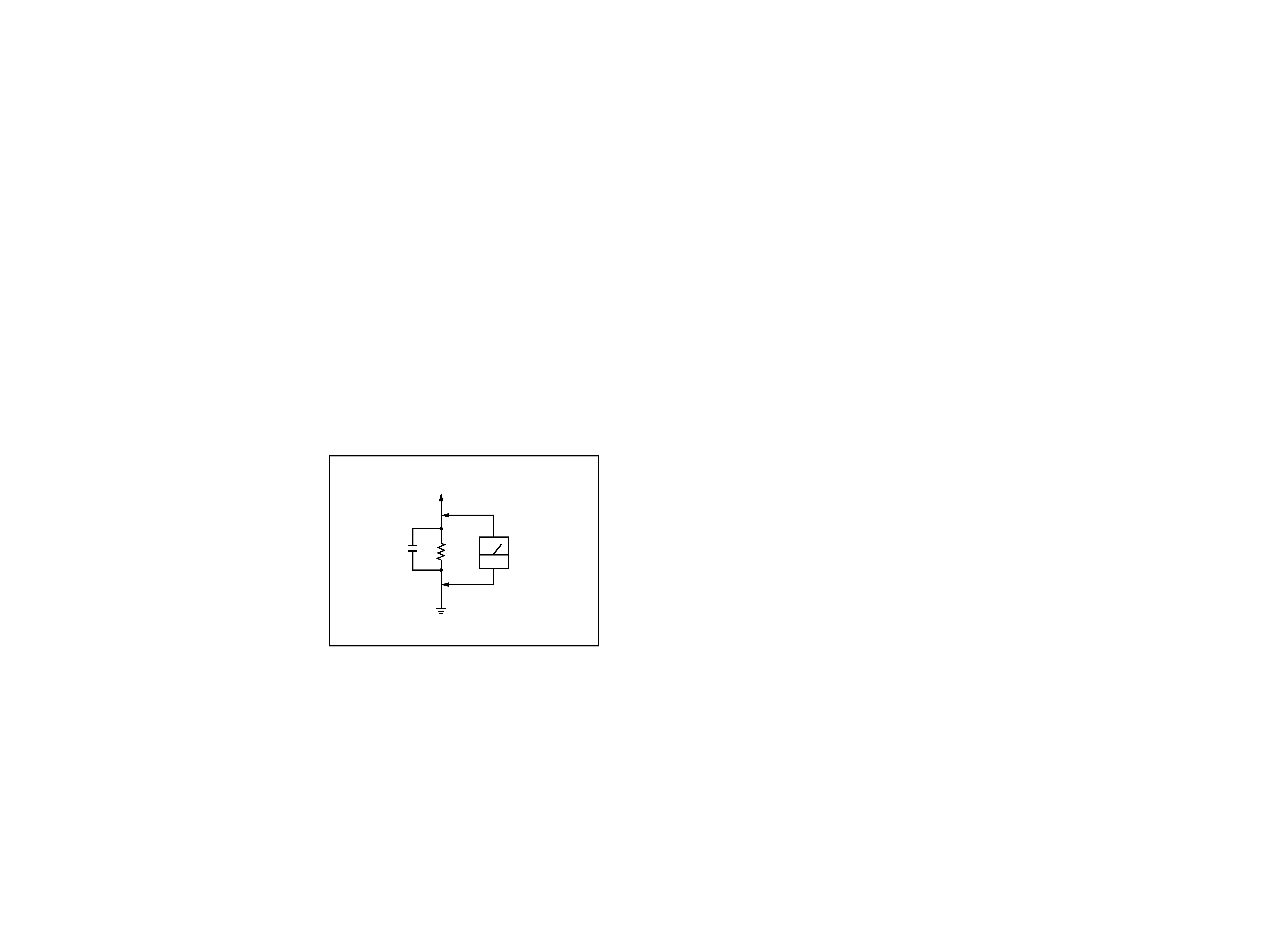
SAFETY CHECK-OUT
(US model)
Fig. A. Using an AC voltmeter to check AC leakage.
0.15
µF
To Exposed Metal
Parts on Set
1.5k
AC
voltmeter
(0.75V)
Earth Ground
33
SA-WEX200
SECTION 1
GENERAL
SECTION 2
DIAGRAMS
For schematic diagrams.
Note:
· All capacitors are in
µF unless otherwise noted. pF: µµF
50 WV or less are not indicated except for electrolytics
and tantalums.
· All resistors are in
and 1/4 W or less unless otherwise
specified.
· C : panel designation.
For printed wiring boards.
Note:
· X : parts extracted from the component side.
· b : Pattern from the side which enables seeing.
·
: B+ Line.
·
: B Line.
· Voltages are dc with respect to ground under no-signal con-
ditions.
no mark : Power on
· Voltages are taken with a VOM (Input impedance 10M
).
Voltage variations may be noted due to normal preduction
tolerances.
· Signal path.
K : AUDIO
THIS NOTE IS COMMON FOR PRINTED WIRING BOARDS AND
SCHEMATIC DIAGRAMS.
(In addition to this, the necessary note is printed in each block.)
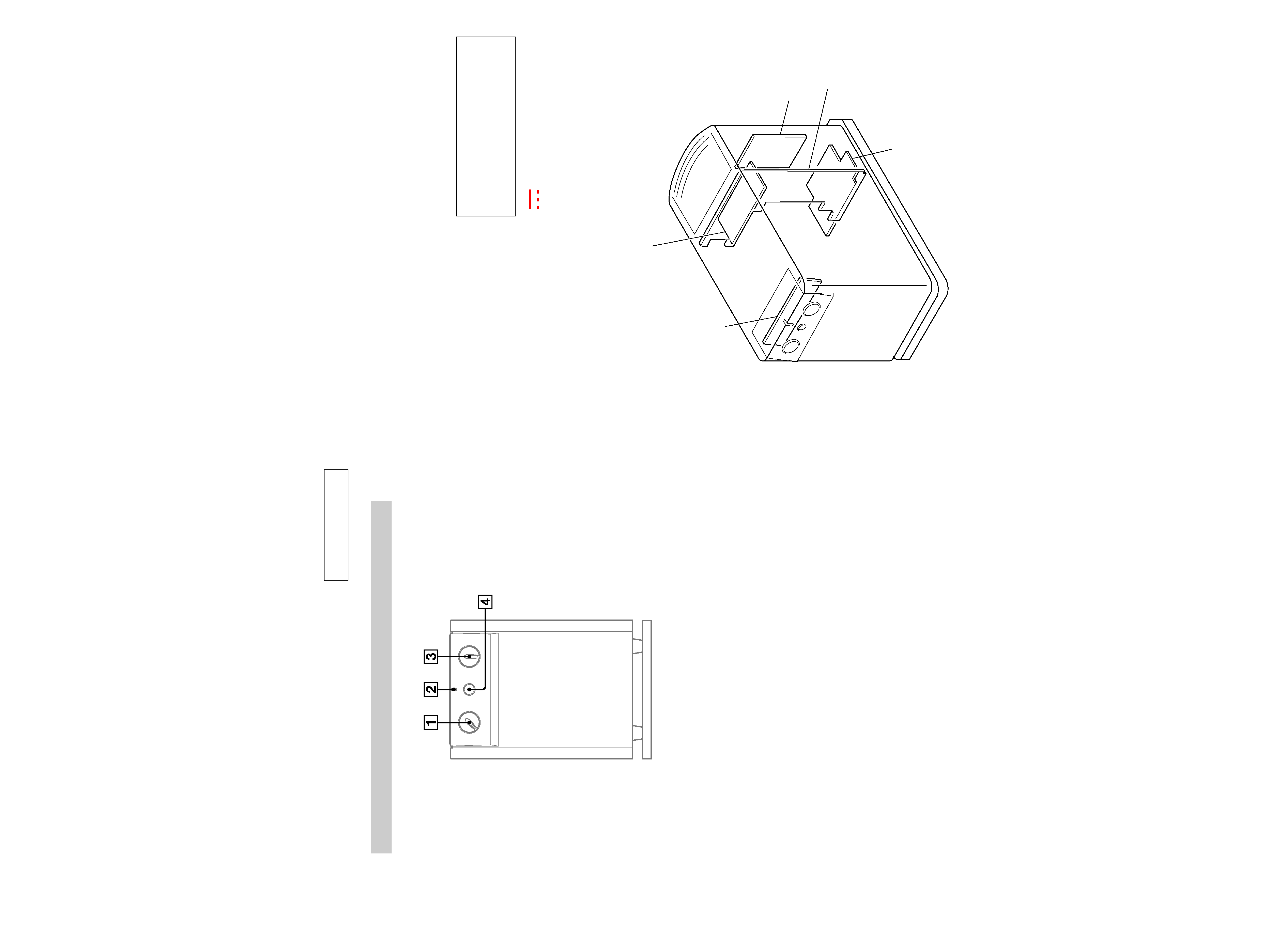
2-1. Circuit Boards Location
Note:
The components identi-
fied by mark 0 or dotted
line with mark 0 are criti-
cal for safety.
Replace only with part
number specified.
Note:
Les composants identifiés par
une marque 0 sont critiques
pour la sécurité.
Ne les remplacer que par une
piéce por tant le numéro
spécifié.
This section is extracted from
instruction manual.
Sub Woofer
CUT OFF FREQ 3 (15)
LEVEL 1 (15)
PHASE 4 (15)
Power indicator 2
· Location of controls
INPUT board
MAIN board
AC board
POWER AMP board
FRONT board
44
SA-WEX200
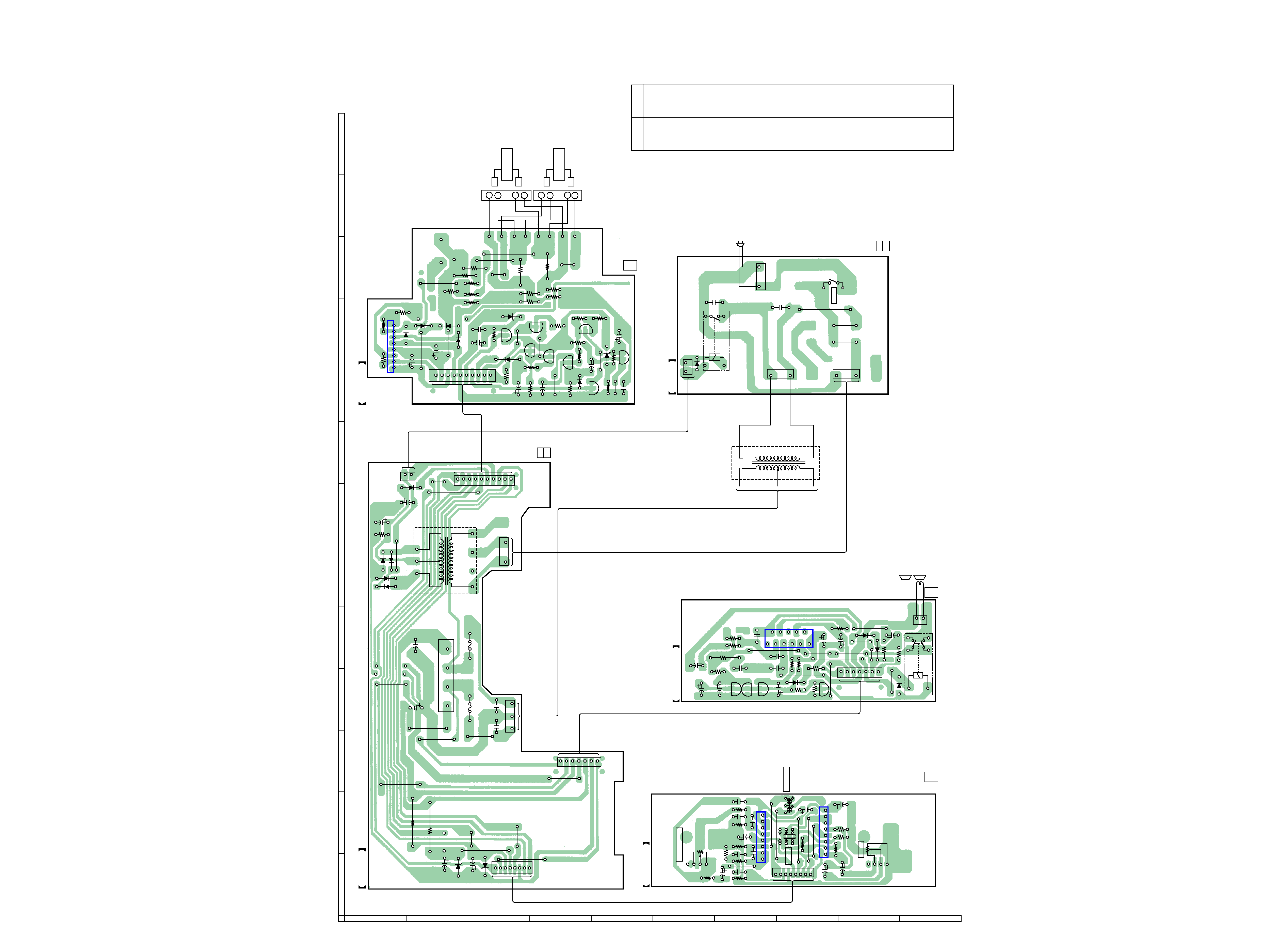
2-2. PRINTED WIRING BOARD
· See page 3 for Circuit Boards Location.
1
8
CN201
1
8
IC201
1
8
IC202
R204
R214
R117
R115
R203
R116
R114
R206
R207
R208
R205
C209
C208
C211
C210
C205
C207
C213
C203
C212
C204
C103
C104
D201
ON/STBY
RV202
LEVEL
RV201
CUT OFF FREQ
FRONT BOARD
11
(11)
S201
PHASE
1
11
10
2
L
SPEAKER
INPUT
R
TM101
+
+
L
SPEAKER
OUTPUT
R
+
+
1
8
1
2
1
2
1
2
3
1
2
R401
R402
C452
C451
C404
C406
C405
C403
C401
C402
1
8
CN201M
1
7
CN302W
1
3
CN501
1
10
CN301W
1
CN203M
1
CN502
T2
F402
+
F401
D401
D404
D403
D451
D455
D454
D453
D452
R451
MAIN BOARD
11
(11)
R303
R304
R309
R307
R310
R311
Q303
Q304
Q302
Q301
R313
R312
R301
R308
R302
B C E
E C B
E C B
E C B
C309
C305
C311
C306
C312
C310
C303
C302
C308
C307
C320
R306
C314
D302
D304
D303
1
7
CN302
1
CN303
RY301
D301
IC851
POWR AMP BOARD
11
(11)
SP901
SP902 (PASSIVE WOOFER)
INPUT BOARD
11
(11)
R503
R513
R501
R507
R120
R121
R502
R504
R511
R506
R103
R510
R512
R515
R514
R508
R509
R505
R105
R102
R101
R106
R112
R123
R122
R118
R111
IC101
R107
C505
C504
C704
C703
CN301
10
1
C506
C501
C503
C507
C502
C701
C711
D102
D503
D504
D103
D101
D104
D501
D502
D505
B
C
E
E C B
E C B
E C B
B C E
B C E
B C E
E
C
B
Q501
Q507
Q508
Q506
Q503
Q504
Q502
Q505
RY461
C2
C3
D461
1
CN203
CN503
CN501M
CN502M
S1
POWER
AC BOARD
11
(11)
CP901
AC IN
T1
POWER
TRANSFORMER
2
3
4
567
8
910
11
12
13
A
1
B
C
D
E
F
G
H
J
I
1-683-832-
1-683-834-
1-683-831-
1-683-833-
1-683-835-
D101
B-10
D102
B-10
D103
B-10
D104
A-10
D201
H-2
D301
I-5
D302
I-5
D303
I-4
D304
H-4
D401
B-4
D403
B-1
D404
C-1
D451
A-6
D452
A-6
D453
A-6
D454
A-6
D455
B-7
D461
F-9
D501
C-10
D502
E-10
D503
D-9
D504
C-10
IC101
A-10
IC201
G-2
IC202
H-2
IC851
H-5
Q301
G-4
Q302
G-4
Q303
H-4
Q304
G-4
Q501
C-10
Q502
E-10
Q503
D-9
Q504
D-10
Q505
E-9
Q506
D-10
Q507
D-10
Q508
C-10
· Semiconductor
Location
Ref. No.
Location
55
SA-WEX200
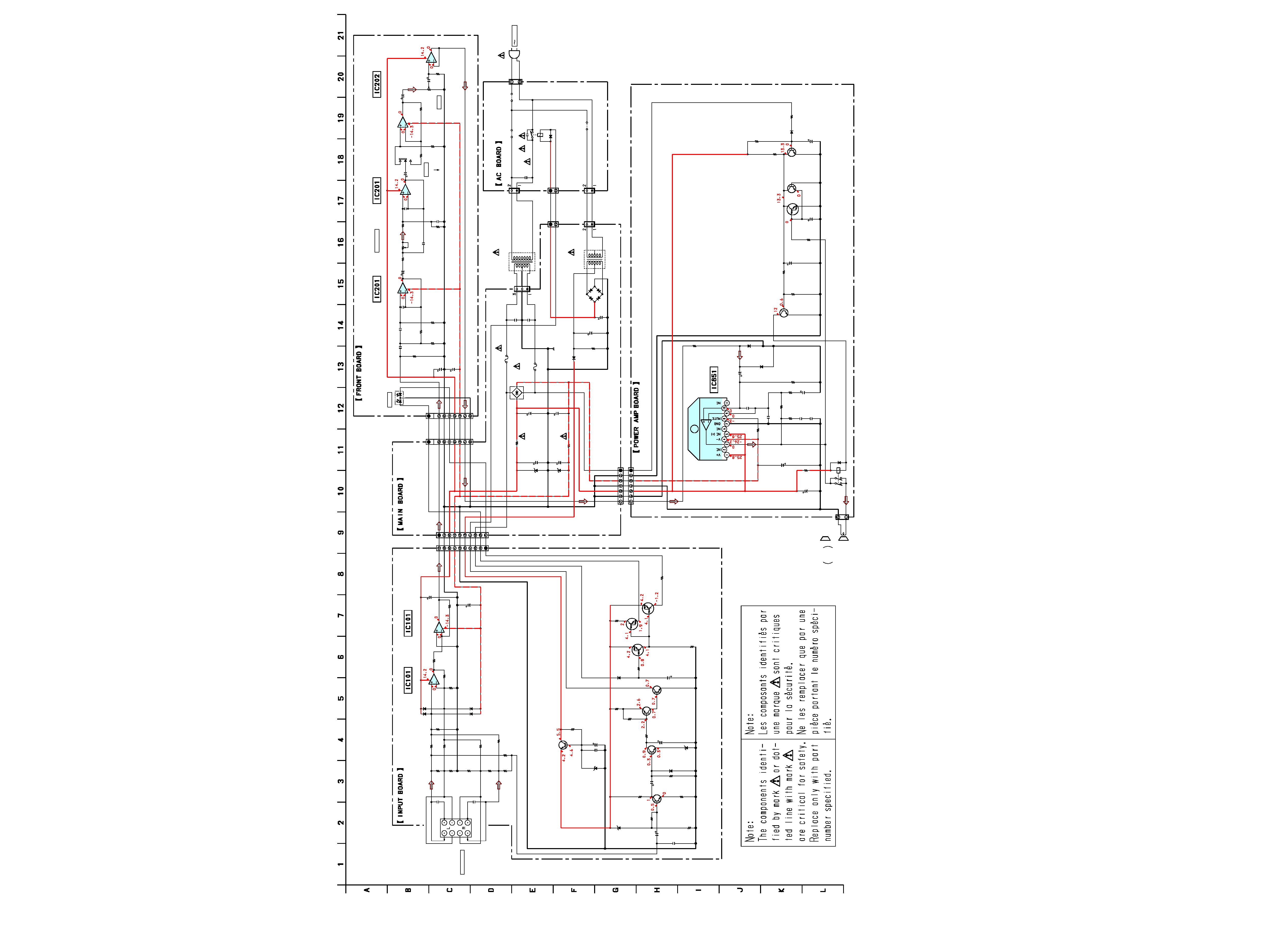
2-3. SCHEMATIC DIAGRAM
IC202(2/2)
IC202(1/2)
R208
R207
R205
R206
C204
R214
C203
R204
C212
R203
IC201(2/2)
IC201(1/2)
C103
C104
C213
R115
R117
R114
R116
D201
CN201
CN201M
IC101(2/2)
IC101(1/2)
R107
R118
R112
D104
D103
D102
D101
R103
R105
R101
R120
R122
R123
R121
R106
R102
TM101
R513
R511
R512
R510
D504
Q505
Q504
R507
R508
R509
Q503
D505
D503
R505
R503
R504
Q502
C507
R502
D502
R501
C502
D501
D455
R451
D454
D451
D452
D453
CN203M
CN203
D461
C3
JW1
CN503
JW2
D403
D404
R402
F402
C401
D401
F401
R314
D304
R313
R312
Q304
Q302
Q301
R310
R311
D303
R309
RY301
CN303
C308
C307
R307
R304
R302
R306
C302
C320
D302
D301
R111
T1
R301
IC851
C207
C210
C211
C205
C312
C305
C306
C504
C503
C506
C311
C704
C208
C209
C703
C405
C406
C451
C452
C303
C501
C505
C310
C309
R308
R401
T2
C403
C404
C402
CN502
CN502M
CN501M
CN501
CN301
CN301W
CN302
CN302W
RY461
C2
RV201
RV202
S201
R514
R515
R506
Q506
Q508
Q507
SP901
R303
Q303
Q501
C701
C711
SP902
JW3
NJM4580
NJM4580
100k
10k
10k
10k
0.068
100k
0.47
4.7k
100p
10k
NJM4580
NJM4580
0.047
0.047
100p
8.2k
1M
220k
470k
SML72423C-TP4
8P
BOARD
IN
8P
PH-L
NJM4580
NJM4580
22k
1.5k
180
1SS133
1SS133
1SS133
1SS133
180
10k
10k
4.7k
1/2W
220
1/2W
220
1/2W
4.7k
1/2W
10k
10k
SPEAKER
510
10k
220
100k
11ES2
2SC2785
2SA1175
820k
820k
10k
2SC2785
JW
1SS133
10k
1M
JW
2SC2785
0.1
100k
MTZJ-3.0A
2.2k
22000p
MTZJ-5.6A
1SS133T
4.7k
11ES2
11ES2
11ES2
11ES2
2P
PH
2P
BOARD
IN
1SS133T
0.1
275V
JW
2P
UP-S
YEW
JW
MTZJ15B
MTZJ15B
1k
2W
3.15A
125V
0.1
D3SBA20
3.15A
125V
10k
1SS133T
47k
100k
2SC2785
2SC2785
DTC124ES
100k
10k
1SS133T
22k
SPK RELAY
24V
2P
VH-L
WHT
1
1
2.2
1W
56k
22k
33k
220p
220p
1SS133T
1SS133T
10k
4.7k
LM3876-TF
4.7
50V
22
50V
22
50V
4.7
50V
10
50V
47
50V
47
50V
10
50V
4.7
50V
4.7
50V
4.7
50V
47
25V
47
25V
47
25V
47
25V
100
25V
100
25V
470
25V
470
25V
100
25V
47
25V
47
25V
100
25V
220
10V
JW
1k
2W
3300
35V
AS
3300
35V
AS
0.1
2P
2P
2P
3P
10P
10P
7P
7P
4700p
125V
20k
20k
10k
10k
10k
UN4111
10K/10K
UN4111
10K/10K
DTC114ES
10K/10K
1.5k
2SC2785
2SC2785
JW
JW
JW
IN
POWER AMP
SPK/LINE MIX
L/R MIX
HPF
+15V
-15V
GND
IN
GND
OUT
OUT
LEVEL
NUTRAL
LIVE
CP901
6
M
A
9M
A
ON/STBY
SUB TRANS
GRN-LED
RED-LED
C
H
A
S
S
IS
REVERSE
NORMAL
LEVEL
CUT OFF FREQ
CUT OFF FREQ
PHASE
INPUT/OUTPUT
POWER
TRANSFORMER
AC IN
5
6
8
7
3
2
4
1
1
4
3
2
7
6
5
8
1
2
3
4
5
6
8
7
RELAY
DRIVER
DETECT
DETECT
AC IN
Q301,302
DC LEVEL
LCD DRIVER
LCD DRIVER
INV.
RELAY
DRIVER
Q504,505
Q502,503
AUDIO
LEVEL DETECT
REG
WOOFER
PASSIVE