SERVICE MANUAL
Sony Corporation
Audio Group
Published by Sony Engineering Corporation
US Model
Canadian Model
AEP Model
UK Model
E Model
Australian Model
SURROUND SPEAKER SYSTEM
9-879-098-02
2004H16-1
© 2004.08
Ver 1.1 2004.08
SPECIFICATIONS
SA-TS22W
Surround (L)
Speaker system
Two-way Bass reflex
Speaker unit
70 mm dia. cone type,
25 mm dia. balance-dome-
type tweeter
Rated impedance
4 ohms
Dimensions (approx.)
255
× 1112 × 255 mm
(w/h/d)
Mass (approx.)
5.0 kg
General
Surround speaker (L)
Power requirements
220-240 V AC, 50/60 Hz
P
120 V AC, 60 Hz
ower consumption
36 W (220-240 V AC)
Design and specifications are subject to change
without notice.
· SA-TS22W is speaker system in
DAV-FR10W/SR4W.
2
SA-TS22W
TABLE OF CONTENTS
1.
GENERAL ................................................................... 3
2.
DIAGRAMS
2-1.
Printed Wiring Board DIAT AMP Board (Side A) ...
5
2-2.
Printed Wiring Board DIAT AMP Board (Side B) ...
6
2-3.
Schematic Diagram DIAT AMP Board (1/3) ...........
7
2-4.
Schematic Diagram DIAT AMP Board (2/3) ...........
8
2-5.
Schematic Diagram DIAT AMP Board (3/3) ...........
9
2-6.
Printed Wiring Board DIAT POWER Board ............ 10
2-7.
Schematic Diagram DIAT POWER Board ............... 11
2-8.
Printed Wiring Board DIAT BUILT PD Section ...... 12
2-9.
Schematic Diagram DIAT BUILT PD Section ......... 13
3.
EXPLODED VIEWS
3-1.
Base Cover Section .......................................................... 18
3-2.
Cabinet, Front Panel Section ........................................... 19
4.
ELECTRICAL PARTS LIST .................................. 20
SAFETY CHECK-OUT
After correcting the original service problem, perform the following
safety check before releasing the set to the customer:
Check the antenna terminals, metal trim, "metallized" knobs, screws,
and all other exposed metal parts for AC leakage.
Check leakage as described below.
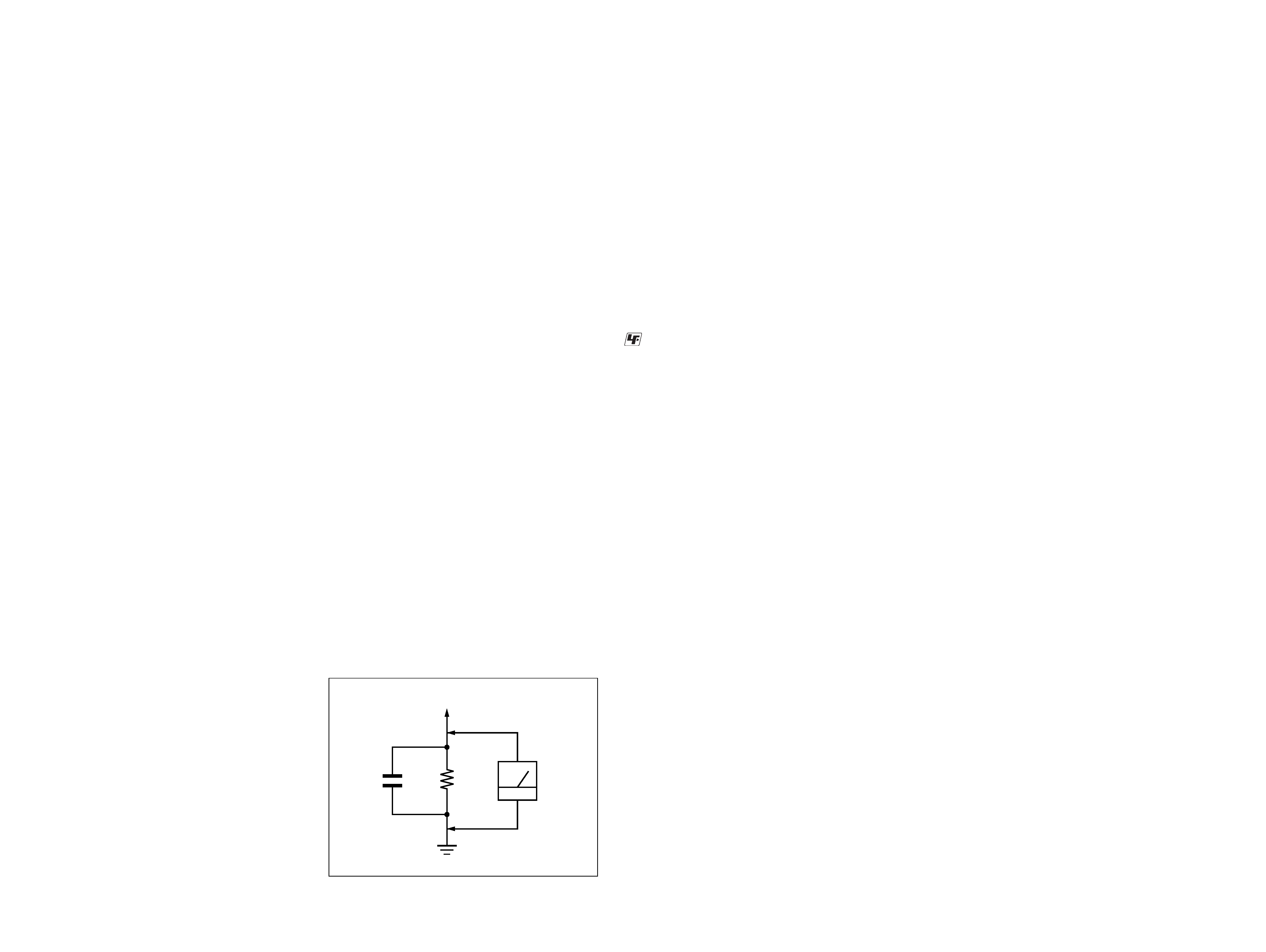
LEAKAGE TEST
The AC leakage from any exposed metal part to earth ground and
from all exposed metal parts to any exposed metal part having a
return to chassis, must not exceed 0.5 mA (500 microamperes.).
Leakage current can be measured by any one of three methods.
1. A commercial leakage tester, such as the Simpson 229 or RCA
WT-540A. Follow the manufacturers' instructions to use these
instruments.
2. A battery-operated AC milliammeter. The Data Precision 245
digital multimeter is suitable for this job.
3. Measuring the voltage drop across a resistor by means of a
VOM or battery-operated AC voltmeter. The "limit" indication
is 0.75 V, so analog meters must have an accurate low-voltage
scale. The Simpson 250 and Sanwa SH-63Trd are examples
of a passive VOM that is suitable. Nearly all battery operated
digital multimeters that have a 2 V AC range are suitable. (See
Fig. A)
Notes on chip component replacement
· Never reuse a disconnected chip component.
· Notice that the minus side of a tantalum capacitor may be
damaged by heat.
Flexible Circuit Board Repairing
· Keep the temperature of the soldering iron around 270 °C
during repairing.
· Do not touch the soldering iron on the same conductor of the
circuit board (within 3 times).
· Be careful not to apply force on the conductor when soldering
or unsoldering.
UNLEADED SOLDER
Boards requiring use of unleaded solder are printed with the lead-
free mark (LF) indicating the solder contains no lead.
(Caution: Some printed circuit boards may not come printed with
the lead free mark due to their particular size)
: LEAD FREE MARK
Unleaded solder has the following characteristics.
· Unleaded solder melts at a temperature about 40 °C higher
than ordinary solder.
Ordinary soldering irons can be used but the iron tip has to be
applied to the solder joint for a slightly longer time.
Soldering irons using a temperature regulator should be set to
about 350
°C.
Caution: The printed pattern (copper foil) may peel away if
the heated tip is applied for too long, so be careful!
· Strong viscosity
Unleaded solder is more viscou-s (sticky, less prone to flow)
than ordinary solder so use caution not to let solder bridges
occur such as on IC pins, etc.
· Usable with ordinary solder
It is best to use only unleaded solder but unleaded solder may
also be added to ordinary solder.
SAFETY-RELATED COMPONENT WARNING!!
COMPONENTS IDENTIFIED BY MARK 0 OR DOTTED LINE
WITH MARK 0 ON THE SCHEMATIC DIAGRAMS AND IN
THE PARTS LIST ARE CRITICAL TO SAFE OPERATION.
REPLACE THESE COMPONENTS WITH SONY PARTS WHOSE
PART NUMBERS APPEAR AS SHOWN IN THIS MANUAL OR
IN SUPPLEMENTS PUBLISHED BY SONY.
ATTENTION AU COMPOSANT AYANT RAPPORT
À LA SÉCURITÉ!
LES COMPOSANTS IDENTIFIÉS PAR UNE MARQUE 0 SUR
LES DIAGRAMMES SCHÉMATIQUES ET LA LISTE DES
PIÈCES
SONT
CRITIQUES
POUR
LA
SÉCURITÉ
DE
FONCTIONNEMENT. NE REMPLACER CES COM- POSANTS
QUE PAR DES PIÈCES SONY DONT LES NUMÉROS SONT
DONNÉS DANS CE MANUEL OU DANS LES SUPPLÉMENTS
PUBLIÉS PAR SONY.
1.5 k
0.15
µF
AC
voltmeter
(0.75 V)
To Exposed Metal
Parts on Set
Earth Ground
Fig. A.
Using an AC voltmeter to check AC leakage.
3
SA-TS22W
SECTION 1
GENERAL
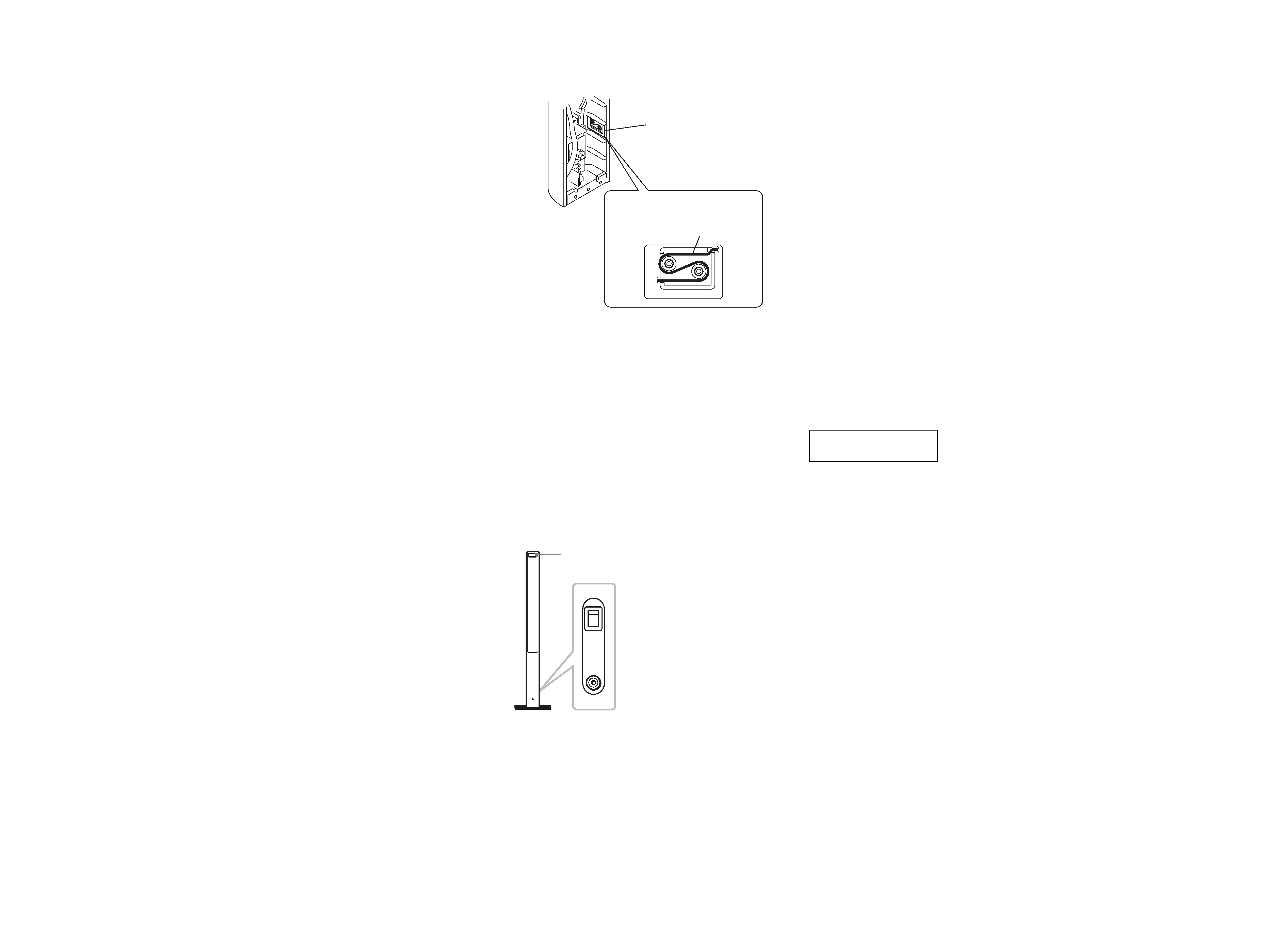
Surround speaker (L)
The surround speaker (L) incorporates the IR receiver. It receives the sound from the IR transmitter and
sends it to the surround speaker (R).
Connect the surround speaker (R).
ON
OFF
ONLY FOR
POWER
DIR-R2
Rear side of the surround speaker (L)
IR receiver
This section is extracted
from instruction manual.
SERVICING NOTE
4-246-444-01
After service, as shown in a figure,
a power cord is fixed.
power cord
Label
Ver 1.1
4
SA-TS22W
SECTION 2
DIAGRAMS
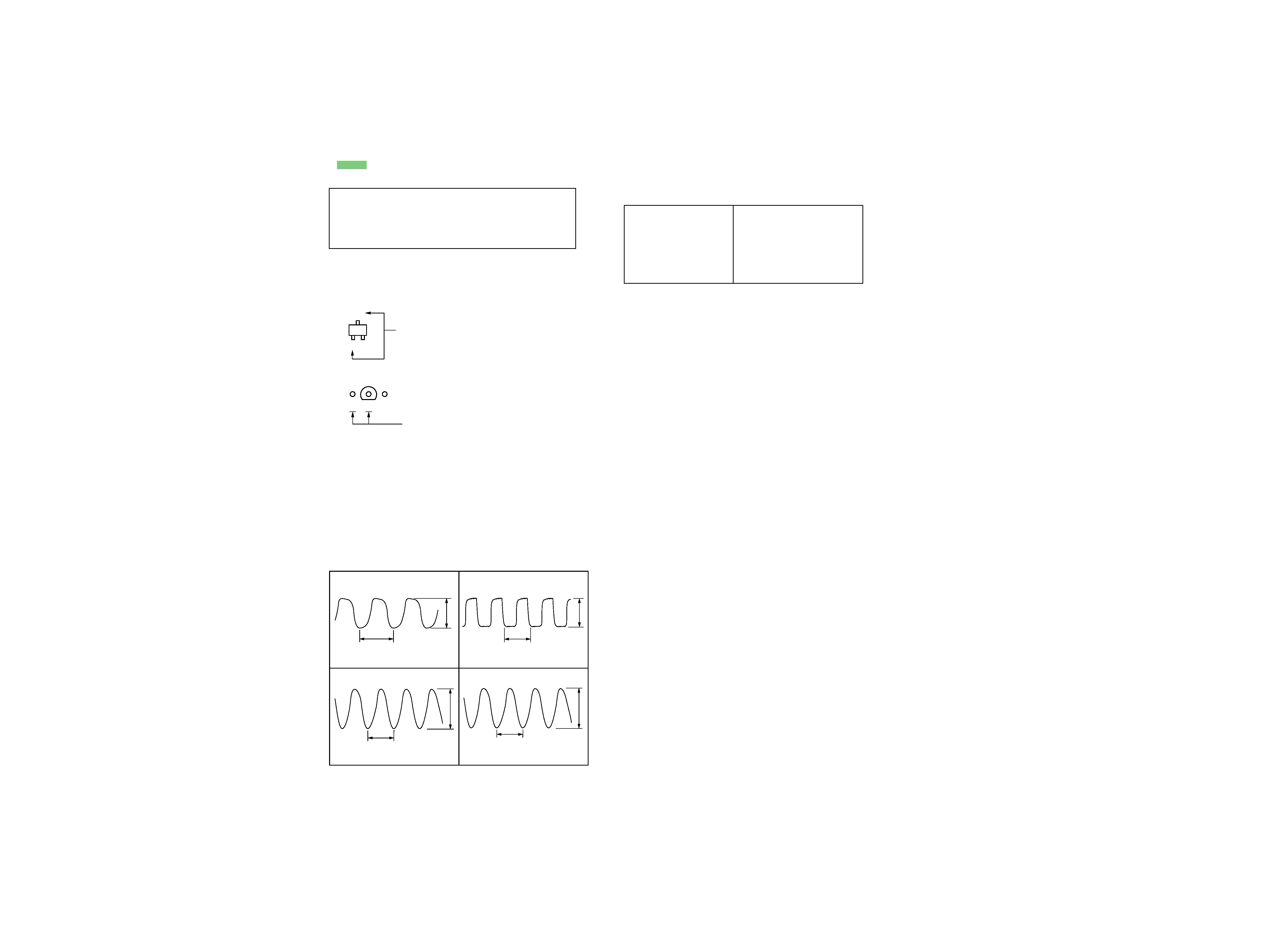
·Waveforms
DIAT AMP Board
4 IC114 4
2 IC102 tf (BCK)
1 IC102 rd (OSCO)
3 IC107 wd (X1)
20.3 ns
4.5 Vp-p
125 ns
3.5 Vp-p
325 ns
2.5 Vp-p
81.3 ns
1 V/DIV, 50 ns/DIV
1 V/DIV, 50 ns/DIV
2 V/DIV, 10 ns/DIV
1 V/DIV, 100 ns/DIV
2.5 Vp-p
Note on Schematic Diagrams:
· All capacitors are in
µF unless otherwise noted. (p: pF)
50 WV or less are not indicated except for electrolytics and
tantalums.
· All resistors are in
and 1/4 W or less unless otherwise
specified.
· C : panel designation.
· A : B+ Line.
·Voltages and waveforms are dc with respect to ground
under no-signal (detuned) conditions.
: Impossible to measure
·Voltages are taken with a VOM (Input impedance 10 M
).
Voltage variations may be noted due to normal production
tolerances.
·Waveforms are taken with a oscilloscope.
Voltage variations may be noted due to normal production
tolerances.
· Circled numbers refer to waveforms.
· Signal path.
F
: AUDIO
·Abbreviation
CND
: Canadian model
MX
: Mexican model
TW
: Taiwan model
Note on Printed Wiring Boards:
· X : parts extracted from the component side.
· Y : parts extracted from the conductor side.
·
: Pattern from the side which enables seeing.
(The other layers' patterns are not indicated.)
· DIAT AMP board is multi-layer printed board.
However, the patterns of intermediate layers have not been
included in diagrams.
· Indication of transistor.
· Note for Printed Wiring Boards and Schematic Diagrams
C
B
These are omitted.
E
Q
Caution:
Pattern face side:
Parts on the pattern face side seen from
(Conductor Side)
the pattern face are indicated.
Parts face side:
Parts on the parts face side seen from
(Component Side) the parts face are indicated.
B
These are omitted.
CE
Q
Note:
The components identi-
fied by mark 0 or dot-
ted line with mark 0 are
critical for safety.
Replace only with part
number specified.
Note:
Les composants identifiés
par une marque 0 sont cri-
tiques pour la sécurité.
Ne les remplacer que par une
piéce por tant le numéro
spécifié.
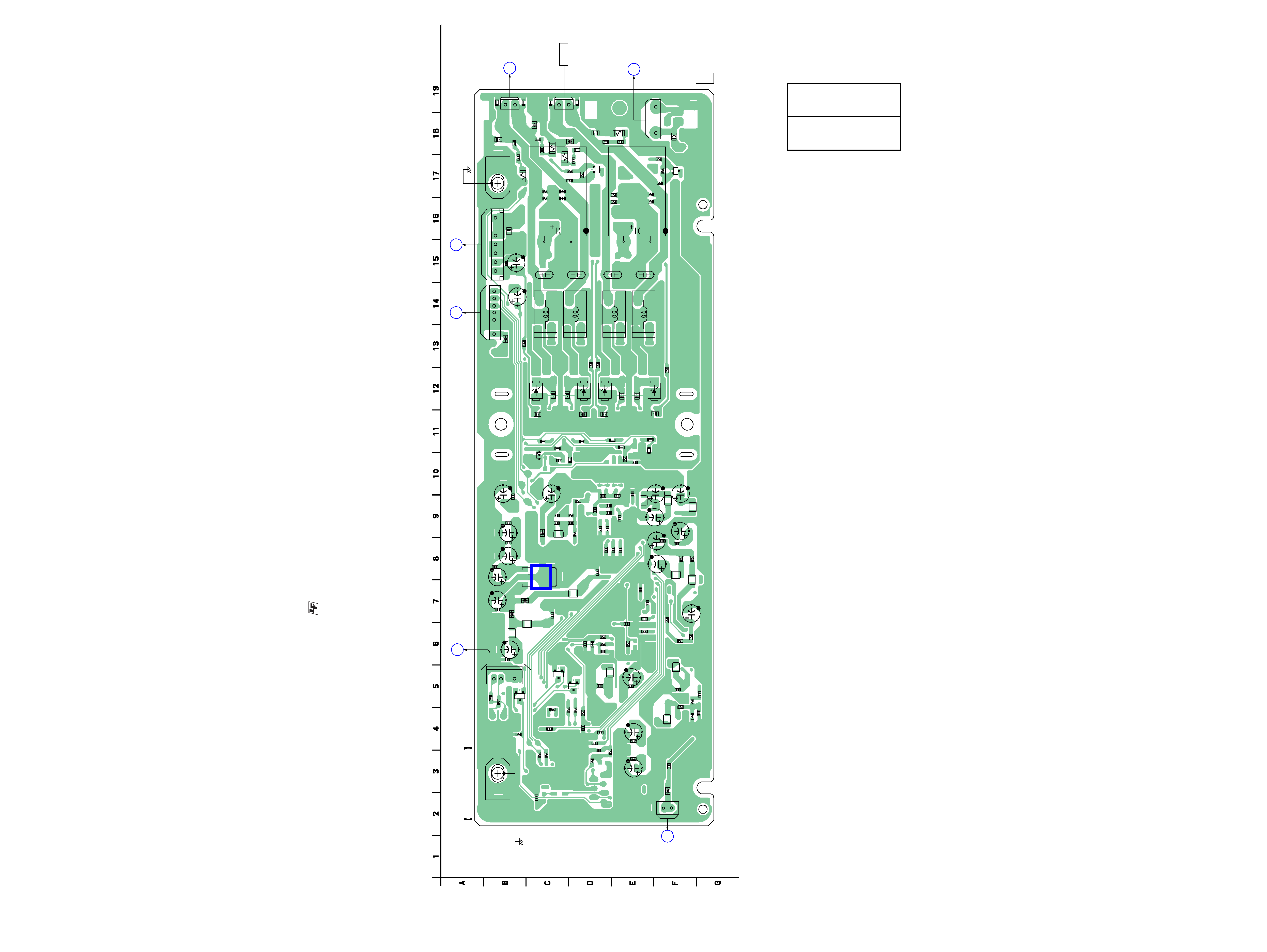
5
5
SA-TS22W
SA-TS22W
2-1. PRINTED WIRING BOARD -- DIAT AMP BOARD (SIDE A) --
:Uses unleaded solder.
CNP102
CNP106
CNP103
C199
C229
C235
EB101
EB102
C214
CN302
C161
C128
C163
L112
C137
C136
C104
C107
C102
L115
C168
L118
C228
L121
C225
C150
C140
C230
C179
C202
C178
Q110
Q106
R171
R222
FB109
C259
C152
C167
R100
R125
R196
C257
R220
C226
C195
R210
R143
C151
L106
C133
L109
L107
C130
C119
R108
C114
R165
R136
R126
C115
R105
C157
R103
D115
R178
C162
C160
C185
FB106
C177
FB107
C155
R164
C154
C135
C138
C197
C103
C101
C256
C153
C182
C213
R106
R186
C183
C200
C203
C231
C193
R169
C236
R177
C170
R185
C189
R142
C209
R211
C210
C238
R139
C217
R191
R159
R154
R195
C201
R156
C194
R203
C218
C232
C171
Q109
R153
R254
R157
L104
FB104
FB105
IC108
C109
R158
C258
CN105
CN104
L105
C175
L108
C224
R209
R206
R204
C223
C227
C127
C141
C134
R205
R207
R208
L111
FB108
L110
C187
R200
C219
R201
C237
L122
C220
C172
C176
C173
R194
L116
C205
C206
C196
C198
R188
R197
C215
C188
R179
R166
D105
D106
D107
D104
R138
Q104
Q103
FB103
R312
R313
R314
R263
C204
C149
C212
C216
C192
C184
R256
FB301
C306
CN301
C310
C301
C309
R301
R303
R302
L302
L303
E
E
E
E
E
(SIDE A)
DIAT AMP BOARD
1-862-468-
12
(12)
(CHASSIS)
SPEAKER
(CHASSIS)
1
6
6
1
DIAT POWER
BOARD
CN904
(Page 10)
C
DIAT POWER
BOARD
CN905
(Page 10)
B
1
3
POWER LED
BOARD
CNP400
(Page 12)
A
1
3
2
DIAT BUILT
PD BOARD
CN7301
(Page 12)
E
PIN JACK
BOARD
CN303
(Page 12)
F
SPEAKER
JACK
BOARD
CN100
(Page 12)
D
· Semiconductor
Location
Ref. No.
Location
D104
E-12
D105
D-12
D106
D-12
D107
C-12
D115
C-10
IC108
C-8
Q103
D-5
Q104
C-5
Q106
D-17
Q109
F-17
Q110
B-5