SERVICE MANUAL
US Model
Canadian Model
AEP Model
UK Model
Australian Model
Chinese Model
Hong Kong Model
SACD/DVD PLAYER
DVP-S9000ES
RMT-D122A/D122E/D122O/D122P
SPECIFICATIONS
Photo: Gold type
SACD/DVD player
Laser
Semiconductor laser
Signal format system
PAL/(NTSC)
Audio characteristics
Frequency response
DVD (PCM 96 kHz): 2 Hz to 44 kHz
(2 dB
±1 dB at 44 kHz)
CD: 2 Hz to 20 kHz (
±0.5 dB)
SACD: 2 Hz to 100 kHz (3 dB
±1 dB at 50
kHz)
Signal to noise ratio
more than 115 dB (DVD)
Harmonic distortion
DVD: Less than 0.0015%
CD: Less than 0.002%
SACD: Less than 0.0015%
Dynamic range
More than 103 dB (DVD)
More than 103 dB (SACD)
More than 99 dB (CD)
Wow and flutter
Less than detected value
(
±0.001% W PEAK)
Outputs
AUDIO OUT
(1, 2)
DIGITAL OUT
(OPTICAL)
DIGITAL OUT
(COAXIAL)
VIDEO OUT
S VIDEO OUT
COMPONENT
VIDEO OUT
(Y, PB/CB,
PR/CR)
General
Power requirements
220
120 V AC, 60Hz (EXCETP US, Canadian)
- 240 V AC, 50/60 Hz
Power consumption
48
43 W (EXCEPT US, Canadian)
W
Dimensions (approx.)
430
126
398 mm (17
× 5 ×
××
15 11/16 in.)
(w/h/d) incl. projecting parts
Mass (approx.)
12.6 kg (27 lb 12 oz)
Operating temperature
5 °C to 35 °C (41 °F to 95 °F)
Operating humidity
25%to80%
Supplied accessories
Design and specifications are subject to change without notice.
Jack
type
Phono
jacks
Optical
output
connector
Phono
jack
Phono
jacks
4-pin
mini DIN
Phono
jacks
Output
level
2 Vrms
(at 50 kilohms)
18 dBm
0.5 Vp-p
1.0 Vp-p
Y: 1.0 Vp-p
C: 0.3 Vp-p
(PAL)
(EXCEPT US,
Canadian)
C: 0.286 Vp-p
(NTSC)
Y: 1.0 Vp-p
PB/CB,
PR/CR:
±0.35 Vp-p
Load impedance
Over 10 kilohms
Wave length: 660 nm
75 ohms terminated
75 ohms,
sync negative
75 ohms,
sync negative
75 ohms terminated
75 ohms,
sync negative
75 ohms
Check that you have the following items:
· Audio connecting cord (1)
· Video connecting cord (1)
· S-link (Control S) connecting cord (1)
· S video cord (1)
· Power cord (1)
· Remote commander (remote) (1)
· Size AA (R6) batteries (2)
2
WARNING!!
WHEN SERVICING, DO NOT APPROACH THE LASER
EXIT WITH THE EYE TOO CLOSELY. IN CASE IT IS
NECESSARY TO CONFIRM LASER BEAM EMISSION,
BE SURE TO OBSERVE FROM A DISTANCE OF
MORE THAN 25 cm FROM THE SURFACE OF THE
OBJECTIVE LENS ON THE OPTICAL PICK-UP BLOCK.
CAUTION
Use of controls or adjustments or performance of procedures
other than those specified herein may result in hazardous ra-
diation exposure.
ATTENTION AU COMPOSANT AYANT RAPPORT
À LA SÉCURITÉ!
LES COMPOSANTS IDENTIFIÉS PAR UNE MARQUE 0
SUR LES DIAGRAMMES SCHÉMATIQUES ET LA LISTE
DES PIÈCES SONT CRITIQUES POUR LA SÉCURITÉ
DE FONCTIONNEMENT. NE REMPLACER CES COM-
POSANTS QUE PAR DES PIÈCES SONY DONT LES
NUMÉROS SONT DONNÉS DANS CE MANUEL OU
DANS LES SUPPLÉMENTS PUBLIÉS PAR SONY.
SAFETY-RELATED COMPONENT WARNING!!
COMPONENTS IDENTIFIED BY MARK 0 OR DOTTED
LINE WITH MARK 0 ON THE SCHEMATIC DIAGRAMS
AND IN THE PARTS LIST ARE CRITICAL TO SAFE
OPERATION. REPLACE THESE COMPONENTS WITH
SONY PARTS WHOSE PART NUMBERS APPEAR AS
SHOWN IN THIS MANUAL OR IN SUPPLEMENTS PUB-
LISHED BY SONY.
CAUTION:
The use of optical instrument with this product will increase eye
hazard.
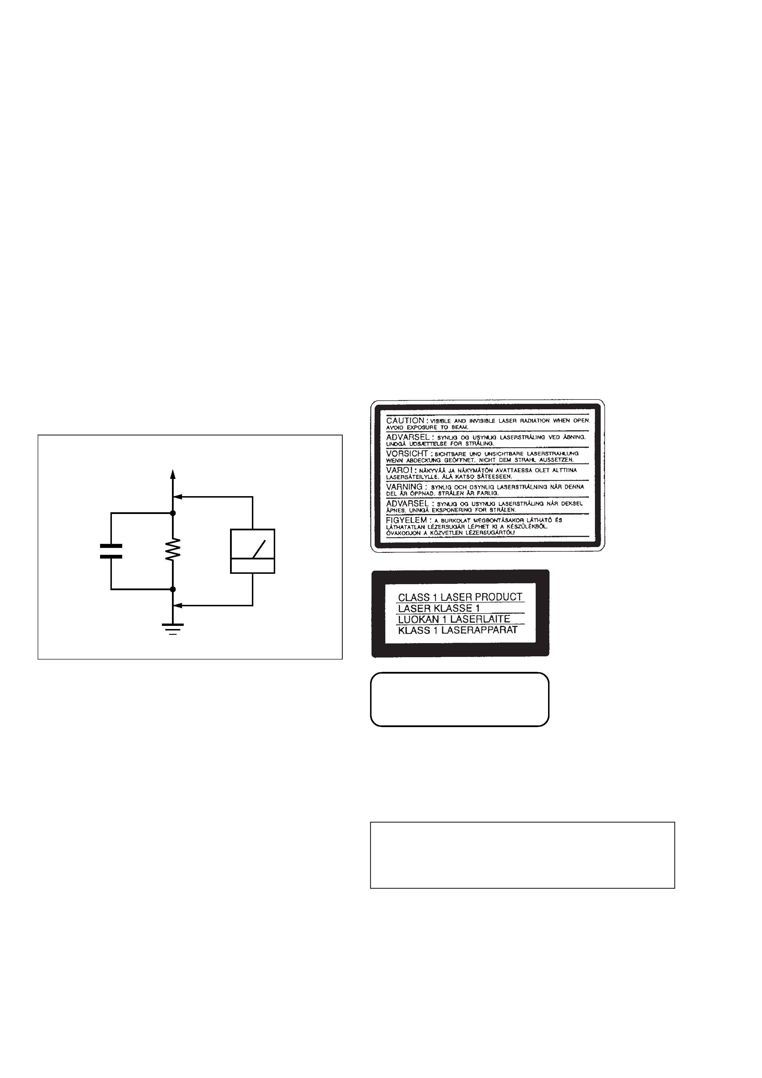
Fig. A.
Using an AC voltmeter to check AC leakage.
1.5 k
0.15
µF
AC
voltmeter
(0.75 V)
To Exposed Metal
Parts on Set
Earth Ground
LEAKAGE TEST
The AC leakage from any exposed metal part to earth ground
and from all exposed metal parts to any exposed metal part having
a return to chassis, must not exceed 0.5 mA (500 microamperes).
Leakage current can be measured by any one of three methods.
1. A commercial leakage tester, such as the Simpson 229 or RCA
WT-540A. Follow the manufacturers' instructions to use these
instruments.
2. A battery-operated AC milliammeter. The Data Precision 245
digital multimeter is suitable for this job.
3. Measuring the voltage drop across a resistor by means of a
VOM or battery-operated AC voltmeter. The "limit" indica-
tion is 0.75V, so analog meters must have an accurate low-
voltage scale. The Simpson 250 and Sanwa SH-63Trd are ex-
amples of a passive VOM that is suitable. Nearly all battery
operated digital multimeters that have a 2V AC range are suit-
able. (See Fig. A)
1. Check the area of your repair for unsoldered or poorly-sol-
dered connections. Check the entire board surface for solder
splashes and bridges.
2. Check the interboard wiring to ensure that no wires are
"pinched" or contact high-wattage resistors.
3. Look for unauthorized replacement parts, particularly transis-
tors, that were installed during a previous repair. Point them
out to the customer and recommend their replacement.
4. Look for parts which, though functioning, show obvious signs
of deterioration. Point them out to the customer and recom-
mend their replacement.
5. Check the line cord for cracks and abrasion. Recommend the
replacement of any such line cord to the customer.
6. Check the B+ voltage to see it is at the values specified.
7. Check the antenna terminals, metal trim, "metallized" knobs,
screws, and all other exposed metal parts for AC leakage.
Check leakage as described below.
SAFETY CHECK-OUT
After correcting the original service problem, perform the following
safety checks before releasing the set to the customer:
CLASS 3B LASER
LUOKAN 3B LASER
LASERKLASS 3B

3
Service Note .......................................................................... 5
1.
GENERAL
This Player Can Play the Following Discs .................. 1-1
Getting Started ............................................................ 1-2
Playing Discs ............................................................... 1-4
Using Various Functions with the Control Menu ......... 1-6
Settings and Adjustments ........................................... 1-12
Additional Information ................................................. 1-16
2.
DISASSEMBLY
2-1.
Top Case Removal ...................................................... 2-1
2-2.
Front Panel Removal ................................................... 2-1
2-3.
FL-114 Board Removal ............................................... 2-1
2-4.
MB-91 Board Removal ................................................ 2-1
2-5.
PS-436/437/438/439 Board Removal ......................... 2-2
2-6.
AV-226 Board Removal ............................................... 2-2
2-7.
Mechanism Deck Removal .......................................... 2-2
2-8.
TK-58 Board Removal ................................................. 2-2
2-9.
Loading Assembly Removal ........................................ 2-3
2-10. Optical Pick-up Removal ............................................. 2-3
2-11. Base Assembly Removal ............................................ 2-3
2-12. Internal View ................................................................ 2-4
2-13. Circuit Boards Location ............................................... 2-5
3.
BLOCK DIAGRAMS
3-1.
Overall Block Diagram ................................................. 3-1
3-2.
RF/Servo Block Diagram ............................................. 3-3
3-3.
Signal Process 1 Block Diagram ................................. 3-5
3-4.
Signal Process 2 Block Diagram ................................. 3-7
3-5.
Video 1 Block Diagram ................................................ 3-9
3-6.
Video 2 Block Diagram ................................................ 3-11
3-7.
System Control Block Diagram ................................... 3-13
3-8.
Audio Block Diagram ................................................... 3-15
3-9.
Interface Control Block Diagram ................................. 3-17
3-10. Power 1 Block Diagram ............................................... 3-19
3-11. Power 2 Block Diagram ............................................... 3-21
4.
PRINTED WIRING BOARDS AND
SCHEMATIC DIAGRAMS
4-1.
Frame Schematic Diagram .......................................... 4-3
Frame (1) Schematic Diagram .................................... 4-3
Frame (2) Schematic Diagram .................................... 4-5
4-2.
Printed Wiring Boards and Schematic Diagrams ....... 4-7
TK-58 Printed Wiring Board ........................................ 4-7
TK-58 (RW GAIN CONTROL) Schematic Diagram .... 4-11
TK-58 (RF AMP) Schematic Diagram ......................... 4-13
MB-91 Printed Wiring Board ....................................... 4-15
MB-91 (AV DECODER) Schematic Diagram .............. 4-19
MB-91 (SDRAM) Schematic Diagram ........................ 4-21
MB-91 (SERVO DSP) Schematic Diagram ................. 4-23
MB-91 (DRIVE) Schematic Diagram .......................... 4-25
MB-91 (ARP3) Schematic Diagram ............................ 4-27
MB-91 (SYSTEM CONTROL) Schematic Diagram .... 4-29
MB-91 (ROM/RAM) Schematic Diagram .................... 4-31
MB-91 (H2GA) Schematic Diagram ............................ 4-33
MB-91 (MIP) Schematic Diagram ............................... 4-35
MB-91 (OSD) Schematic Diagram .............................. 4-37
MB-91 (SDRAM) Schematic Diagram ........................ 4-39
MB-91 (PRAWN) Schematic Diagram ........................ 4-41
VP-52 Printed Wiring Board ........................................ 4-43
VP-52 (TBC) Schematic Diagram ............................... 4-47
VP-52 (VIDEO ENCODER) Schematic Diagram ........ 4-49
VP-52 (PROGRESSIVE) Schematic Diagram ............ 4-51
VP-52 (SGRAM) Schematic Diagram ......................... 4-53
VP-52 (D/A CONVERTER) Schematic Diagram ........ 4-55
VP-52 (VIDEO BUFFER) Schematic Diagram ........... 4-57
AU-226, CO-26 Printed Wiring Boards ....................... 4-59
AU-226 (D/A CONVERTER, DIGITAL FILTER),
CO-26 (DIGITAL OUT COAXIAL JACK)
Schematic Diagram ..................................................... 4-63
AU-226 (CURRENT PULSE D/A, AMP)
Schematic Diagram ..................................................... 4-65
ER-11 Printed Wiring Board ........................................ 4-67
ER-11 (EURO AV1) Schematic Diagram .................... 4-71
ER-11 (EURO AV2) Schematic Diagram .................... 4-73
FL-114 Printed Wiring Board ...................................... 4-75
BZ-1 Printed Wiring Board .......................................... 4-78
FL-114 (IF CON) Schematic Diagram ........................ 4-79
FL-114 (LED DRIVE), BZ-1 (BUZZER)
Schematic Diagram ..................................................... 4-81
FR-172 Printed Wiring Board ...................................... 4-83
FR-172 (DC-DC CONVERTER, REMOTE
COMMANDER RECEIVER) Schematic Diagram ....... 4-85
AC-113/114, SW-344 Printed Wiring Boards .............. 4-87
AC-113/114 (STANDBY),
SW-344 (POWER SWITCH) Schematic Diagram ...... 4-91
MS-59 (LOADING MOTOR), CK-95 (SENSOR)
Printed Wiring Boards and Schematic Diagram ......... 4-93
PS-436/438 Printed Wiring Board ............................... 4-95
PS-436/438 (POWER SUPPLY)
Schematic Diagram ..................................................... 4-99
PS-437/439 (POWER SUPPLY)
Schematic Diagram ..................................................... 4-101
PS-437/439 Printed Wiring Board ............................... 4-103
5.
IC PIN FUNCTION DESCRIPTION
5-1.
System Control Pin Function
(MB-91 Board IC102) .................................................. 5-1
6.
TEST MODE
6-1.
General Description ...................................................... 6-1
6-2.
Starting Test Mode ........................................................ 6-1
6-3.
Syscon Diagnosis .......................................................... 6-1
6-4.
Drive Auto Adjustment .................................................. 6-5
6-5.
Drive Manual Operation ................................................ 6-7
6-6.
Mecha Aging ................................................................. 6-9
6-7.
Emergency History ........................................................ 6-9
6-8.
Version Information ....................................................... 6-10
6-9.
Video Level Adjustment ................................................ 6-10
6-10. If Con Self Diagnostic Function .................................... 6-11
7.
ELECTRICAL ADJUSTMENTS
7-1.
Power Supply Check ................................................... 7-1
1.
AC-113 Board .............................................................. 7-1
2.
PS-436 Board .............................................................. 7-1
3.
PS-437 Board .............................................................. 7-1
7-2.
Adjustment of System Control .................................... 7-2
1.
System Clock 27 MHz Adjustment ............................. 7-2
7-3.
Adjustment of Video System ....................................... 7-2
1.
Interface Video Output Level Adjustment ................... 7-2
2.
S-terminal Output Check ............................................. 7-2
3.
Checking Component Video Output B-Y .................... 7-2
4.
Checking Component Video Output R-Y .................... 7-3
5.
Component Video Output Level Adjustment ............... 7-3
6.
Progressive Video Output Level Adjustment .............. 7-3
7.
Checking RGB Output R ............................................. 7-3
8.
Checking RGB Output G ............................................. 7-4
TABLE OF CONTENTS
Section
Title
Page
Section
Title
Page

4
9.
Checking RGB Output B (AEP, UK Model) ................. 7-4
10.
Checking S Video Output S-C ..................................... 7-4
7-4.
Adjustment Related Parts Arrangement ..................... 7-6
8.
REPAIR PARTS LIST
8-1.
Exploded Views ........................................................... 8-1
8-1-1. Case Assembly ...................................................... 8-1
8-1-2. Chassis Assembly .................................................. 8-2
8-1-3. Mechanism Deck Assembly ................................... 8-3
8-2.
Electrical Parts List ..................................................... 8-4
Section
Title
Page
5
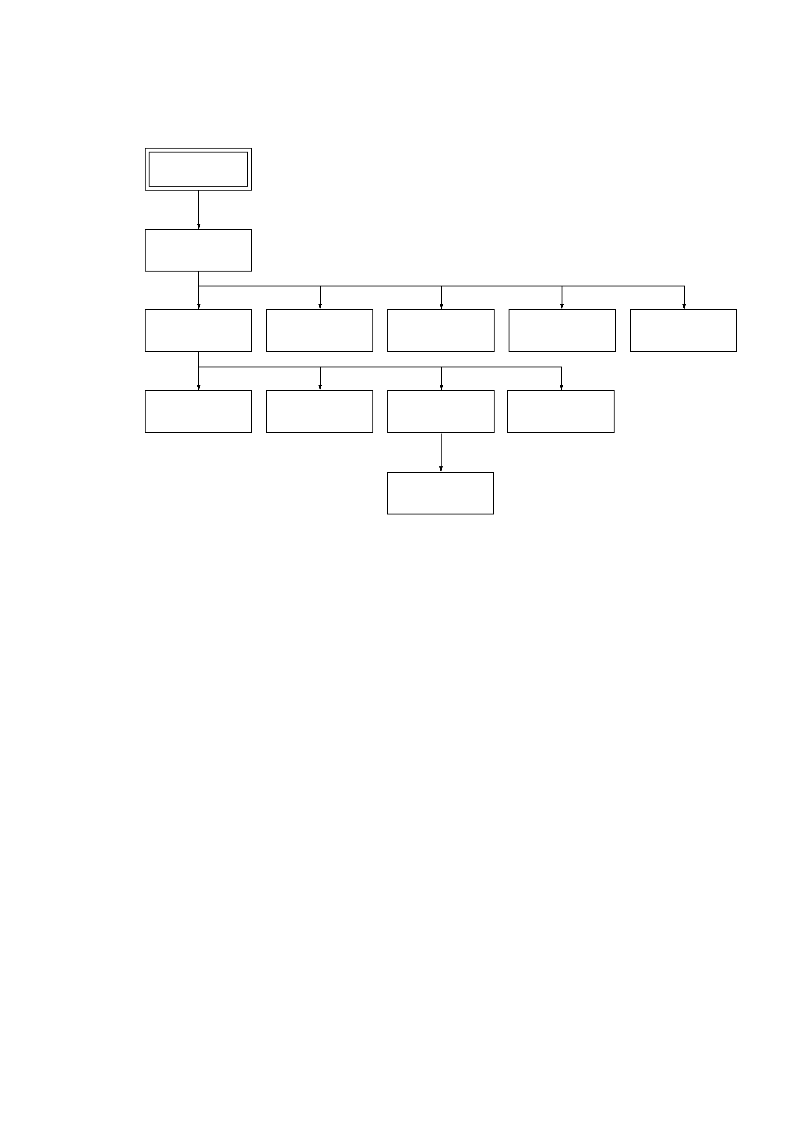
SERVICE NOTE
1.
DISASSEMBLY
· This set can be disassembled in the order shown below.
Set
Top Case
(Page 2-1)
Front Panel
(Page 2-1)
Mechanism Deck
(Page 2-2)
MB-91 Board
(Page 2-1)
AU-226 Board
(Page 2-2)
PS-436/437/438/439
Board
(Page 2-2)
FL-114 Board
(Page 2-1)
Optical Pick-up
(Page 2-3)
TK-58 Board
(Page 2-2)
Loading Assembly
(Page 2-3)
Base Assembly
(Page 2-3)