SERVICE MANUAL
Sony Corporation
Home Audio Company
Published by Sony Engineering Corporation
US Model
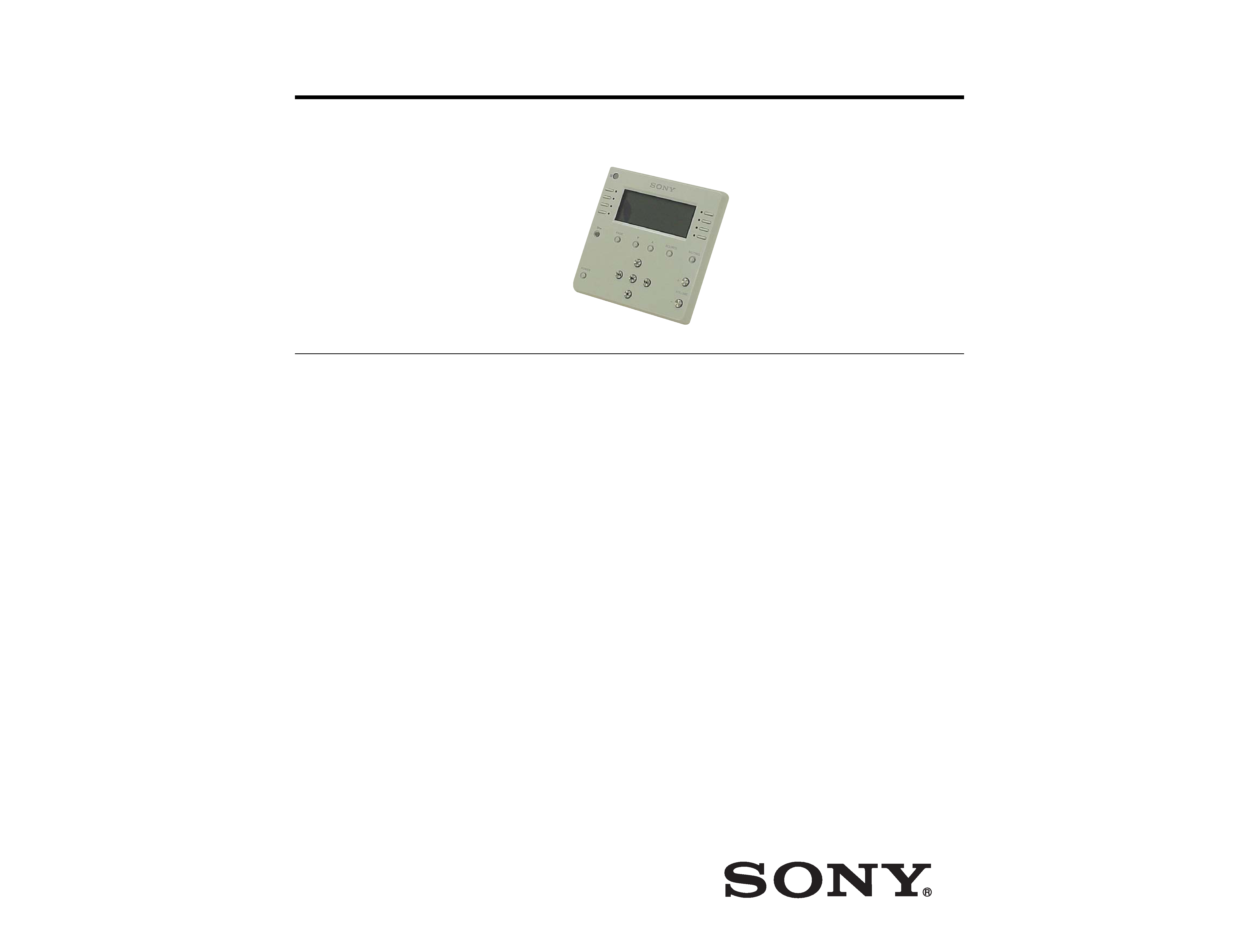
KEYPAD
9-877-895-01
2004E16-1
© 2004.05
Ver 1.0 2004.05
SPECIFICATIONS
RMR-K100
Operating system:Wired controller
LCD size:3 inches (80
36 dots)
LCD type:Reflection system (mirror type)
Power requirements:
Connect to CAV-M1000ES via CAT5 cable
Maximum external dimensions:
125
125 53mm (5 5 2 1/8 inches)
(w/h/d, including projecting part and controls)
Mass:
240 g (8 oz)
Supplied accessories:
Bracket frame for KEYPAD attachment to a junction box
Screw B2
8 for fixing KEYPAD to a Keypad mounting bracket (2)
Screw M3
30 for Keypad mounting bracket fixing to a junction box (4)
RM-KP10 IR Remote Control for the Keypad
Design and specifications are subject to change without notice.

2
RMR-K100
Notes on chip component replacement
·Never reuse a disconnected chip component.
·
Notice that the minus side of a tantalum capacitor may be
damaged by heat.
Flexible Circuit Board Repairing
·Keep the temperature of soldering iron around 270°C during
repairing.
·
Do not touch the soldering iron on the same conductor of the
circuit board (within 3 times).
·
Be careful not to apply force on the conductor when soldering
or unsoldering.
TABLE OF CONTENTS
SAFETY-RELATED COMPONENT WARNING!!
COMPONENTS IDENTIFIED BY MARK 0 OR DOTTED LINE WITH
MARK 0 ON THE SCHEMATIC DIAGRAMS AND IN THE PARTS
LIST ARE CRITICAL TO SAFE OPERATION. REPLACE THESE
COMPONENTS WITH SONY PARTS WHOSE PART NUMBERS
APPEAR AS SHOWN IN THIS MANUAL OR IN SUPPLEMENTS
PUBLISHED BY SONY.
1.
GENERAL ................................................................... 3
2.
DIAGRAMS
2-1.
Block Diagram ................................................................
6
2-2.
Printed Wiring Board
Front Display Board (Side A) ....................................
7
2-3.
Printed Wiring Board
Front Display Board (Side B) ...................................
8
2-4.
Schematic Diagram Front Display Board .................
9
2-5.
Printed Wiring Board Bottom Supply Board ............ 10
2-6.
Schematic Diagram Bottom Supply Board ............... 11
3.
EXPLODED VIEWS ................................................. 13
4.
ELECTRICAL PARTS LIST .................................. 14
UNLEADED SOLDER
Boards requiring use of unleaded solder are printed with the lead-
free mark (LF) indicating the solder contains no lead.
(Caution: Some printed circuit boards may not come printed with
the lead free mark due to their particular size)
: LEAD FREE MARK
Unleaded solder has the following characteristics.
· Unleaded solder melts at a temperature about 40 °C higher
than ordinary solder.
Ordinary soldering irons can be used but the iron tip has to be
applied to the solder joint for a slightly longer time.
Soldering irons using a temperature regulator should be set to
about 350
°C.
Caution: The printed pattern (copper foil) may peel away if
the heated tip is applied for too long, so be careful!
· Strong viscosity
Unleaded solder is more viscou-s (sticky, less prone to flow)
than ordinary solder so use caution not to let solder bridges
occur such as on IC pins, etc.
· Usable with ordinary solder
It is best to use only unleaded solder but unleaded solder may
also be added to ordinary solder.
3
RMR-K100
SECTION 1
GENERAL
This section is extracted
from instruction manual.
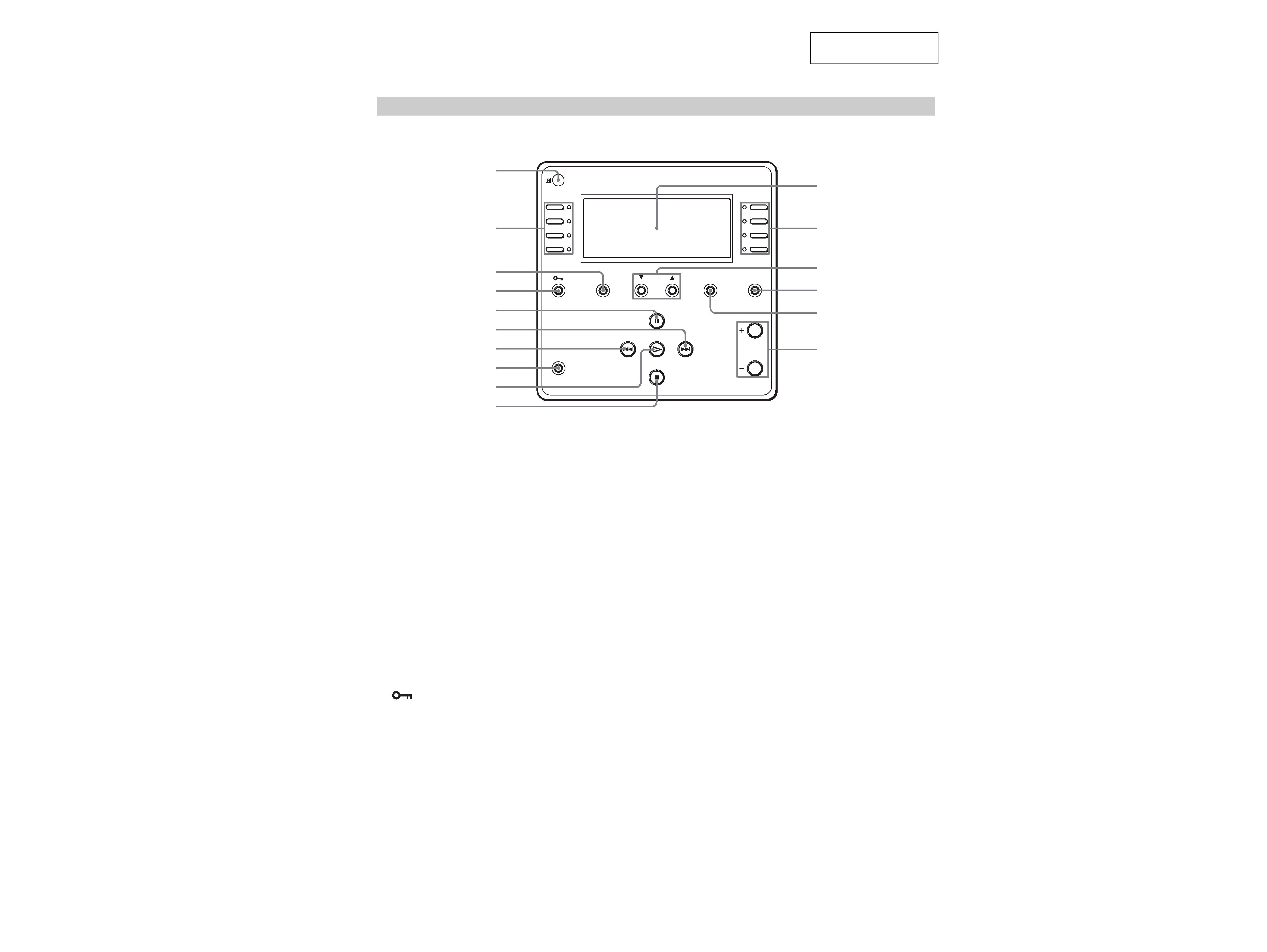
Front panel of the Keypad
1
IR sensor
Receives IR signals from the IR Remote Control for the
Keypad (supplied) to control both source components
and the system.
2
SELECT
Press to select a menu on the LCD display, such as a
source menu, a disc title list, etc.
The LED next to the SELECT button lights as follows
on the source selection:
green: selected in the own zone
amber: selected and locked in the other zone.
3
PAGE
Press to return to the previous menu or to view the
current status of the disc title list and the preset station
list. If there is no list, only a source name will be
displayed.
4
(LOCK)
Press to lock the selected source.
amber: locked
off: released
5
X
(PAUSE)
Press to pause the playback.
PAGE
SOURCE
MUTING
VOLUME
POWER
qa
2
qs
qf
qd
qg
1
2
3
4
5
6
7
8
9
0
6
>
Press to advance the track/title or to select a preset
station.
7
.
Press to go reverse the track/title or to select a preset
station.
8
POWER switch
Press to turn the power of the Keypad on or off.
9
N
(PLAY)
Press to operate the selected source.
0
x
(STOP)
Press to stop playback.
qa
Display window
Displays the selected source, the zone volume level,
the zone and the system status, and other system
status information.
qs
v
/V (SCROLL UP/DOWN)
Press to scroll the LCD menu.
qd
MUTING
Press to mute the speaker output in the zone.
qf
SOURCE
Press to return to the source components list screen.
qg
VOLUME +/
Press to adjust the volume in a zone.
4
RMR-K100
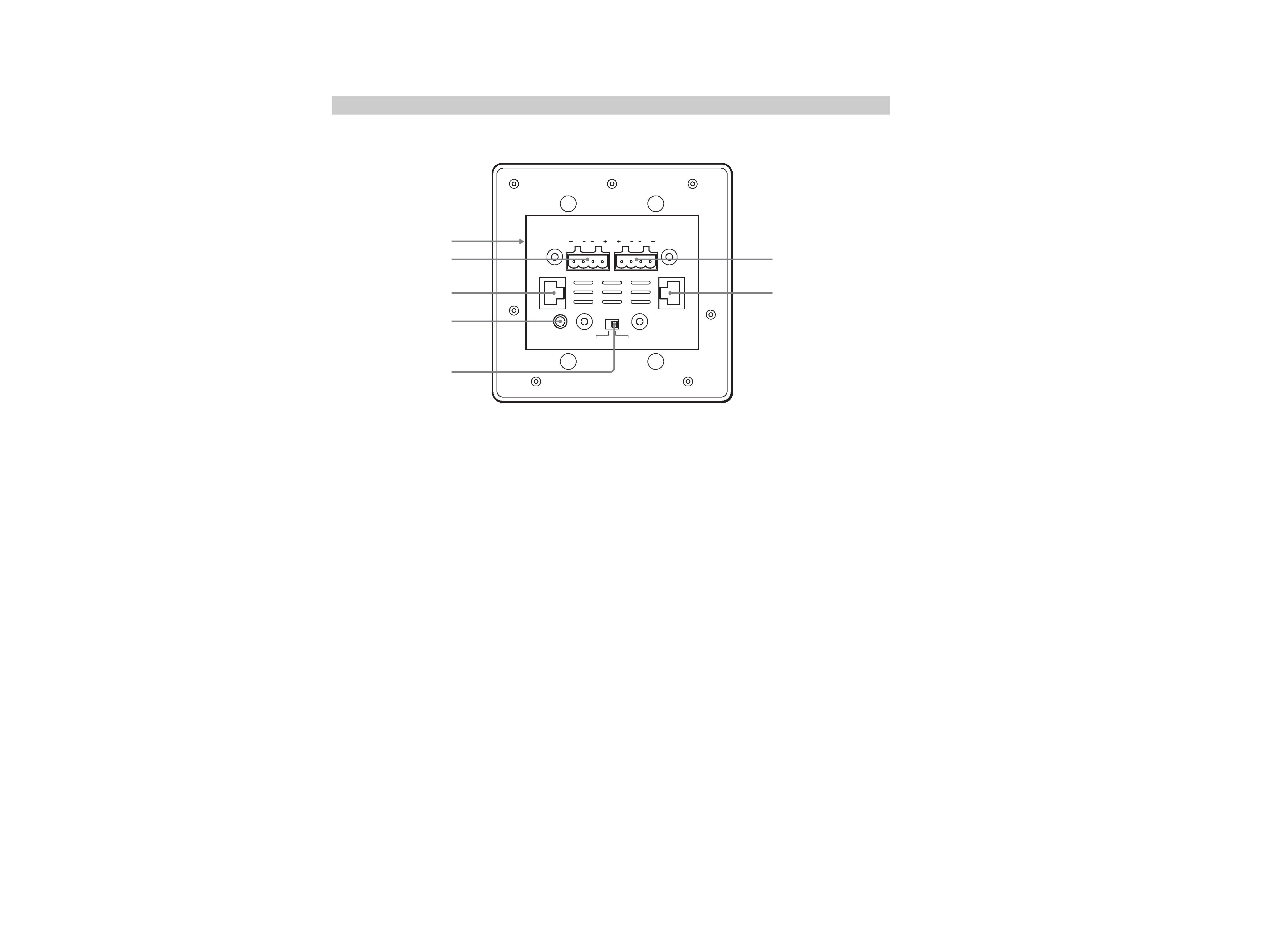
Rear panel of the Keypad
IR IN
OUT
R
TO SPEAKERS
L
DC IN
IN
R
FROM AMPLIFIER
MODE
SUB
L
MAIN
wa
qj
qh
ws
qk
ql
w;
qh
Brightness adjustment hole (page 29)
The hole is located on the side.
Use a flathead screwdriver to adjust the brightness of
the background of the display window.
qj
TO SPEAKERS (page 28)
Connects speaker cords to the speakers in a zone.
qk
OUT (page 28)
Connects a CAT5 straight cable to the IN jack of the
subsidiary Keypad when used in a single room.
ql
IR IN (page 28)
Connects an optional IR emitter so you can operate the
IR Remote Control for the Keypad by pointing it at the
IR sensor of the connected IR emitter.
w;
MODE switch (page 28)
When using two Keypads in a single room, set this
switch to SUB on the subsidiary Keypad.
wa
FROM AMPLIFIER (page 28)
Connect speaker cords to the Main Unit.
ws
IN (page 28)
Connects a CAT5 cable from the Main Unit to the main
Keypad.
5
5
RMR-K100
RMR-K100
SECTION 2
DIAGRAMS
· Circuit Boards Location
Note on Printed Wiring Board:
· Y : parts extracted from the conductor side.
·
: Pattern from the side which enables seeing.
Note on Schematic Diagram:
· All capacitors are in µF unless otherwise noted. (p: pF)
50 WV or less are not indicated except for electrolytics and
tantalums.
· All resistors are in
and 1/4 W or less unless otherwise
specified.
· C : panel designation.
· A : B+ Line.
·Power voltage is dc 12 V and fed with regulated dc power
supply from connector (CN500).
·Voltages and waveforms are dc with respect to ground un-
der no-signal (detuned) conditions.
no mark : Power ON
·Voltages are taken with a VOM (Input impedance 10 M
).
Voltage variations may be noted due to normal production
tolerances.
·Waveforms are taken with a oscilloscope.
Voltage variations may be noted due to normal production
tolerances.
· Circled numbers refer to waveforms.
· Signal path.
F
: AUDIO
Caution:
Pattern face side: Parts on the pattern face side seen from
(Side B)
the pattern face are indicated.
Parts face side:
Parts on the parts face side seen from
(Side A)
the parts face are indicated.
FRONT DISPLAY board
BOTTOM SUPPLY board
SPEAKER board
COMM RIGHT board
COMM LEFT board
·Waveform
1 IC300 is (XO)
62.5ns
3.0Vp-p
1V/DIV, 40ns/DIV
· Indication of transistor.
C
B
These are omitted.
E
Q